

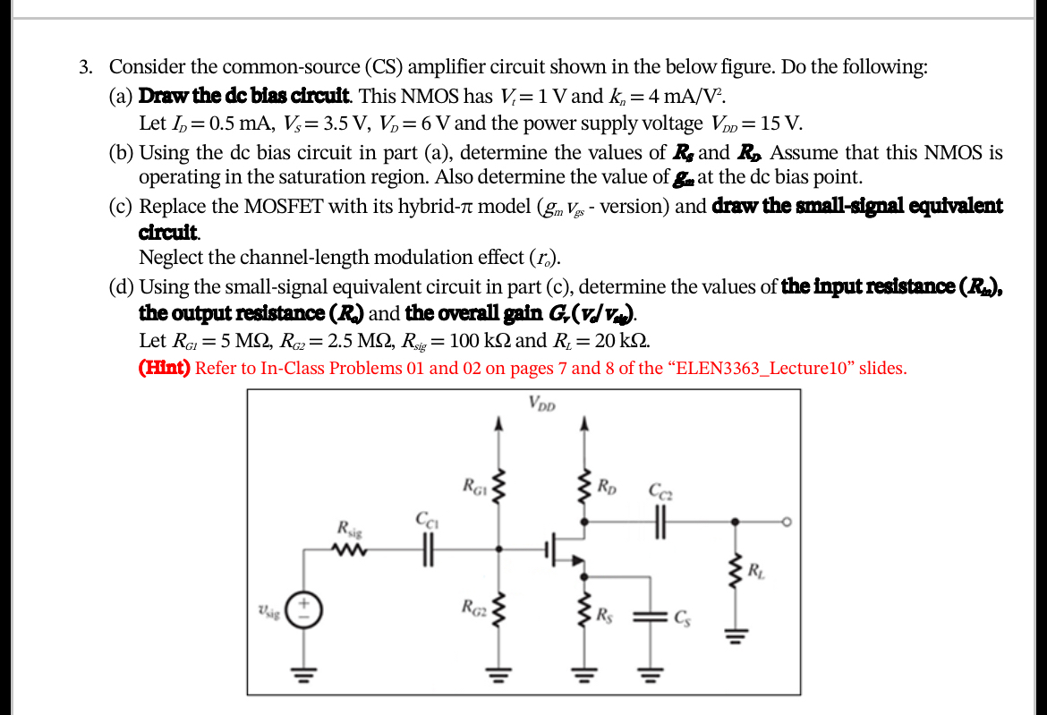
Question: Consider the common - source ( CS ) amplifier circuit shown in the below figure. Do the following: ( a ) Draw the de bias
Consider the commonsource CS amplifier circuit shown in the below figure. Do the following:
a Draw the de bias circuit. This NMOS has and
Let and the power supply voltage
b Using the dc bias circuit in part a determine the values of and Assume that this NMOS is operating in the saturation region. Also determine the value of at the dc bias point.
c Replace the MOSFET with its hybrid model version and draw the smallsignal equivalent circuit.
Neglect the channellength modulation effect
d Using the smallsignal equivalent circuit in part c determine the values of the input resistance the output resistance and the overall gain
Let and
Hint Refer to InClass Problems and on pages and of the "ELENLecture slides.
Step by Step Solution
There are 3 Steps involved in it
1 Expert Approved Answer
Step: 1 Unlock

Question Has Been Solved by an Expert!
Get step-by-step solutions from verified subject matter experts
Step: 2 Unlock
Step: 3 Unlock