Question: Q) Source and drain junction with step function were produced using p-type Si wafer uniformly doped with Na=1 x 1016 cm3 value. At this time,

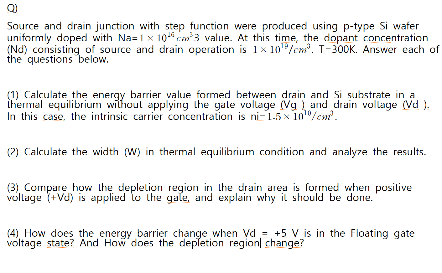
Q) Source and drain junction with step function were produced using p-type Si wafer uniformly doped with Na=1 x 1016 cm3 value. At this time, the dopant concentration (Nd) consisting of source and drain operation is 1 x 10¹⁹/cm. T=300K. Answer each of the questions below. (1) Calculate the energy barrier value formed between drain and i substrate in a thermal equilibrium without applying the gate voltage (Vg) and drain voltage (Vd ). In this case, the intrinsic carrier concentration is ni=1.5 x 10¹⁰/cm'. (2) Calculate the width (W) in thermal equilibrium condition and analyze the results. (3) Compare how the depletion region in the drain area is formed when positive voltage (+Vd) is applied to the gate, and explain why it should be done. (4). How does the energy barrier change when yd = +5 V is in the Floating gate voltage state? And How does the depletion region change? Q) Source and drain junction with step function were produced using p-type Si wafer uniformly doped with Na=1 x 1016 cm3 value. At this time, the dopant concentration (Nd) consisting of source and drain operation is 1 x 10¹⁹/cm. T=300K. Answer each of the questions below. (1) Calculate the energy barrier value formed between drain and i substrate in a thermal equilibrium without applying the gate voltage (Vg) and drain voltage (Vd ). In this case, the intrinsic carrier concentration is ni=1.5 x 10¹⁰/cm'. (2) Calculate the width (W) in thermal equilibrium condition and analyze the results. (3) Compare how the depletion region in the drain area is formed when positive voltage (+Vd) is applied to the gate, and explain why it should be done. (4). How does the energy barrier change when yd = +5 V is in the Floating gate voltage state? And How does the depletion region change
Step by Step Solution
There are 3 Steps involved in it

Get step-by-step solutions from verified subject matter experts


