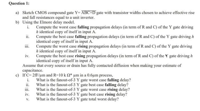
Question: Question 1: a) Sketch CMOS compound gate Y= ABC+D gate with transistor widths chosen to achieve effective rise and fall resistances equal to a unit

Question 1: a) Sketch CMOS compound gate Y= ABC+D gate with transistor widths chosen to achieve effective rise and fall resistances equal to a unit inverter. b) Using the Elmore delay model. i Compute the worst case falling propagation delays (in term of Rand C) of the Y gate driving h identical copy of itself in input A. ii. Compute the best case falling propagation delays (in term of Rand C) of the Y gate driving h identical copy of itself in input A. iii. Compute the worst case rising propagation delays (in term of Rand C) of the Y gate driving h identical copy of itself in input A. iv. Compute the best case rising propagation delays (in term of Rand C) of the Y gate driving h identical copy of itself in input A. Assume that every source or drain has fully contacted diffusion when making your estimate of capacitance. c) IfC=2fF/um and R=10k * um in a 0.6um process, i. What is the fanout-of-3 Y gate worst case falling delay? ii. What is the fanout-of-3 Y gate best case falling delay? What is the fanout-of-3 Y gate worst case rising delay? iv. What is the fanout-of-3 Y gate best case rising delay? What is the fanout-of-3 Y gate total worst delay? 111. V
Step by Step Solution
There are 3 Steps involved in it

Get step-by-step solutions from verified subject matter experts


