

Question: Question 2. Consider the data path shown in Figure 4.2. Assume that the components have the following latencies in picoseconds (ps). Component Mux (each) ALU
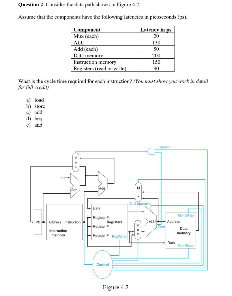
Question 2. Consider the data path shown in Figure 4.2. Assume that the components have the following latencies in picoseconds (ps). Component Mux (each) ALU Add (each) Data memory Instruction memory Registers (read or write) Latency in ps 20 130 50 200 150 90 What is the cycle time required for each instruction? (You must show you work in detail for full credit) a) load b) store c) add d) beq e) and Branch 4 Add Add M u ALU operation Data PC Address Instruction Register # Registers Register # M Mem Write > ALU Address Zero Data memory Instruction memory Register # RegWrite Data MemRead Control Figure 4.2
Step by Step Solution
There are 3 Steps involved in it
1 Expert Approved Answer
Step: 1 Unlock

Question Has Been Solved by an Expert!
Get step-by-step solutions from verified subject matter experts
Step: 2 Unlock
Step: 3 Unlock