

Question: computer archietcture please show steps Assume that the single-instruction/cycle datapath shown below Add 4 Add Sum Shift left 1 Branch MemRead MemtoRe Instruction [6-0] Control
computer archietcture please show steps
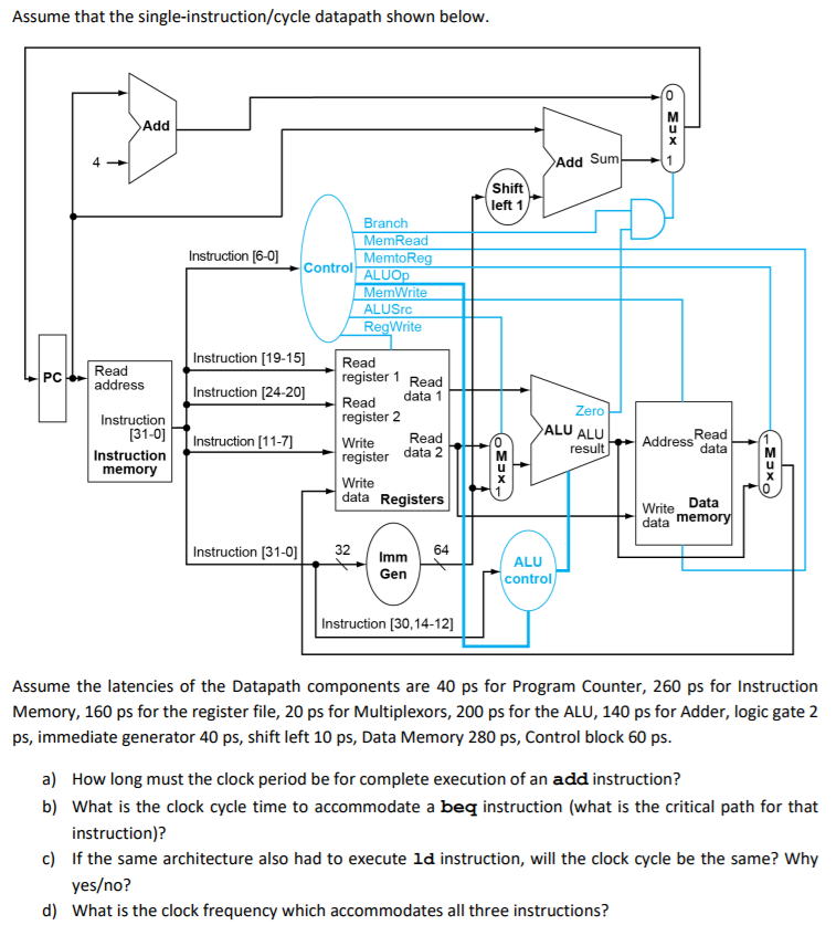
Assume that the single-instruction/cycle datapath shown below Add 4 Add Sum Shift left 1 Branch MemRead MemtoRe Instruction [6-0] Control ALU ALUSro RegWrite Instruction [19-15]Read Read register 1 Read Read data 1 register 2 Write register data 2 Write data Registers PCaddress Instruction [24-20] Instruction [31-0nstruction [11-7] ALU ALU Read resultAddressRead Instruction memory Write Data data me Instruction [31-0]| 32, Imm 64 Gen ALU control Instruction [30,14-12] Assume the latencies of the Datapath components are 40 ps for Program Counter, 260 ps for Instruction Memory, 160 ps for the register file, 20 ps for Multiplexors, 200 ps for the ALU, 140 ps for Adder, logic gate 2 ps, immediate generator 40 ps, shift left 10 ps, Data Memory 280 ps, Control block 60 ps a) How long must the clock period be for complete execution of an add instruction? b) What is the clock cycle time to accommodate a beq instruction (what is the critical path for that c) d) instruction)? If the same architecture also had to execute ld instruction, will the clock cycle be the same? Why yeso? What is the clock frequency which accommodates all three instructions? Assume that the single-instruction/cycle datapath shown below Add 4 Add Sum Shift left 1 Branch MemRead MemtoRe Instruction [6-0] Control ALU ALUSro RegWrite Instruction [19-15]Read Read register 1 Read Read data 1 register 2 Write register data 2 Write data Registers PCaddress Instruction [24-20] Instruction [31-0nstruction [11-7] ALU ALU Read resultAddressRead Instruction memory Write Data data me Instruction [31-0]| 32, Imm 64 Gen ALU control Instruction [30,14-12] Assume the latencies of the Datapath components are 40 ps for Program Counter, 260 ps for Instruction Memory, 160 ps for the register file, 20 ps for Multiplexors, 200 ps for the ALU, 140 ps for Adder, logic gate 2 ps, immediate generator 40 ps, shift left 10 ps, Data Memory 280 ps, Control block 60 ps a) How long must the clock period be for complete execution of an add instruction? b) What is the clock cycle time to accommodate a beq instruction (what is the critical path for that c) d) instruction)? If the same architecture also had to execute ld instruction, will the clock cycle be the same? Why yeso? What is the clock frequency which accommodates all three instructions
Step by Step Solution
There are 3 Steps involved in it

Get step-by-step solutions from verified subject matter experts