

Question: Using the software WinLogiLab to design a simple parity generator/checker circuit PRE-LAB Pre-lab work must be completed individually prior to the lab session. The pre-lab
Using the software WinLogiLab to design a simple parity generator/checker circuit
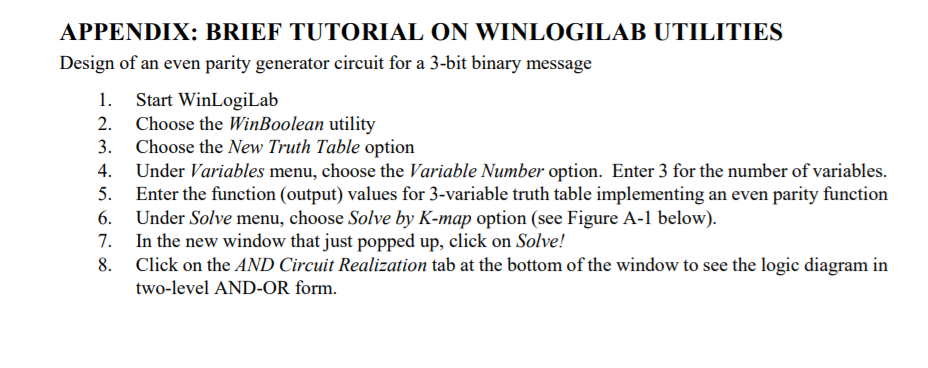
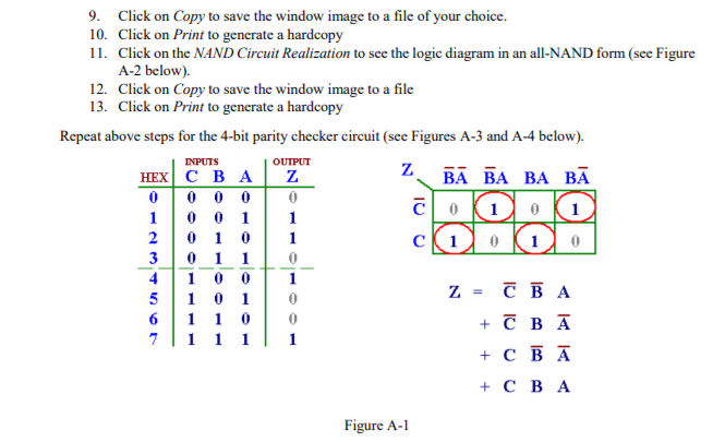
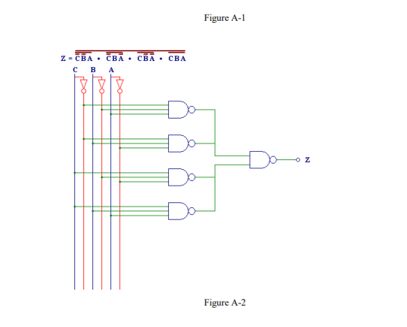
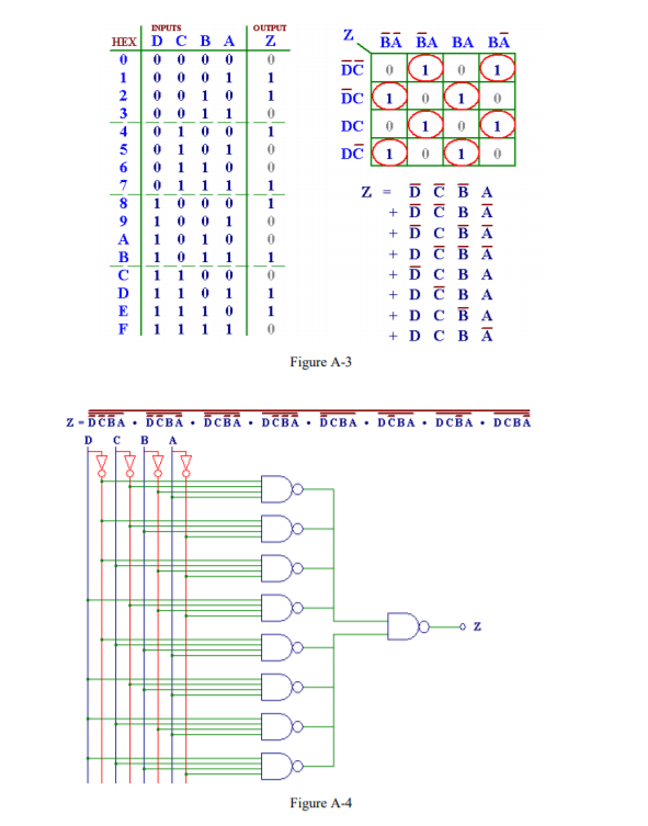
PRE-LAB Pre-lab work must be completed individually prior to the lab session. The pre-lab for this lab assignment will constitute 40% of your lab grade. You must deliver a hard copy documenting your individually per formed pre-lab work to your lab instructor at the start of your scheduled lab session Task 1 Go through the tutorial on using WinLogiLab to design a simple parity generator/checker circuit in the Appendix. Implement each step and make sure you obtain the same outputs from WinLogiLab. Task 2 Manually generate the truth table for even parity function (P) for a 2-bit message (x, y). Manually derive the algebraic expression for the Boolean function P. Manually minimize the Boolean function for P (i.e. use either a Karnaugh map or Boolean algebra) and generate the minimal AND-OR realization. Task 3 Use WinLogiLab to derive both the minimal AND-OR and the equivalent minimal all-NAND gate realiza- tions for P (see Figures A-1 and A-2 in the Appendix for a solved example that uses 3 message bits instead of 2). Capture both the AND-OR and all-NAND logical schematics into a file and hard copy. (As a side note, when it comes to physical construction or realization of the logic circuit, it is much easier to locate multi-input NAND gate ICs than multi-input AND gate ICs due to manufacturability of the former.) PRE-LAB Pre-lab work must be completed individually prior to the lab session. The pre-lab for this lab assignment will constitute 40% of your lab grade. You must deliver a hard copy documenting your individually per formed pre-lab work to your lab instructor at the start of your scheduled lab session Task 1 Go through the tutorial on using WinLogiLab to design a simple parity generator/checker circuit in the Appendix. Implement each step and make sure you obtain the same outputs from WinLogiLab. Task 2 Manually generate the truth table for even parity function (P) for a 2-bit message (x, y). Manually derive the algebraic expression for the Boolean function P. Manually minimize the Boolean function for P (i.e. use either a Karnaugh map or Boolean algebra) and generate the minimal AND-OR realization. Task 3 Use WinLogiLab to derive both the minimal AND-OR and the equivalent minimal all-NAND gate realiza- tions for P (see Figures A-1 and A-2 in the Appendix for a solved example that uses 3 message bits instead of 2). Capture both the AND-OR and all-NAND logical schematics into a file and hard copy. (As a side note, when it comes to physical construction or realization of the logic circuit, it is much easier to locate multi-input NAND gate ICs than multi-input AND gate ICs due to manufacturability of the former.)
Step by Step Solution
There are 3 Steps involved in it

Get step-by-step solutions from verified subject matter experts