

Question: A digital clock has become corrupted by a ringing (undesired oscillations) as shown in Figure P7-69. (a). The unwanted oscillations can cause false triggers and
A digital clock has become corrupted by a ringing (undesired oscillations) as shown in Figure P7-69. (a). The unwanted oscillations can cause false triggers and must be reduced to not trigger a false logic 1 or 0 . The comparators should only trigger when the clock signal is above \(3.7 \mathrm{~V}\) for a logic 1 and below \(1.2 \mathrm{~V}\) for a logic zero. The clocks ringing can be modeled as an \(R L C\) series circuit as shown in Figure P7-69. (b), with the voltage taken at node A. The parasitic capacitance is estimated at 0.01 \(\mu \mathrm{F}\) and the Thévenin resistance at \(220 \Omega\). From the graph, the inductance is estimated at \(15 \mathrm{mH}\). Build the circuit as shown in Figure P7-69. (b). Do a transient analysis and observe how the ringing causes false logic outputs. Now design an interface circuit that significantly reduces the ringing without significantly reducing the rise time (the time it takes the pulse to go from low to high or vice versa). The transition must occur in less than 80 us and the overshoot and undershoot (deviation from 0 or \(5 \mathrm{~V}\) ) must not cause unwanted triggering. A logic " 1 " must always be greater than \(3.7 \mathrm{~V}\) and a logic "o" must always be less than 1.2 V. Use Multisim to validate your design. The comparator outputs should always be either a logic 1 or a logic 0 .
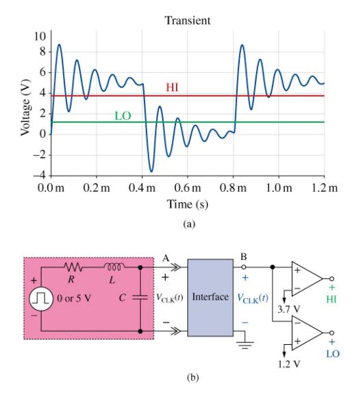
Voltage (V) 10 8 9 42 -2 -4 0.0 m HI Am my Wome LO 0.2 m www R 0 or 5 V 000 L C Transient 0.4 m 0.6 m 0.8 m 1.0m 1.2m Time (s) (a) B + VCLK() Interface VCLK(1) (b) + 3.7 V 1.2 V + HI + LO
Step by Step Solution
3.48 Rating (158 Votes )
There are 3 Steps involved in it

Get step-by-step solutions from verified subject matter experts