New Semester
Started
Get
50% OFF
Study Help!
--h --m --s
Claim Now
Question Answers
Textbooks
Find textbooks, questions and answers
Oops, something went wrong!
Change your search query and then try again
S
Books
FREE
Study Help
Expert Questions
Accounting
General Management
Mathematics
Finance
Organizational Behaviour
Law
Physics
Operating System
Management Leadership
Sociology
Programming
Marketing
Database
Computer Network
Economics
Textbooks Solutions
Accounting
Managerial Accounting
Management Leadership
Cost Accounting
Statistics
Business Law
Corporate Finance
Finance
Economics
Auditing
Tutors
Online Tutors
Find a Tutor
Hire a Tutor
Become a Tutor
AI Tutor
AI Study Planner
NEW
Sell Books
Search
Search
Sign In
Register
study help
business
systems analysis and design
The Analysis And Design Of Linear Circuits 8th Edition Roland E. Thomas, Albert J. Rosa, Gregory J. Toussaint - Solutions
Construct a Butterworth low-pass transfer function that meets the following requirements:TMAX = 0 dB,TMIN = −40 dB, ωC = 250 rad=s, and ωMIN =1:5 krad=s.
The circuit design in Example 14–7 used the equal element method. Rework the problem using the unity gain technique. Use Multisim to validate your design. Comment on the two approaches.
(a) Construct a Butterworth low-pass transfer function that meets the following requirements:TMAX = 20 dB,ωC = 1 krad=s,TMIN = −20 dB, and ωMIN = 4 krad=s:(b) Design a cascade of active RC circuits that realizes the transfer function found in part (a). Validate your design using Multisim
Construct a first-order cascade transfer function that meets the following requirements:TMAX = 0 dB,TMIN = −30 dB,ωC = 200 rad=s, and ωMIN = 1 krad=s.
(a) Construct a first-order cascade transfer function that meets the following requirements:TMAX = 10 dB,ωC = 200 rad=s,TMIN = −10 dB, and ωMIN = 800 rad=s.Use MATLAB to visualize the gain plot.(b) Design a cascade of active RC circuits that realizes the transfer function developed in (a). Use
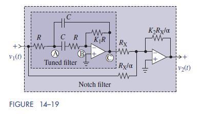
Design a notch filter using the realization in Figure 14–19 to achieve a notch at 200 krad=s, a B of 20 krad=s, and a passband gain of 10. C w R CR KR KRxl ww ww Rx (B www V(f) + Tuned filter Rxla V2(f) ww Notch filter FIGURE 14-19
Use the active RC circuit in Figure 14–19 to design a bandstop filter with a notch frequency at 60 Hz and a notch bandwidth of 12 Hz. Find the circuit’s transfer function and use Multisim to plot the filter’s gain characteristic and to estimate the attenuation of the notch. Compare your
Construct a second-order bandstop transfer function with a notch frequency of 50 rad=s, a notch bandwidth of 10 rad=s, and passband gains of 5
Rework the circuit design in Example 14–4 starting with C1 =C2 =C =0:2 μF.
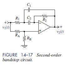
Use the active RC circuit in Figure 14–17 to design a bandstop filter with a notch frequency at 60 Hz and a notch bandwidth of 12 Hz. Find the circuit’s transfer function and use MATLAB to plot the filter’s gain characteristic and to estimate the attenuation of the notch. Then use Multisim to
Construct a second-order bandpass transfer function with a corner frequency of 50 rad=s, a bandwidth of 10 rad=s, and a center frequency gain of 4.
Rework the design in Example 14–3, starting with C = 2000 pF.
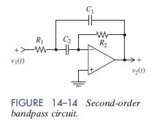
Use the active RC circuit in Figure 14–14 to design a bandpass filter with a center frequency at 10 kHz and a bandwidth of 4 kHz. Find the center frequency gain for the design. Use MATLAB to show the filter’s gain characteristics R +W- v(1) C ww C R 12(1) FIGURE 14-14 Second-order bandpass
Construct a second-order high-pass transfer function with a corner frequency of 20 rad=s, an infinite-frequency gain of 4, and a gain of 2 at the corner frequency.
Develop a second-order high-pass transfer function with a corner frequency atω0 = 20 krad=s, an infinite-frequency gain of 0 dB, and a corner frequency gain of−3 dB. Use MATLAB to help visualize the Bode magnitude plot of the desired transfer function. Then design two competing circuits using
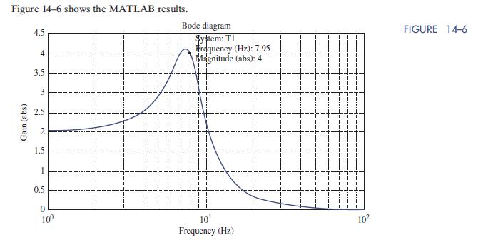
Design circuits using both the equal element design and unity gain design techniques to realize the transfer function in Exercise 14–1. Use Multisim to simulate your designs and compare them to the MATLAB results shown in Figure 14–6. Gain (abs) 3. Figure 14-6 shows the MATLAB results. 4.5 4
Develop a second-order low-pass transfer function with a corner frequency of 50 rad=s or 7:96 Hz, a dc gain of 2, and a gain of 4 at the corner frequency. Validate your result by using MATLAB to plot the transfer function’s absolute gain versus frequency
Develop a second-order low-pass transfer function with a corner frequency atω0 = 1 krad=s and with corner frequency gain equal to the dc gain. Use MATLAB to help visualize the Bode plots of the desired transfer function. Then design two competing circuits using the equal element and unity gain
14-4 High-Pass, Bandpass, and Bandstop Filter Design(Sects. 14–6 and 14–7)Given a high-pass, bandpass, or bandstop filter specification:(a) Construct a transfer function that meets the specification.(b) Design a cascade or parallel connection of first- and second-order circuits that implements
14-3 Low-Pass Filter Design (Sects. 14–4 and 14–5)Given a low-pass filter specification:(a) Construct a transfer function that meets the specification.(b) Design a cascade of first- and second-order circuits that implements a given transfer function.(c) Select the best design from competitive
14-2 Second-Order Filter Design (Sects. 14–2 and 14–3)(a) Construct a second-order transfer function with specified filter characteristics.(b) Design a second-order circuit with specified filter characteristics.
14-1 Second-Order Filter Analysis (Sects. 14–1, 14–2 and 14–3)(a) Given a second-order filter circuit, find a specified transfer function.(b) Given the transfer function of a second-order circuit, develop a method of selecting the element values to achieve specified filter characteristics.
13–56 Virtual Keyboard Design Electronic keyboards are designed using the following equation that assigns particular frequencies to each of the 88 keys in a standard piano keyboard:where n is the key number. There is a need for an amplifier that can pass high C, key 64, but block keys 63 and 65.
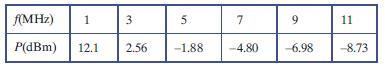
13–55 Spectrum Analyzer Calibration A certain spectrum analyzer measures the average power delivered to a calibrated resistor by the individual harmonics of periodic waveforms. The calibration of the analyzer has been checked by applying a 1-MHz square wave and the following results reported:The
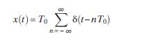
13–53 Spectrum of a Periodic Impulse Train A periodic impulse train can be written asFind the Fourier coefficients of x(t). Plot the amplitude spectrum and comment on the frequencies contained in the impulse train. x(t) To (t-nTo) 12--00
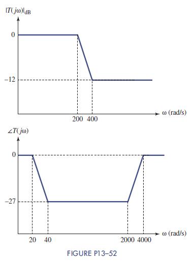
13–52 Fourier Series from a Bode Plot The transfer function of a linear circuit has the straightline gain and phase Bode plots in Figure P13–52. The first four terms in the Fourier series of a periodic input v1(t) to the circuit areEstimate the amplitudes and phase angles of the first four
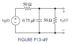
13–49 The input to the circuit in Figure P13–49 is the voltage(a) Calculate the average power delivered to the 50-Ω load resistor.(b) Use Multisim to find the magnitude of the voltage across the load resistor for each of the two inputs. Then apply Eq (13–24) to find Vrms and Eq (13–25) to
13–48 Estimate the rms value of the periodic voltage 1 v(t) =VA [2-cos(opt) + cos(3 opt) - cos(5 mot) 1 +cos(7 opt)
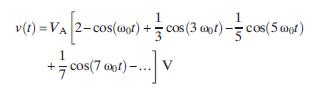
13–45 Repeat Problem 13–44 for the periodic waveform in Figure P13–45. Vs(f) (V) VA t(s) 0 2T FIGURE P13-45
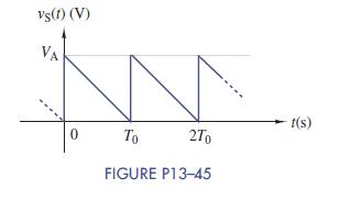
13–44 Find the rms value of the periodic waveform in Figure P13–44 and the average power the waveform delivers to a resistor. Find the dc component of the waveform and the average power carried by the dc component. What fraction of the total average power is carried by the dc component?What
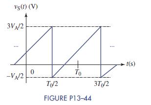
13–38 The voltage across a 100-Ω resistor is given by the an Fourier coefficients shown in volts in Figure P13–38. All bn coefficients are zero, as is a0. The fundamental frequency is 250 Hz.(a) Find expressions for the current through the resistor and the power dissipated by the resistor.(b)
13–37 The current through a 1-kΩ resistor isFind the rms value of the current and the average power delivered to the resistor. i(t)=50+36cos(120-30)-12 cos(360+45) mA
13–36 A triangular wave with VA = 10 V and T0 =20π ms drives a circuit whose transfer function is(a) Find the amplitude of the first four nonzero terms in the Fourier series of the steady-state output. What term in the Fourier series tends to dominate the response? Explain.(b) Repeat Part (a)
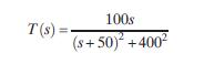
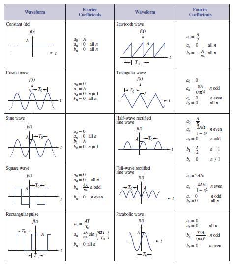
13–29 The periodic triangular wave in Figure P13–29 is applied to the RLC circuit shown in the figure.(a) Use the results in Figure 13–4 to find the Fourier coefficients of the input for VA = 5 V and T0 = 400π μs.(b) Find the amplitude of the first five nonzero terms in the Fourier series
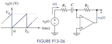
13–26 The periodic sawtooth wave in Figure P13–26 drives the OP AMP circuit shown in the figure.(a) Use the results in Figure 13–4 to find the Fourier coefficients of the input for VA = 3 V and T0 =4π ms.(b) Find the first four nonzero terms in the Fourier series of vO(t) for R1 =20 kΩ, R2
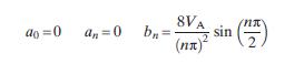
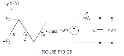
13–25 The periodic triangular wave in Figure P13–25 is applied to the RC circuit shown in the figure. The Fourier coefficients of the input areIf VA = 10 V and T0 =2π ms, find the first four nonzero terms in the Fourier series of vO(t) for R=5 kΩ and C =0:01 μF. 0=" 0=0p 8VA bm=- (nx) sin (
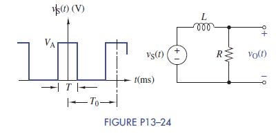
13–24 The periodic pulse train in Figure P13–24 is applied to the RL circuit shown in the figure.(a) Use the results in Figure 13–4 to find the Fourier coefficients of the input for VA =12V, T0 = π ms, and T =T0=4.(b) Find the first four nonzero terms in the Fourier series of vO(t) for R=
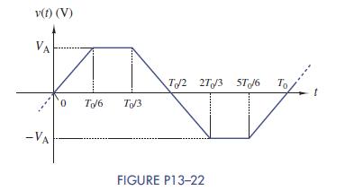
13–22 Find the Fourier series for the waveform in Figure P13–22. v(t) (V) VA T/2 2T/3 ST/6 ST/6 To 0 To/6 To/3 -VA FIGURE P13-22
13–20 The first five terms in the Fourier series of a periodic waveform are(a) Find the period and fundamental frequency in rad/s and Hz. Identify the harmonics present in the first five terms.(b) Use MATLAB to plot two periods of v(t).(c) Identify the symmetry features of the waveform.(d) Write
13–19 The first four terms in the Fourier series of a periodic waveform are(a) Find the period and fundamental frequency in rad/s and Hz. Identify the harmonics present in the first four terms.(b) Identify the symmetry features of the waveform.(c) Write the first four terms in the Fourier series
13–18 The equation for a periodic waveform is(a) Sketch the first two cycles of the waveform and identify a related signal in Figure 13–4.(b) Use the Fourier series of the related signal to find the Fourier coefficients of v(t).(c) Use MATLAB to sketch an estimate for the signal using the
13–17 The equation for the first cycle (0 ≤ t ≤ T0) of a periodic pulse train is(a) Sketch the first two cycles of the waveform and identify a related signal in Figure 13–4.(b) Use the Fourier series of the related signal to find the Fourier coefficients of v(t). v(t)=VAu(31-To)-u(31-2T0)]V
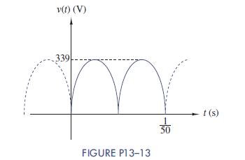
13–13 Use the results in Figure 13–4 to calculate the Fourier coefficients of the full-wave rectified sine wave in Figure P13–13.Use MATLAB to verify your results. Write an expression for the first four nonzero terms in the Fourier series. v(t) (V) 339 FIGURE P13-13 50 t(s)
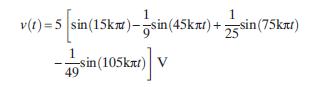
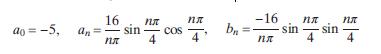
13–12 A particular periodic waveform with a period of 10 ms has the following Fourier coefficients(a) Write an expression for the terms in the Fourier series up to n=8.(b) Convert your expression in to amplitude and phase form and plot its spectrum. a0=-5, 16 sin an= COS 4 bn -16 sin 4 sin
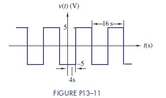
13–11 Derive expressions for the Fourier coefficients of the periodic waveform in Figure P13–11.(a) Write an expression for the first four nonzero terms in the Fourier series.(b) Plot the spectrum of the Fourier coefficients an and bn. v(t) (V) -16 s- 5 4s FIGURE P13-11 t(s)
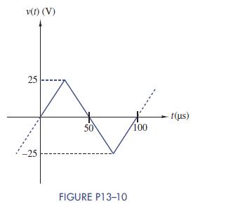
13–10 Use the results in Figure 13–4 to calculate the Fourier coefficients of the shifted triangular wave in Figure P13–10.Write an expression for the first four nonzero terms in the Fourier series. v(f) (V) 25 t(us) 50 100 -25 FIGURE P13-10
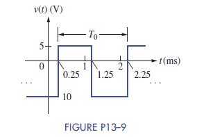
13–9 Find the first five nonzero Fourier coefficients of the shifted and offset square wave in Figure P13–9. Use your results to write an expression in the corresponding Fourier series. v(t) (V) - To 5- 0 t(ms) 2 0.25 1.25 2.25 10 FIGURE P13-9
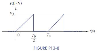
13–8 Derive expressions for the Fourier coefficients of the periodic waveform in Figure P13–8. v(t) (V) VA 0 To 22 To -t(s) FIGURE P13-8
13–6 The equation for the first cycle (0 ≤ t ≤ T0) of a periodic pulse train is(a) Sketch the first two cycles of the waveform.(b) Derive expressions for the Fourier coefficients an and bn.13–7 The equation for the first cycle (0 ≤ t ≤ T0) of a periodic waveform is(a) Sketch the first
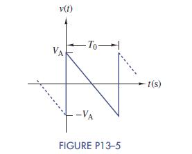
13–5 Derive expressions for the Fourier coefficients of the periodic waveform in Figure P13–5. v(t) VA -To- -VA FIGURE P13-5 -t(s)
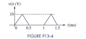
13–4 Derive expressions for the Fourier coefficients of the periodic waveform in Figure P13–4. v(f) (V) 10 t(ms) '0 0.5 1 1.5 FIGURE P13-4
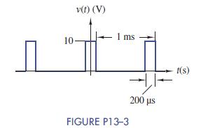
13–3 Derive expressions for the Fourier coefficients of the periodic waveform in Figure P13–3. v(t) (V) 1 ms 10- I(s) FIGURE P13-3 200 s
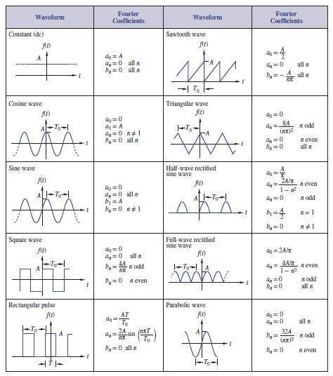
In the rectangular-pulse waveform shown in Figure 13–4, the width of the pulse is one-third the period, T =T0=3. The waveform is to pass through a low-pass filter and then through a resistive load. The load must receive at least 97% of the average power in the original waveform.Determine the
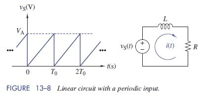
Figure 13–8 shows a series RL circuit driven by a sawtooth voltage source. Estimate the average power delivered to the resistor for VA =25V, R= 50, Ω, L=40 μH, T0 =5 μs, and ω0 =2π=T0 =1:26 Mrad=s. Vs(V) VA Vs(f) t(s) 0 To 2T (+1 L i(t) R FIGURE 13-8 Linear circuit with a periodic input.
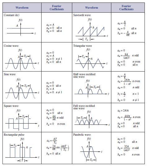
The full–wave rectified sine wave shown in Figure 13–4 has an rms value of A=ffiffiffi p2. What fraction of the average power that the waveform delivers to a resistor is carried by the first two nonzero terms in its Fourier series? Waveform Constant (dc) A Cosine wave fit) Fourier Coefficients
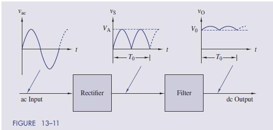
Figure 13–11 shows a block diagram of a dc power supply. The ac input is a sinusoid that is converted in to a full-wave sine by the rectifier. The filter passes the dc component in the rectified sine and suppresses the ac components. The result is an output consisting of a small residual ac
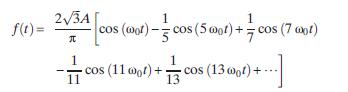
(a) Identify the symmetries in the waveform f t ð Þ whose Fourier series is(b) Write the corresponding terms of the function gðtÞ = f ðt−T0=4Þ. f(t)= 23A 11 1 cos (wot)-cos (5 wot) + cos (7 cot) cos (11 of) + cos (13 pt) +
Given that f ðtÞ is a square wave of amplitude A and period T0, use the Fourier coefficients in Figure 13–4 to find the Fourier coefficients of gðtÞ = f ðt + T0=4Þ. Waveform Constant (dc) A Fourier Coefficients a=0 all n b=0 all Cosine wave fit) -To- AM Sine wave f(r) AL-To- AM Square wave
Derive expressions for the amplitude An and phase angle ϕn for the triangular wave in Figure 13–4 and write an expression for the first three nonzero terms in the Fourier series with A= π2=8 and T0 =2π=5000 s. Waveform Constant (dc) A Fourier Coefficients a=0 all n b=0 all Cosine wave fit)
Derive expressions for the amplitude An and phase angle ϕn of the Fourier series of the sawtooth wave in Figure 13–4. Sketch the amplitude and phase spectra of a sawtooth wave with A= 5 and T0 = 4 ms Waveform Constant (dc) A Fourier Coefficients a=0 all n b=0 all Cosine wave fit) -To- AM Sine
The triangular wave in Figure 13–4 has a peak amplitude of A= 10 and T0 = 2 ms. Calculate the Fourier coefficients of the first nine harmonics. Waveform Constant (dc) A Cosine wave fit) Fourier Coefficients a=0 all n b=0 all -To- AM Sine wave fin) AL-To- AM Square wave K(1) ag=0 a = A 4 01 b=0
Verify the Fourier coefficients given for the square wave in Figure 13–4 and write the first three nonzero terms in its Fourier series. Waveform Constant (dc) A Cosine wave fit) Fourier Coefficients a=0 all n b=0 all Waveform Fourier Coefficients Sawtooth wave fir) %=0 all s b=- To Triangular
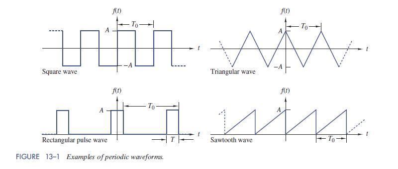
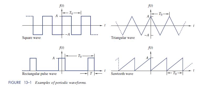
Given a rectangular pulse waveform as shown in Figure 13–1, letA= 10,T0 = 5 ms,and T = 2 ms. (a) UseMATLABto calculate the Fourier coefficients for the first 10 harmonics. (b) Use the 10 harmonics to plot a truncated series representation of the waveform. f(t) To- A Square wave f(t) A To
Find the Fourier coefficients for the rectangular pulse wave in Figure 13–1. f(t) To- A f(t) To- Square wave A f(t) To Triangular wave f(t) ninaiva Rectangular pulse wave FIGURE 13-1 Examples of periodic waveforms. Sawtooth wave 14
Find the Fourier coefficients for the sawtooth wave in Figure 13–1. Square wave A A f(t) f(t) To- To Triangular wave A f(t) f(t) To- ninaia Rectangular pulse wave FIGURE 13-1 Examples of periodic waveforms. Sawtooth wave A t
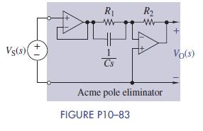
10–83 Pole Eliminator Circuit The Acme Pole Eliminator Company states in their online catalog that the circuit shown in Figure P10–83 can eliminate any realizable pole. Their catalog states “Suppose you have a need to eliminate the pole associated with an input, for example, VSðsÞ = K=ðs +
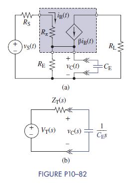
10–82 By-Pass Capacitor Design In transistor amplifier design, a by-pass capacitor is connected across the emitter resistorRE to effectively short out the emitter resistor at signal frequencies. This design improves the gain of the transistor for the desired ac signals. The circuit in Figure
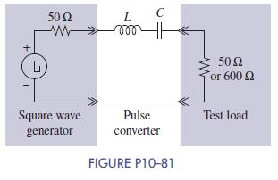
10–81 Pulse Conversion Circuit The purpose of the test setup in Figure P10–81 is to deliver damped sine pulses to the test load. The excitation comes from a 1-Hz square wave generator. The pulse conversion circuit must deliver damped sine waveforms with ζ ω0 > 10 krad=s to 50-Ω and 600-Ω
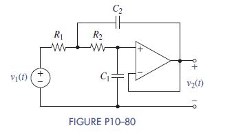
10–80 s-domain OP AMP Circuit Analysis The OP AMP circuit in Figure P10–80 is in the zero state.Transform the circuit into the s domain and use the OP AMP circuit analysis techniques developed in Section 4-4 to find the relationship between the input V1ðsÞ and the output V2ðsÞ. V(t) C R R
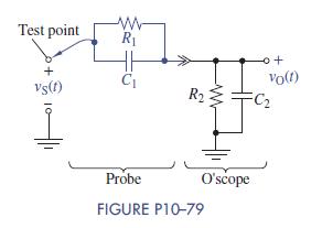
10–79 RC Circuit Analysis and Design The RC circuits in Figure P10–79 represent the situation at the input to an oscilloscope. The parallel combination of R1 and C1 represents the probe used to connect the oscilloscope to a test point. The parallel combination of R2 and C2 represents the input
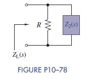
10–78 Design a Load Impedance In order to match the Thévenin impedance of a source, the load impedance in Figure P10–78 must(a) What impedance Z2ðsÞ is required if R = 20 Ω?(b) How would you realize Z2ðsÞ using only resistors, inductors, and/or capacitors? (Hint:Write ZLðsÞ as a sum of
10–77 Thévenin’s Theorem from Time-Domain Data A black box containing a linear circuit has an on-off switch and a pair of external terminals. When the switch is turned on, the open-circuit voltage between the external terminals is observed to beThe short-circuit current was observed to
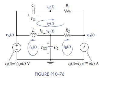
10–76 The circuit in Figure P10–76 is shown in the t domain with initial values for the energy storage devices.(a) Transform the circuit into the s domain and write a set of node-voltage equations.(b) Transform the circuit into the s domain and write a set of mesh-current equations.(c) With the
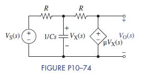
10–74 Find the range of the gain μ for which the circuit’s output VOðsÞ in Figure P10–74 is stable (i.e., all poles are in the lefthand side of the s plane.) Vs(s) +1 R R www w 1/Cs Vx(s) Vo(s) HVx(s) FIGURE P10-74
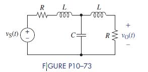
10–73 Show that the circuit in Figure P10–73 has natural poles at s = −4=RC and s = −2=RC ± j2=RC when L = R2C=4: vs(t) R L FIGURE P10-73 L 000 + R vo(t)
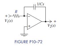
10–72 With the circuit in the zero state, the input to the integrator shown in Figure P10–72 is v1ðtÞ = cos 2000 t V. The desired output is v2ðtÞ = −sin 2000 t V. Use Laplace to select values ofR and C to produce the desired output. If the capacitor had 5 V across it at t = 0, how would
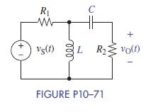
10–71 There is no initial energy stored in the circuit in Figure P10–71.(a) Transform the circuit into the s domain.(b) Then use the unit output method to find the ratio VOðsÞ=VSðsÞ.(c) If vSðtÞ = δðtÞ and R1 = R2 = 500 Ω, select values of L and C to produce a VOðsÞ with ζ = 0:707
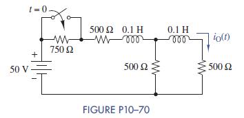
10–70 The switch in Figure P10–70 has been open for a long time and is closed at t = 0. Transform the circuit into the s domain and solve for IOðsÞ and iOðtÞ. 1=0 50 V 500 0.1 0.1 H www 750 + 500 www -000 500 io(t) FIGURE P10-70
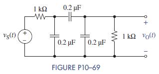
10–69 There is no energy stored in the circuit in Figure P10–69 at t = 0: Transform the circuit into the s domain. Then use the unit output method to find the ratio VOðsÞ=VSðsÞ. Subsequently, use the input vSðtÞ = 100 uðtÞ and find the output vOðtÞ. vs(t) +1 1 w 0.2 F 0.2 F 0.2 F
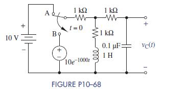
10–68 The switch in Figure P10–68 has been in positionAfor a long time and is moved to position B at t = 0:(a) Write an appropriate set of node-voltage or meshcurrent equations in the s domain.(b) Use MATLAB to solve for VCðsÞ and vCðtÞ. Also using MATLAB, plot vCðtÞ and the exponential
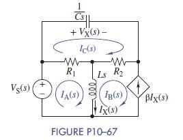
10–67 Three mesh currents are shown in Figure P10–67.(a) Explain why only two of these mesh currents are independent.(b) Write s-domain mesh-current equations in the two independent mesh currents.(c) Find IXðsÞ and VXðsÞ in terms of the mesh currents. Vs($) + I Cs + Vx(s) - w Ic(s) ww R Ls
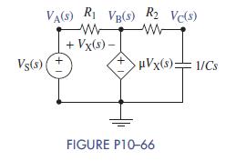
10–66 Three node voltages are shown in Figure P10–66.(a) Explain why only one of the node voltages is independent.(b) Write a node voltage equation in the independent node voltage.(c) If VCðsÞ is the circuit’s output, find the output–input ratio or network function, VCðsÞ=VSðsÞ. VA(S)
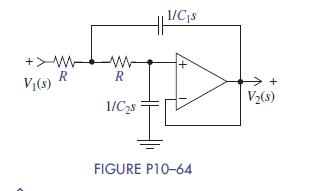
10–64 The OP AMPcircuit in Figure P10–64 is in the zero state. Use node-voltage equations to find the circuit determinant.Select values of R, C1, and C2 so that the circuit hasω0 = 20 krad=s and ζ = 1:0. (Hint: See Example 10–15.) W
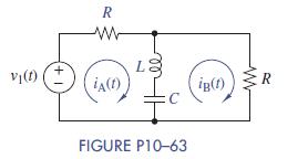
10–63 The circuit in Figure P10–63 is in the zero state.Use mesh-current equations to find the circuit determinant.Select values of R, L, and C so that the circuit hasω0 = 20 krad=s and ζ = 1:0. (Hint: See Example 10–15.) V(f) R ww iA(t) La FIGURE P10-63 ig() R
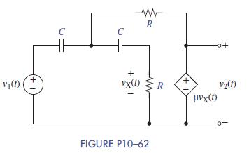
10–62 The circuit in Figure P10–62 is in the zero state.Use node-voltage equations to find the circuit determinant.Select values of R, C, and μ so that the circuit hasω0 = 10 krad=s and ζ = 0:5. (Hint: See Example 10–15.) V(f) 1+) w R C C HH vx(t) www FIGURE P10-62 +1 +o (1) V(1)
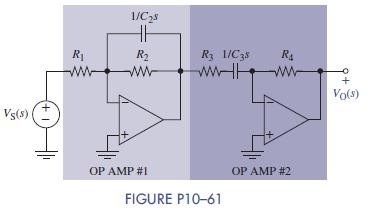
10–61 The two-OP AMP circuit in Figure P10–61 is a bandpass filter.(a) Your task is to design such a filter so that the lowfrequency cutoff is 2000 rad=s and the high-frequency cutoff is 200,000 rad=s. (Hint: See Example 10–16 and Exercise 10–18.)(b) Show that your design is correct using
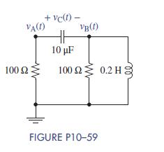
10–59 There is no external input in the circuit in Figure P10–59.(a) Find the zero-input node voltages vAðtÞ and vBðtÞ, and the voltage across the capacitor vCðtÞ when vCð0Þ = −5 V and iLð0Þ = 0A.(b) Use MATLAB to plot your results in (a).(c) Use Multisim to validate your results in
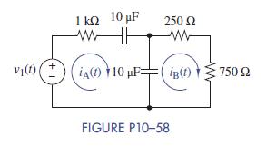
10–58 There is no initial energy stored in the circuit in Figure P10–58.(a) Find the zero-state mesh currents iAðtÞ and iBðtÞwhen v1ðtÞ = 10 e−2000tuðtÞ V.(b) Validate your answers using Multisim 1 10 250 ww ww V(t) (+ IA() 10 F iB (1) iB(f) 750 2 FIGURE P10-58
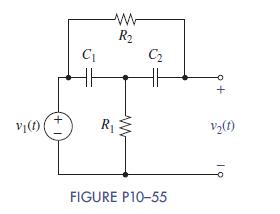
10–55 There is no initial energy stored in the bridged-T circuit in Figure P10–55.(a) Transform the circuit into the s domain and formulate mesh-current equations.(b) Use the mesh-current equations to find the s-domain relationship between the input V1ðsÞ and the output V2ðsÞ. v(t) C ww R C
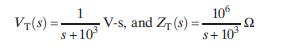
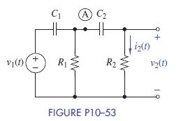
10–54 There is no initial energy stored in the circuit in Figure P10–53. The Thévenin equivalent circuit to the left of point A when a unit step is applied isSelect values for R2 and C2 such that the output transform is 1 VT(S) = s+103 V-s, and Zr(s) 106 S+10
10–53 There is no initial energy stored in the circuit in Figure P10–53.(a) Transform the circuit into the s domain and formulate node-voltage equations.(b) Solve these equations for V2ðsÞ in symbolic form.(c) Insert an OP AMP buffer at point A and solve for V2ðsÞ in symbolic form. How did
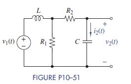
10–52 There is no initial energy stored in the circuit in Figure P10–51.(a) Transform the circuit into the s domain and formulate node-voltage equations.(b) Show that the solution of these equations for V2ðsÞ in symbolic form is(c) Identify the natural and forced poles of V2ðsÞ.(d) Find
10–51 There is no initial energy stored in the circuit in Figure P10–51.(a) Transform the circuit into the s domain and formulate mesh-current equations.(b) Show that the solution of these equations for I2ðsÞ in symbolic form is(c) Identify the poles and zeros of I2ðsÞ.(d) Find i2ðtÞ for
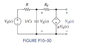
10–50 Find VOðsÞ in terms of the input and the elements for the zero state, dependent source circuit of Figure P10–50. Locate the natural poles and zeroes of the circuit. R www RF + + Vs(s) 1/Cs Vx(s) Vo(s) HVx(s) FIGURE P10-50
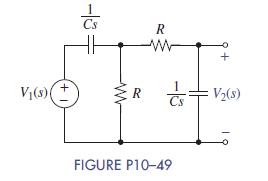
10–49 There is no initial energy stored in the circuit in Figure P10–49. Use circuit reduction to find the output network function V2ðsÞ=V1ðsÞ. Then select values of R and C so that the poles of the network function are approximately−2618 and −382 rad=s. V(s) +1 R ww w R = V2(8) FIGURE
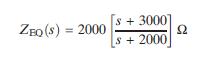
10–48 The equivalent impedance between a pair of terminals isA voltage vðtÞ = 10 e−10tuðtÞ is applied across the terminals.Find the resulting current response iðtÞ. ZEO(S)=2000 [S+3000] s+ 2000]
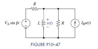
10–47 There is no initial energy stored in the circuit in Figure P10–47. Transform the circuit into the s domain and use superposition to findV s ð Þ. Identify the forced and natural poles in V s ð Þ. R www + VA sin t Lev(t) R w IBu(t) FIGURE P10-47
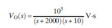
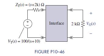
10–46 The Thévenin equivalent shown in Figure P10–46 needs to deliverto a 2-kΩ load. Design an interface to allow that to occur. 10 Vo(s)= s+2000) (s+10) V-s
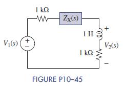
10–45 Find the required impedance ZXðsÞ that needs to be inserted in series as shown in Figure P10–45 to make the output voltage equal to ||V2(8)= s(s+1000) $+2000s+1061(s)
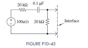
10–43 The circuit in Figure P10–43 is in the zero state. Find the Thévenin equivalent to the left of the interface. 20 0.1 ww HH + 100u(t) 20 k Interface FIGURE P10-43
Showing 300 - 400
of 7343
1
2
3
4
5
6
7
8
9
10
11
12
13
14
15
Last
Step by Step Answers