New Semester
Started
Get
50% OFF
Study Help!
--h --m --s
Claim Now
Question Answers
Textbooks
Find textbooks, questions and answers
Oops, something went wrong!
Change your search query and then try again
S
Books
FREE
Study Help
Expert Questions
Accounting
General Management
Mathematics
Finance
Organizational Behaviour
Law
Physics
Operating System
Management Leadership
Sociology
Programming
Marketing
Database
Computer Network
Economics
Textbooks Solutions
Accounting
Managerial Accounting
Management Leadership
Cost Accounting
Statistics
Business Law
Corporate Finance
Finance
Economics
Auditing
Tutors
Online Tutors
Find a Tutor
Hire a Tutor
Become a Tutor
AI Tutor
AI Study Planner
NEW
Sell Books
Search
Search
Sign In
Register
study help
business
systems analysis and design
The Analysis And Design Of Linear Circuits 8th Edition Roland E. Thomas, Albert J. Rosa, Gregory J. Toussaint - Solutions
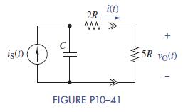
10–41 The circuit in Figure P10–41 is in the zero state. Use a Thévenin equivalent to find the s-domain relationship between the input ISðsÞ and the interface current IðsÞ. is(t) 2R ww i(t) ww FIGURE P10-41 5R vo(t)
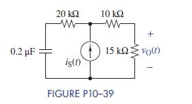
10–39 There is no energy stored in the capacitor in Figure P10–39 at t = 0: Transform the circuit into the s domain and use current division to find vOðtÞ when the input is iSðtÞ = 15 e−1000t uðtÞmA. Identify the forced and natural poles in VOðsÞ. 20 w 0.2 F is(t) 10 ww + 15 kovo(t)
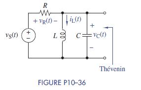
10–36 The initial conditions for the circuit in Figure P10–36 are vCð0Þ = 0 and iLð0Þ = I0. Transform the circuit into the s domain and use superposition and voltage division to find the zero-state and zero-input components of VCðsÞ. +1 vs(f) (+ R w +VR(I)-L(1) + C=vc(t) L C FIGURE P10-36
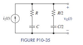
10–35 The circuit in Figure P10–35 is in the zero state. Find the s-domain relationship between the input I1ðsÞ and the output VOðsÞ. Identify the poles and the zeroes 4(0) www R FIGURE P10-35 www R/2 C12 vo(t)
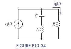
10–34 The circuit in Figure P10–34 is in the zero state. The s-domain relationship between the input I1ðsÞ and the output IRðsÞ is usually given as a ratio called a network function. Find IRðsÞ=I1ðsÞ. Identify the poles and the zeros. iR(f) i(1) C La R FIGURE P10-34
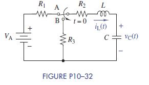
10–32 The switch in Figure P10–32 has been in position A for a long time and is moved to position B at t = 0:(a) Transform the circuit into the s domain and solve for ILðsÞ in symbolic form.(b) Repeat part (a) using MATLAB.(c) Find iLðtÞ for R1 = R2 = 500 Ω, R3 = 1 kΩ, L = 500mH, C = 0:15
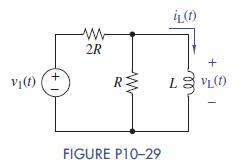
10–29 Transform the circuit in Figure P10–29 into the s domain and find: ILðsÞ, iLðtÞ, VLðsÞ, and vLðtÞ when v1ðtÞ = VA δðtÞ and iLð0Þ = IA. V(t) + www 2R iL(t) + R LVL (1) FIGURE P10-29 |
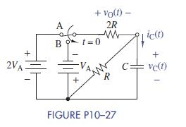
10–27 The switch in Figure P10–27 has been in position A for a long time and is moved to position B at t = 0. Transform the circuit into the s domain and solve for ICðsÞ, iCðtÞ, VOðsÞ, and vOðtÞ in symbolic form. 2VA + A + Vo(f)- 2R ww ic(t) B 1=0 + vc(t) R FIGURE P10-27 1
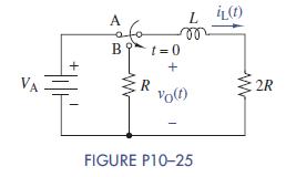
10–25 The switch in Figure P10–25 has been in position A for a long time and is moved to position B at t = 0. Transform the circuit into the s domain and solve for ILðsÞ, iLðtÞ, VOðsÞ, and vOðtÞ in symbolic form. VA A R 1=0 + LiL(t) m Vo(f) ww FIGURE P10-25 2R
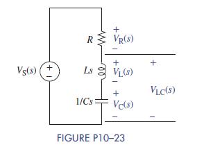
10–23 If the input to the RLC circuit of Figure P10–23 is vSðtÞ = uðtÞ:(a) Find the output voltage transform across each element.(b) Compare the three outputs with regard to their respective poles and zeros.(c) Use the initial- and final-value theorems to determine the value of the voltage
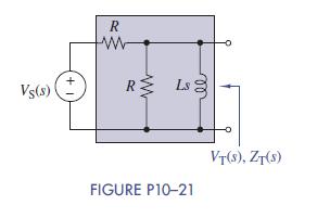
10–21 Find the Thévenin equivalent for the circuit in Figure P10–21. Then select values for R and L so that the Thévenin voltage has a pole at −24 krad=s. Vs(s) +1 R ww R Ls FIGURE P10-21 VT(S), ZT(S)
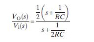
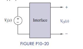
10–20 The interface circuit of Figure P10–20 needs to produce an output transform ofDesign an appropriate circuit Vo(s) 2 Vi(s) S+ S+ RC 1 2RC
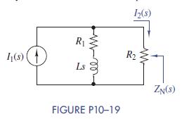
10–19 For the circuit of Figure P10–19:(a) Use current division to find I2ðsÞ.(b) Use the lookback method to find ZNðsÞ.(c) If I1ðsÞ is equal to IA=s, find the poles and zeroes of I2ðsÞ and identify the natural and the forced poles 12(s) 1(s) R Ls R FIGURE P10-19 ZN(S)
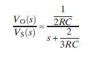
10–18 A load resistor RL = R is connected across the output in Figure P10–17. Show that the network function (in this case the ratio of the output to the input) is 1 Vo(s) 2RC Vs(s) S+ 2 3RC
10–17 For the circuit of Figure P10–17:(a) Use voltage division to find VOðsÞ.(b) Use the lookback method to find ZTðsÞ. www w R R Vs(s) 1/Cs Vo(s) ZT(s) FIGURE P10-17
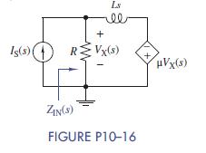
10–16 For the dependent circuit in Figure P10–16, select values of R, L, and μ, so that ZINðsÞ has a pole at s = −500 rad=s. + Ls ee Is(s)RVx(s) ZIN(S) FIGURE P10-16 HVx(s)
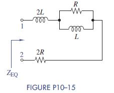
10–15 Find the equivalent impedance between terminals 1 and 2 in Figure P10–15. Select values of R and L so that ZEQðsÞ has a pole at s = −3:3 krad=s. Locate the zeroes of ZEQðsÞ for your choice of R and L. 2L R www 20 ZEQ 000 2R w L FIGURE P10-15
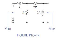
10–14 For the two-port circuit of Figure P10–14:(a) Find ZEQ1ðsÞ and ZEQ2ðsÞ, and express each impedance as a rational function and locate its poles and zeroes.(b) Select values of R and L to place a pole at −1 kHz. w 2R 2L ww 1 2 L R - ZEQI ee FIGURE P10-14 ZEQ2
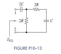
10–13 For the circuit of Figure P10–13:(a) Find and express ZEQðsÞ as a rational function and locate its poles and zeroes.(b) If its poles were located at −20 krad=s and zero, where would the poles move to if the value of R was reduced to half of its current value? 2 2C 2R 2R ww ZEQ FIGURE
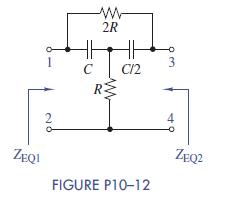
10–12 Find ZEQ1ðsÞ and ZEQ2ðsÞ for the bridge-T circuit in Figure P10–12. Express each impedance as a rational function and locate its poles and zeroes. www 2R HH C12 ww 1 2 C R 3. ZEQI FIGURE P10-12 4 ZEQ2
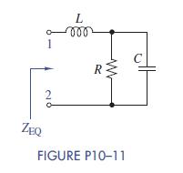
10–11 For the circuit of Figure P10–11:(a) If R = 560 Ω, L= 1 H, and C = 0:5 μF locate the poles and zeroes of ZEQðsÞ?(b) If we were to increase the resistance to 10 kΩ, how would the poles and zeroes change? L 000 2 R ZEQ FIGURE P10-11
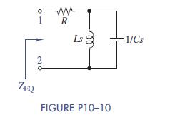
10–10 For the circuit of Figure P10–10:(a) Find and express ZEQðsÞ as a rational function and locate its poles and zeroes.(b) If R = 15kΩ, select values of L and C to locate poles at± j200 krad=s. Where are the resulting zeroes? ww 1 R 20 ZEQ Ls 1/Cs FIGURE P10-10
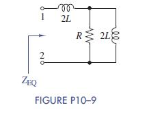
10–9 For the circuit of Figure P10–9:(a) Find and express ZEQðsÞ as a rational function and locate its poles and zeroes.(b) Select values of R and L to locate a pole at −15 krad=s.Where are the resulting zeroes? m 2L R2L 20 ZEQ FIGURE P10-9
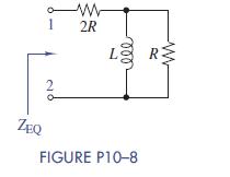
10–8 For the circuit of Figure P10–8:(a) Find and express ZEQðsÞ as a rational function and locate its poles and zeroes.(b) Select values of R and L to locate a pole at −330 rad=s.Where is the resulting zero? w 1 2R 20 ZEQ LR FIGURE P10-8
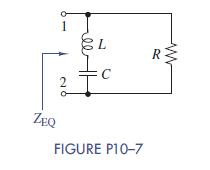
10–7 For the circuit of Figure P10–7:(a) Find and express ZEQðsÞ as a rational function and locate its poles and zeroes.(b) If R = 1kΩ and C = 0:1 μF, select a value of L to locate zeroes at ± j10 krad=s.(c) Where are the poles located once you have selected the inductor in part (b)? ZEQ 2
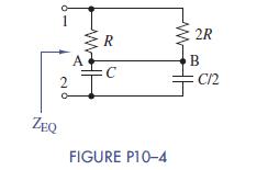
10–4 For the circuit of Figure P10–4:(a) Find and express ZEQðsÞ as a rational function and locate its poles and zeroes.(b) Select values ofR andC to locate a zero at s = −330 krad=s 2 A 2R R B C12 ZEQ FIGURE P10-4
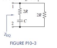
10–3 For the circuit of Figure P10–3:(a) Find and express ZEQðsÞ as a rational function and locate its poles and zeroes.(b) Select values of R and C to locate a pole at s = −22 krad=s. Where is the resulting zero? 1 2R ZEQ FIGURE P10-3 2R
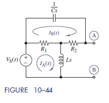
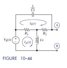
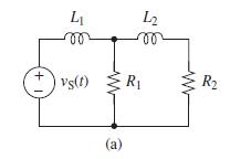
Formulate mesh-current equations for the circuit in Figure 10–44 when a resistor R3 is connected between nodes A and B. Assume that the initial conditions are zero. -10: IB(5) ww R V5(3) IA(S) ww R Ls 000 FIGURE 10-44 A B
(a) Formulate mesh-current equations for the circuit in Figure 10–44. Assume that the initial conditions are zero.(b) Find the circuit determinant.(c) Solve for the zero-state component of IBðsÞ. Cs -13= ww R In(s) IA(S)) 000 ww R Ls A B Vs(s) ( +1 FIGURE 10-44
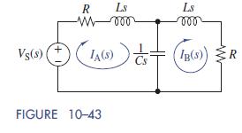
Formulate mesh current equations for the circuit in Figure 10–43 and solve for IBðsÞ in symbolic from. Locate the natural poles of the circuit for R=1 kΩ,C =4 μF, and L=1H. R Ls Ls eee-w Vs(s) IA(S) FIGURE 10-43 = (sex) eee
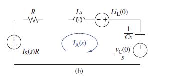
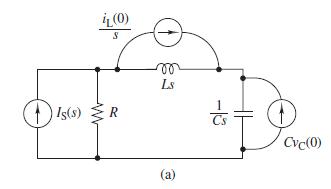
For the circuit in Figure 10–42(b), let ISðsÞ = 0:01=ðs + 500ÞA-s,L= 250mH,C = 1 μF, and R=1 kΩ. Use partial fraction expansion or MATLAB to solve for the zero-state component of iAðtÞ. R ww +1 Ls Li(0) ee -13 Is(s)R IA(S) vc(0) + S (b)
(a) Formulate mesh-current equations for the circuit in Figure 10–42(a).(b) Solve for the zero-input component of iAðtÞ for iLð0Þ = 0,υCð0Þ = 10 V, L= 250 mH,C =1 μF, and R=1 kΩ.(c) Use Multisim to simulate the circuit in Figure 10–42(b) and then validate your results by running a
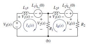
Solve for the zero-state components of IAðsÞ and IBðsÞ in Figure 10–41(b). Vs(s) 4 44 (0) Ls L24 (0) 00 + V(s) JA(S) V2(s) ee + + V3(S)- + + IB(S) V4(s) R2 (b)
(a) Formulate mesh-current equations for the circuit in Figure 10–41(a).(b) Solve for the zero-input component of IAðsÞ and IBðsÞ.(c) Find the zero-input responses iAðtÞ and iBðtÞ for R1 = 100 Ω, R2 = 200 Ω, L1 = 50 mH, and L2 = 100 mH. +1 L 12 ee el vs(t) R (a) R
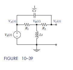
Formulate node-voltage equations for the circuit in Figure 10–39 and find the circuit determinant.Assume that the initial conditions are zero. -13= VA(S) VB(S) VC($) www ww R Vs(3) 000 Ls R2 FIGURE 10-39
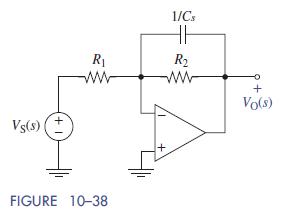
(a) For the s-domain circuit in Figure 10–38, solve for the zero-state output VOðsÞ in terms of a general input VSðsÞ.(b) Solve for the zero-state output when the input is a step functionυSðtÞ =VAuðtÞ V.(c) Select values of R1, R2, and C to produce a maximum gain of −100 and a pole at
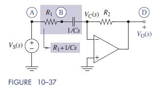
(a) For the s-domain circuit in Figure 10–37, solve for the zero-state output VOðsÞ in terms of a general input VSðsÞ.(b) Solve for the zero-state output υOðtÞ when the input is a unit step function υSðtÞ = uðtÞ V.(c) Select values of R1, R2, and C to produce a maximumgain of – 100
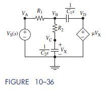
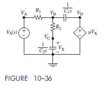
Consider the circuit in Figure 10–36. Select values for the various components to produce a pair of complex poles defined by ζ=0:5 and ω0 = 1 krad=s. To produce your design you must assume unity gain ðμ = 1Þ for the dependent source and that R1 =R2 =R. Vs(s) R VA VB I C Vp www R +1 + Vc +
The s-domain circuit in Figure 10–36 is to be designed to produce a pair of complex poles defined by ζ=0:5 and ω0 = 1000 rad=s. To simplify production the design will use equal element values R1 =R2 =R and C1 =C2 =C. Select the values of R, C, and the gain μ so that the circuit has the desired
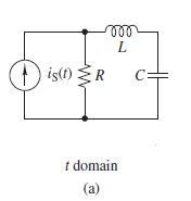
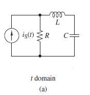
For the circuit of Figure 10–32(a), find the zero-state current transforms through each passive element. 000 L is(t) R C I domain (a)
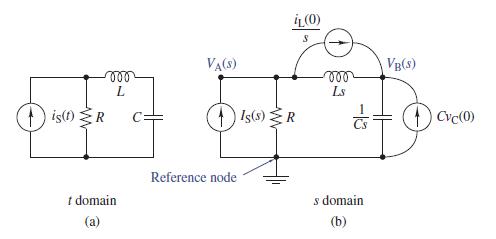
For the circuit of Figure 10–32, do the following:(a) Solve the node-voltage equations from Example 10–13 and identify the zero-state and zero-input responses.(b) Solve for the zero-state components of the waveforms υAðtÞ and υBðtÞ when R= 1 kΩ,C = 0:2 μF,L= 500mH, and iSðtÞ =
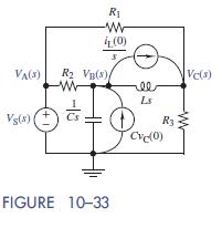
Using the nodes identified, write a set of node-voltage equations for the circuit of Figure 10–33. VA(3) V5(3) R ww 4(0) R Va(s) ww VC(3) ee -13 +- FIGURE 10-33 Ls Cvc(0) R3
Formulate s-domain node-voltage equations for the circuit in Figure 10–32(a). 000 L is(t) R C: I domain (a)
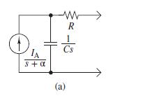
Find the Norton and the Thévenin equivalents of the s-domain circuits in Figure 10–30 ww R A Cs 10+ S (a)
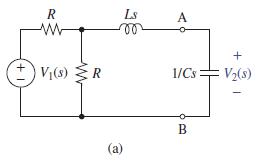
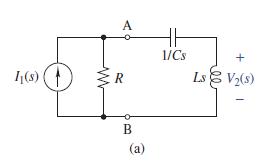
The circuit in Figure 10–29(a) is in the zero state. Use a Thévenin equivalent to find the s-domain relationship between the input V1ðsÞ and the output V2ðsÞ R www V(s) R Ls A + 1/Cs V(8) (a) B
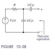
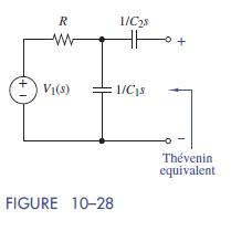
The circuit in Figure 10–28 has a 1-MΩ resistive load connected across the output. If C1 = C2 = 1μF and R = 10kΩ, find the location of the poles and zeroes of VOðsÞ=V1ðsÞ. (+1) R w 1/C28 HH V(s) 1/C1s Thvenin FIGURE 10-28 equivalent
The circuit of Figure 10–28 is in the zero state.(a) Find the Thévenin equivalent circuit that the load sees.(b) Find the Norton equivalent of the same circuit +1 R 1/C28 w V(s) 1/Cs Thvenin FIGURE 10-28 equivalent
The circuit in Figure 10–27(a) is in the zero state. Use a source transformation and voltage division to find the s-domain relationship between the input I1ðsÞ and the output V2ðsÞ. 1(s) R A 1/Cs Ls V(s) www B (a)
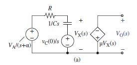
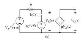
For the circuit of Figure 10–25(a), let the input voltage VSðsÞ =VA=s, and use superposition to find the zero-state and the zero-input components of the output. Identify the forced and natural poles. Then show that υOðtÞ is the same as that found in Example 10–3. R w 1/Cs + + Vo(s) Vx(s)
A transformed dependent-source circuit is shown in Figure 10–25(a). The capacitor has an initial voltage of VB V. Use superposition to find the zero-state and zero-input responses. Combine the results to find the total response transform VOðsÞ. Then use the total response components to find the
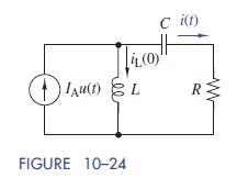
The initial conditions for the circuit in Figure 10–24 are υCð0−Þ = 0 and iLð0−Þ = I0.Transform the circuit into the s domain and find the zero-state and zero-input components of I s ð Þ. IAu(t) L (0)' C i(t) R FIGURE 10-24
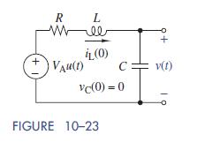
The initial conditions for the circuit in Figure 10–23 are υCð0−Þ = 0 and iLð0−Þ = I0. Transform the circuit into the s domain and find the zero-state and zero-input components of V s ð Þ. R L wee iL(0) +1. VAu(t) v(t) vc(0)=0 FIGURE 10-23
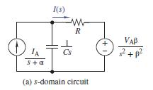
Use superposition to find the zero-state component of IðsÞ in the s-domain circuit shown in Figure 10–22(a). I(s) ww R (+1) IA Cs (a) s-domain circuit VAB 3+12
The switch in the circuit of Figure 10–21(a) has been closed for a long time. At t = 0 the switch is suddenly opened.(a) Find the transform IRðsÞ for the current through the resistor.(b) Select values of R, L, and C so that the current reaches at least 63% of its final value in 100 ms or less.
The switch in Figure 10–21(a) has been open for a long time and is closed at t =0(a) Transform the circuit into the s domain.(b) Find the zero-state and zero-input components of VðsÞ.(c) Find υðtÞ for IA = 1 mA,L= 2H,R=1:5 kΩ, and C =1=6 μF. IA t=0 RC L (a) I domain v(t)
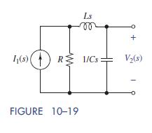
In Figure 10–19 find the network function relating the output V2ðsÞ to the input V1ðsÞ. Ls m + 11(5) R 1/Cs V(3) FIGURE 10-19
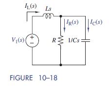
There is no initial energy stored in the circuit in Figure 10–18. Find the network functions relating IRðsÞ to V1ðsÞ and ICðsÞ to V1ðsÞ (s) Ls m 1+1 V(s) (+ IR(S) Ic(s) R 1/Cs FIGURE 10-18
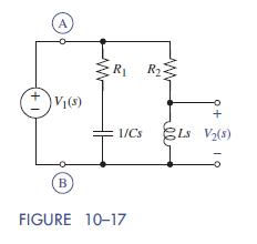
The inductor current and capacitor voltage in Figure 10–17 are zero at t =0.(a) Find the equivalent impedance between terminals A and B.(b) Solve for the output voltage transform V2ðsÞ in terms of the input voltage V1ðsÞ. (A) V(s) R B R2- + 1/Cs LS V2(8) FIGURE 10-17
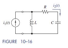
The circuit of Figure 10–16 is in the zero state.(a) Find the output current transform I2ðsÞ.(b) If R=1 kΩ, select values of L and C such that I2ðsÞ has two identical poles at −5000 rad=s. R i2(t) ww i(t) L C FIGURE 10-16
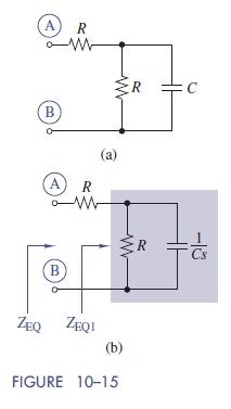
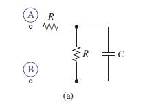
For Figure 10–15, select values of R and C so the ZEQðsÞ has a pole at s = −10,000: Use standard values from the inside rear cover. Under this design where is the zero located? A R w www R B (a) A R w B ww C -13 R ZEQ ZEQI (b) FIGURE 10-15
In a circuit analysis problem we are required to find the poles and zeros of a circuit.In circuit design we are required to adjust circuit parameters to place the poles and zeros at specified s-plane locations. This example is a simple pole-placement design problem.(a) Transform the circuit in
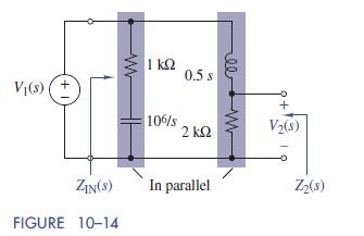
For the Figure 10–14, find the following:(a) The impedance Z2ðsÞ seen looking into the V2ðsÞ terminals with the input source set to zero (short-circuited).(b) The poles and zeros of Z2ðsÞ?(c) The impedance Z2ðsÞ seen looking into the V2ðsÞ terminals with the input source removed
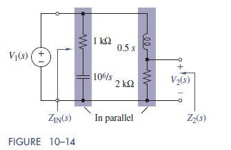
Consider the s-domain circuit in Figure 10–14.(a) Find the input impedance ZINðsÞ.(b) Find the ratio of the output V2ðsÞ to the input V1ðsÞ.(c) What are the poles and zeros of the input impedance and of V2ðsÞ=V1ðsÞ. V(s) (+ W 1 0.5 s 106/s 2 w V2(5) ZIN(S) In parallel Z(3) FIGURE
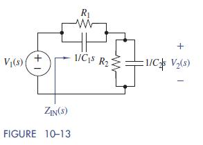
The circuit of Figure 10–13 is in the zero state.(a) Find the equivalent impedance ZINðsÞ that the source sees.(b) Find the output voltage V2ðsÞ. V(s) +1 R ww + 1/C1s R 1/C2 V(s) ZIN(S) FIGURE 10-13
The inductor current and capacitor voltage in Figure 10–12(a) are zero at t =0.(a) Transform the circuit into the s domain and find the equivalent impedance between terminals A and B.(b) Use voltage division to solve for the output voltage transform V2ðsÞ (A) L + V(t) R C B (a) V(1) 19
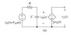
Replace the capacitor in the circuit of Figure 10–9(a) with an inductor, L, with an initial current of IBA. Find υOðtÞ and identify the forced and natural responses R w + C vx(f) vo(t) vs(t)=Vu(f) (1)
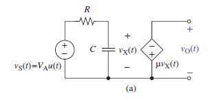
Find the output υOðtÞ for the dependent-source circuit shown in Figure 10–9(a). The capacitor has an initial voltage of VBV. R w C vx(t) vs(t)=Vu(t) (1) + vo(t)
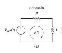
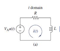
The source of the t-domain circuit of Figure 10–8(a) is suddenly turned off. Use Laplace techniques to solve for the voltage across the resistor υRðtÞ. VAu(t) +1 t domain R www i(t) (a) L
(a) Transform the circuit in Figure 10–8(a) into the s domain.(b) Solve for the current transform IðsÞ.(c) Perform the inverse transformation to find the waveform iðtÞ. VAu(t) +1 t domain R ww i(t) L (a)
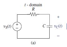
Transform the circuit of Figure 10–7(a) into the s domain and solve for the voltage υCðtÞ ifυSðtÞ =VAe−αtuðtÞV and υCð0Þ =V0. vs(t) t-domain R w (a) C vc(t)
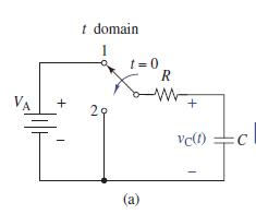
The switch in Figure 10–6(a) has been in position 1 for a long time and is moved to position 2 at t = 0. For t > 0, transform the circuit into the s domain and use Laplace transforms to solve for the voltage υCðtÞ t domain 1=0 R + VA 29 vc(1) (a)
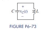
6–75 Air-Coil Inductor Design In a particular radio frequency (RF) application, you determine there is a need for a small inductor of 150 μH and rather than trying to order one and wait for it to arrive, you decide to wind it yourself. The applicable equation iswhere L is the inductance in μH,
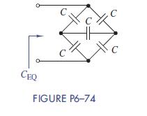
6–74 Equivalent Capacitance Bridge Find the equivalent capacitance of the capacitance bridge shown in Figure P6–74. (Hint: Use Node Analysis.) C. C C CEQ C FIGURE P6-74 C
In Section 6–1, Figure 6–2(c) shows an air-tunable capacitor as one example of the capacitor types. This type of device can vary its capacitance similar to how a potentiometer can vary its resistance.Changing the capacitance in a circuit can change the frequency at which it operates. Suppose we
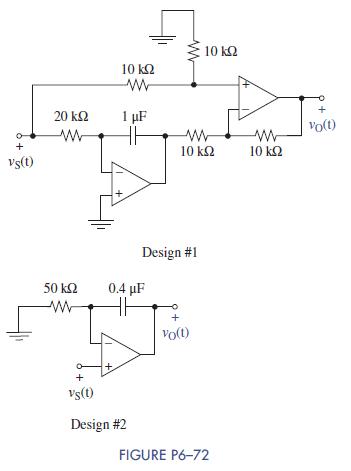
6–72 RC OP AMP Circuit Design An upgrade to one of your company’s robotics products requires a proportional plus integral compensator that implements the input–output relationshipThe input voltage vSðtÞ comes fromanOPAMP, and the output voltage vO(t) drives a 10-kΩ resistive load. Two
6–71 Analog Computer Solution Design an OP AMP circuit that solves the following secondorder differential equation for vOðtÞ. Solve for the response for vO(t) using Multisim. Caution: Avoid saturating the OP AMPs by distributing the gain across several OP AMPs. di 10-6d-vo (1) +10-3 dvo(t) + vo
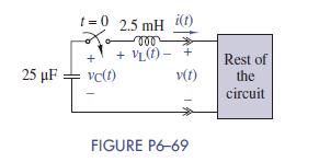
6–69 LC Circuit Response At t = 0 the switch in Figure P6–69 is closed and thereafter the voltage across the capacitor is vCðtÞ = (10 + 10;000t) e− 8000 t V Use MATLAB to solve all of the following problems.(a) Use the capacitor’s i – v characteristic to find the current iðtÞ for t
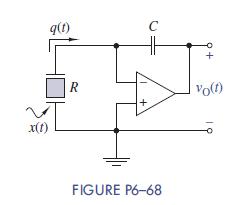
6–68 Piezoelectric Transducer Piezoelectric transducers (sensors) measure dynamic phenomena such as pressure and force. These phenomena cause stresses that “squeeze” a quantity of electric charge from piezoelectric material in the transducer (the term piezo means “squeeze”in Greek). The
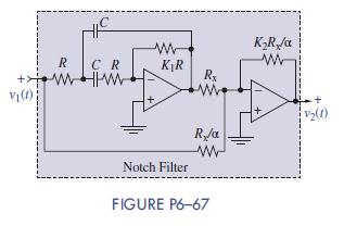
6–67 The OP AMP circuit in Figure P6–67 is a notch filter that will be studied later. Determine the circuit gain at dc and as the frequency approaches ∞ rad/s. CR ww V(1) R ww KR/ w KR Rx v(1) R/a www Notch Filter FIGURE P6-67
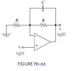
6–66 The OP AMP circuit in Figure P6–66 has a capacitor in its feedback loop. Determine the circuit gain at dc and as the frequency approaches ∞ rad/s C R w R ww + 0+ + vs(f) FIGURE P6-66 vo(t)
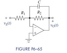
6–65 The OP AMP circuit in Figure P6–65 has a capacitor in its feedback loop. Determine the circuit gain at dc and as the frequency approaches ∞ rad=s. R vs(f) C R www + vo(t) FIGURE P6-65
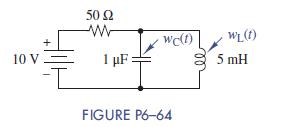
6–64 The circuit in Figure P6–64 is driven by 10-V dc source.Find the energy stored in the capacitor and inductor under dc conditions 10 V + 50 ww 1 F wc(t) WL (1) 5 mH FIGURE P6-64
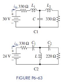
6–63 The circuits in Figure P6–63 are driven by dc sources. Find the current through the source under dc conditions. ide 330 2 Li 12 30 V C 330 C1 ide 3302 C w C 24 V L 220 2 C2 FIGURE P6-63
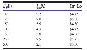
6–62 A switching power supply requires an inductor that can store at least 1 mJ of energy. A list of available inductors is shown below. Select the inductor that best meets the requirement. Consider both meeting the specifications and cost. Explain your choice. LuH) MAX(A) COST EACH 10 9.2 $4.75
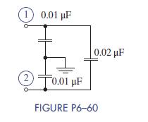
6–60 Figure P6–60 is the equivalent circuit of a two-wire feedthrough capacitor.(a) What is the capacitance between terminal 1 and ground when terminal 2 is open?(b) What is the capacitance between terminal 1 and ground when terminal 2 is grounded? 0.01 F 2 0.01 F 0.02 F FIGURE P6-60
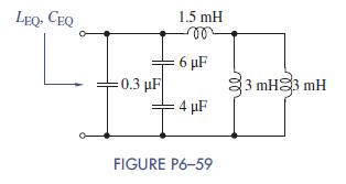
6–59 For the circuit in Figure P6–59, find an equivalent circuit consisting of one inductor and one capacitor. Select a value of an inductor and a capacitor from among the standard values in the inside rear cover to realize your result and connect them appropriately. LEQ, CEQ 1.5 mH m 6 F 0.3 F
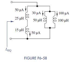
6–58 What is the equivalent inductance and initial current for the inductors shown in Figure P6–58? 50 1 30 A 100 A 25 pH 50 pH 100 pH 15 pH 1 wux 50 LEQ FIGURE P6-58
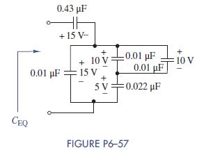
6–57 What is the equivalent capacitance and initial voltage for the capacitor bank shown in Figure P6–57? 0.43 F +15 V- 10 V +0.01 F 0.01 F 15 V 0.01 F 5V 0.022 uF CEQ FIGURE P6-57 + 10 V
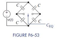
6–53 Use the lookback method to find the equivalent capacitance of the circuit shown in Figure P6–53. + v(t) C C C C CEQ FIGURE P6-53
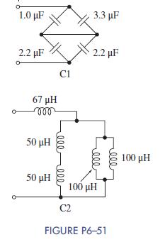
6–51 Find a single equivalent element for each circuit in Figure P6–51. 1.0 F 3.3 F 2.2 F 2.2 F 67 pH 000 50 pH C1 eee 000 50 pH 100 pH eee 100 pH C2 FIGURE P6-51
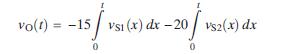
6–50 Design an RC circuit using only one OP AMP and only one capacitor that implements the input–output relationship dx-20/vs2(x) vo(t)=-15 vsi (x) dx-20 vs2(x) dx 0
6–49 Design an OP AMP circuit to solve the following differential equation: 1 dvs(t) 1 dvs(t). vo(t) = 10 vs(t) + + 10 dt 20 di
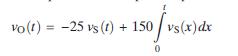
6–48 Draw a block diagram and then design an RC OP AMP circuit to implement the input–output relationship vo (1) = 25 vs (1) + 150 vs (x)dx
6–47 In this problem you will design an oscillator. The equation for your oscillator is(a) Draw a block diagram to solve your equation (vO(t)should be your output) using differentiators.(b) Draw a block diagram to solve your equation (vO(t)should be your output) using integrators.(c) Design a
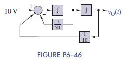
6–46 For the block diagram shown in Figure P6–46(a) Find the differential equation the block diagram represents.(b) Design an RC OP AMP circuit that implements the block diagram. 10 V- 50 FIGURE P6-46 10 vo(t)
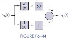
6–44 Design an RC OP AMP circuit to implement the block diagram in Figure P6–44 vs(f) d dt 50 vo(t) 50 J FIGURE P6-44
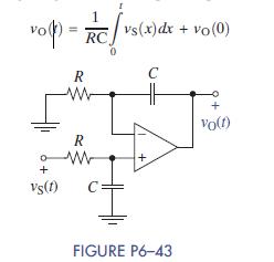
6–43 Show that the RC OP AMP circuit in Figure P6–43 is a noninverting integrator whose input–output relationship is 1 vo = RC R www vs(x)dx + vo(0) C + Vo(f) + Vs(f) R C + FIGURE P6-43
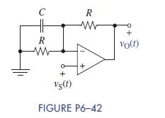
6–42 Find the input–output relationship of the RC OP AMP circuit in Figure P6–42. C R www + Vs(1) R www + FIGURE P6-42 + vo(t)
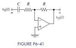
6–41 Find the input–output relationship of the RC OP AMP circuit in Figure P6–41. CR R wwwww + FIGURE P6-41 + Vo(t)
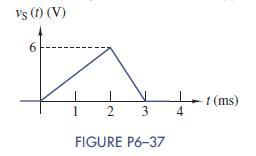
6–37 The OP AMP differentiator in Figure P6–35 with R = 33kΩ, C = 0:1 μF, and a VCC = 12 V has the input waveform shown in Figure P6–37. Sketch vOðtÞ for t > 0. Vs (f) (V) 6 -1 (ms) 1 2 3 4 FIGURE P6-37
Showing 400 - 500
of 7343
1
2
3
4
5
6
7
8
9
10
11
12
13
14
15
Last
Step by Step Answers