New Semester
Started
Get
50% OFF
Study Help!
--h --m --s
Claim Now
Question Answers
Textbooks
Find textbooks, questions and answers
Oops, something went wrong!
Change your search query and then try again
S
Books
FREE
Study Help
Expert Questions
Accounting
General Management
Mathematics
Finance
Organizational Behaviour
Law
Physics
Operating System
Management Leadership
Sociology
Programming
Marketing
Database
Computer Network
Economics
Textbooks Solutions
Accounting
Managerial Accounting
Management Leadership
Cost Accounting
Statistics
Business Law
Corporate Finance
Finance
Economics
Auditing
Tutors
Online Tutors
Find a Tutor
Hire a Tutor
Become a Tutor
AI Tutor
AI Study Planner
NEW
Sell Books
Search
Search
Sign In
Register
study help
business
systems analysis and design
The Analysis And Design Of Linear Circuits 7th Edition Roland E Thomas, Albert J Rosa, Gregory J Toussaint - Solutions
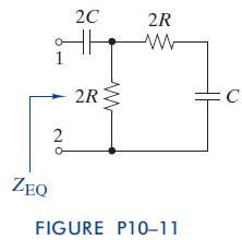
For the circuit of Figure P10–11:(a) Find and express ZEQ(s) as a rational function and locate its poles and zeros.(b) If its poles were located at 20 krad/s and zero, where would the poles move to if the value of R was reduced to 25%of its current value? 2C 2R w ww 1 2 2R ZEQ FIGURE P10-11 C
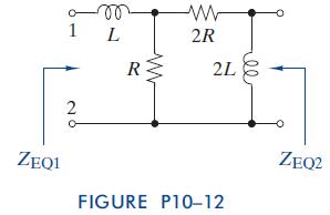
For the two-port circuit of Figure P10–12:(a) Find ZEQ1(s) and ZEQ2, and express each impedance as a rational function and locate its poles and zeros.(b) Select values of R and L to place a pole at 500 Hz. ZEQ1 2 m ww 1 L 2R R ww FIGURE P10-12 2L ZEQ2
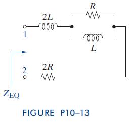
Find the equivalent impedance between terminals 1 and 2 in Figure P10–13. Select values of R and L so that ZEQ(s) has a pole at s ¼ 3000 rad/s. Locate the zeros of ZEQ(s) for your choice of R and L. 1 2 2L 000 2R R ww 000 L www ZEQ FIGURE P10-13
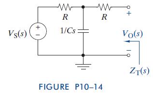
For the circuit of Figure P10–14:(a) Use voltage division to find VO(s).(b) Use the look-back method to find ZT(s). Vs(s) ww www R 1/Cs: R FIGURE P10-14 Vo(s) ZT(S)
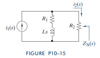
For the circuit of Figure P10–15:(a) Use current division to find I2(s).(b) Use the look-back method to find ZN(s). in(s) R1 Ls FIGURE P10-15 i2(s) R2 ZN(S)
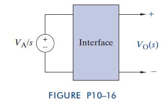
The circuit of Figure P10–16 needs to produce an output transform of VOðsÞ ¼ VAðRCs þ 1Þsð2RCs þ 1Þwhen the input is VA/s. Design an appropriate circuit. + VA/S Interface Vo(s) FIGURE P10-16
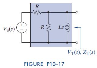
Find the Thevenin equivalent for the circuit in Figure P10–17. Then select values for R and L so that the Thevenin voltage has a pole at 12 krad/s. Vs(s) +1 R ww R Ls FIGURE P10-17 VT(S), ZT(S)
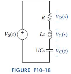
If the input to the RLC circuit of Figure P10–18 is vS(t) ¼u(t):(a) Find the output voltage transform across each element.(b) Compare the three outputs with regards to their respective poles and zeros.(c) Use the initial and final value theorems to determine the value of the voltage across each
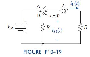
The switch in Figure P10–19 has been in position A for a long time and is moved to position B at t ¼ 0. Transform the circuit into the s domain and solve for IL(s), iL(t), VO(s), and vO(t) in symbolic form. VA + LiL(t) A B1=0 R + vo(t) FIGURE P10-19 ww R
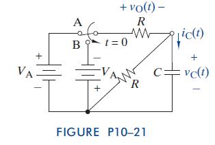
The switch in Figure P10–21 has been in position A for a long time and is moved to position B at t ¼ 0. Transform the circuit into the s domain and solve for IC(s), iC(t) VO(s), and vO(t) in symbolic form. A + vo(t) - R www BO t=0 ic(t) + VA C= vc(t) R FIGURE P10-21
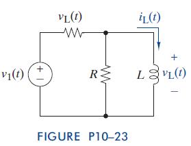
Transform the circuit in Figure P10–23 into the s domain and find: IL(s), iL(t) VL(s), and vL(t) when v1(t) ¼ VAu(t) and iL(0) ¼ IA. + V1(t) VL(t) ww iL(t) R ww + LVL(t) FIGURE P10-23
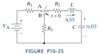
The switch in Figure P10–25 has been in position A for a long time and is moved to position B at t¼ 0.(a) Transform the circuit into the s domain and solve for IL(s) in symbolic form.(b) Repeat part (a) using MATLAB.(c) Find iL(t) for R1¼ R2 ¼ 500 V, R3 ¼ 1 kV, L ¼ 500 mH, C ¼ 0.2 mF, and
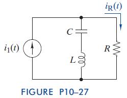
The circuit in Figure P10–27 is in the zero state. The s-domain relationship between the input I1(s) and the output IR(s) is usually given as a ratio called a network function. Find IR(s)/I1(s). Identify the poles and the zeros. i1(t) L iR(t) FIGURE P10-27 R www
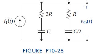
The circuit in Figure P10–28 is in the zero state. Find the s-domain relationship between the input I1(s) and the output VO(s). Identify the poles and the zeros. i1(t) W 2R www R vo(t) C C/2 FIGURE P10-28
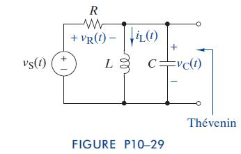
The initial conditions for the circuit in Figure P10–29 are vC(0) ¼ 0 and iL(0) ¼ I0. Transform the circuit into the s domain and use superposition and voltage division to find the zero-state and zero-input components of VC(s). vs(t) R w +VR(t) L(t) - L2 + C=vc(t) + I FIGURE P10-29 Thvenin
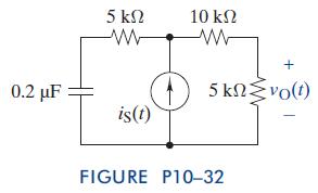
There is no energy stored in the capacitor inFigure P10–32 at t¼0.Transform the circuit into the sdomain and use current division to find vO(t)when the input is iS(t) ¼ 5 e500tu(t) mA.Identify the forced and natural poles in VO(s). 5 w 0.2 F is(t) 10 ww + 5 kvo(t) FIGURE P10-32
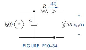
The circuit in Figure P10–34 is in the zero state. Use a Thevenin equivalent to find the s-domain relationship between the input IS(s) and the interface current I(s). is(t) R w i(t) C FIGURE P10-34 + 5R vo(t)
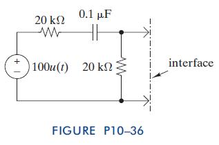
The circuit in Figure P10–36 is in the zero state. Find the Thevenin equivalent to the left of the interface. + 20 ww 0.1 F HH 100u(t) 20 k2 interface FIGURE P10-36
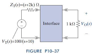
The Thevenin equivalent shown in Figure P10–37 needs to deliver VOðsÞ ¼ 50000ðs þ 1500Þðs þ 10Þ V-s to a 1-kV load. Design an interface to allow that to occur. ZT(S)=(s+2k) + + Interface 1 kVo(s) VT(S)=100/(s+10) FIGURE P10-37
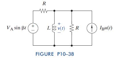
There is no initial energy stored in the circuit in Figure P10–38. Transform the circuit into the s domain and use superposition to find V(s). Identify the forced and natural poles in V(s). VA sin t 1+ R w + Lev(t) FIGURE P10-38 w R IBu(t)
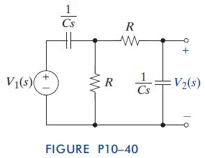
There is no initial energy stored in the circuit in Figure P10–40. Use circuit reduction to find the output network function V2(s)/V1(s). Then select values of R and C so that the poles of the network function are approximately2618 and 382 rad/s. V(s) 1 + Cs R w w R V(s) Cs FIGURE P10-40
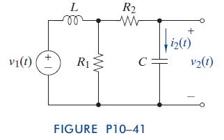
There is no initial energy stored in the circuit in Figure P10–41.(a) Transform the circuit into the s domain and formulate mesh-current equations.(b) Show that the solution of these equations for I2(s) in symbolic form is I2ðsÞ ¼ IBðsÞ ¼ R1CsV1ðsÞðR1 þ R2ÞLCs2 þ ðR1R2C þ LÞs þ
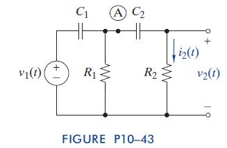
There is no initial energy stored in the circuit in Figure P10–43.(a) Transform the circuit into the s domain and formulate node-voltage equations.(b) Solve these equations for V2(s) in symbolic form.(c) Insert an OPAMP buffer at point A and solve for V2(s)in symbolic form. How did inserting the
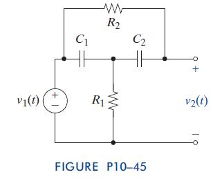
There is no initial energy stored in the bridged-T circuit in Figure P10–45.(a) Transform the circuit into the s domain and formulate mesh-current equations.(b) Use the mesh-current equations to find the s-domain relationship between the input V1(s) and the output V2(s). C1 ww R C v1(t) + | R1
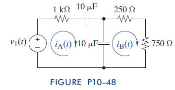
There is no initial energy stored in the circuit in Figure P10–48.(a) Find the zero-state mesh currents iA(t) and iB(t) when v1(t) ¼ 50 e1000tu(t) V.(b) Validate your answers using OrCAD. v1(t) + 1 10 F 250 (A(t) 10 FiB(t)750 2 FIGURE P10-48
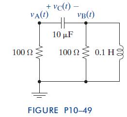
There is no external input in the circuit in Figure P10–49.(a) Find the zero-input node voltages vA(t) and VB(t), and the voltage across the capacitor vC(t)when vC(0)¼5 Vand iL(0) ¼ 0 A.(b) Use MATLAB to plot your results in (a).(c) Use OrCAD to validate your results in (a).(d) Compare
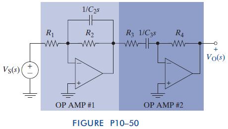
The two-OPAMP circuit in Figure P10–50 is a bandpass filter.(a) Yourtaskis todesignsucha filter so that the low-frequency cutoff is 1000 rad/s and the high-frequency cutoff is 100,000 rad/s. (Hint: See Example 10–16 and Exercise 10–18.)(b) Show that your design is correct using OrCAD. Vs(s) |
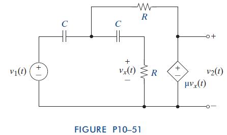
The circuit in Figure P10–51 is in the zero state. Use node-voltage equations to find the circuit determinant. Select values ofR,C, andm so that the circuit has v0¼5 krad/s and z ¼ 0.707. vi(t) +1 C C w R + Vx(t) R FIGURE P10-51 + o+ . (1) v2(t) -
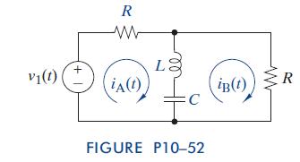
The circuit in Figure P10–52 is in the zero state. Use mesh-current equations to find the circuit determinant.Select values of if, R, L, and C so that the circuit has v0 ¼10 krad/s and z ¼ 1. v1(t) 1 + R w iA(t) L2 iB(t) C FIGURE P10-52 w R
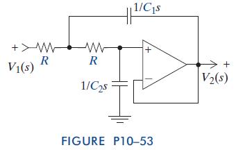
The OPAMP circuit in Figure P10–53 is in the zero state. Use node-voltage equations to find the circuit determinant.Select values of R, C1, and C2 so that the circuit has v0 ¼ 10 krad/s and z ¼ 1. W
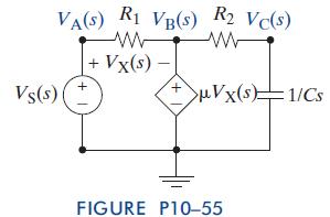
Three node voltages are shown in Figure P10–55.(a) Explain why only one of the node voltages is independent.(b) Write a node voltage equation in the independent node voltage.(c) If VC(s) is the circuit’s output, find the output-input ratio or network function, VC(s)/VS(s). VA(S) R1 VB(S) R2
Three mesh currents are shown in Figure P10–56.(a) Explain why only two of these mesh currents are independent.(b) Write s-domain mesh-current equations in the two independent mesh currents. Vs(s) 1+ Cs www R IA(s) Ic(s) 000 ww Ls R IB(s) Blx(s) Ix(s) FIGURE P10-56
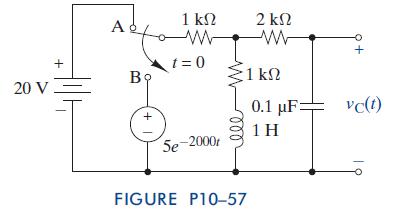
The switch in Figure P10–57 has been in position A for a long time and is moved to position B at t ¼ 0.(a) Write an appropriate set of node-voltage or meshcurrent equations in the s-domain.(b) Use MATLAB to solve for VC(s) and vC(t). Also using MATLAB, plot vC(t) and the exponential source on
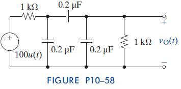
There is no energy stored in the circuit in Figure P10–58 at t ¼ 0. Transform the circuit into the s domain and solve for VO(s) and vO(t) 1 www 0.2 F 1 k vo(t) 0.2 F 0.2 F 100u(t) FIGURE P10-58
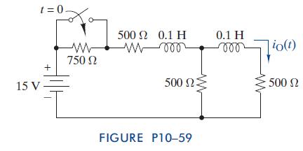
The switch in Figure P10–59 has been open for a long time and is closed at t ¼ 0. Transform the circuit into the s domain and solve for IO(s) and iO(t) t=0. 500 0.1 0.1 H www 750 --000 io(t) 15 V 500 - 500 FIGURE P10-59
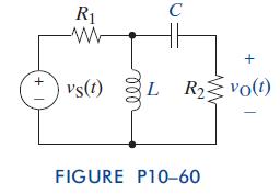
There is no initial energy stored in the circuit in Figure P10–60.(a) Transform the circuit into the s domain and solve for VO(s) in symbolic form.(b) If R1 ¼ R2 ¼ 500 V, select values of L and C to produce z ¼ 0.707 and v0 ¼ 707 rad/s. (Hint: Try values of L first, i.e., 100 mH, 200 mH,
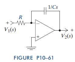
With the circuit in the zero state, the input to the integrator shown in Figure P10–61 is v1(t) ¼ cos1000t V.The desired output is v2(t) ¼ sin 1000t V. Use Laplace to select values of R and C to produce the desired output. If the capacitor had 10 V across it at t ¼ 0, how would that affect the
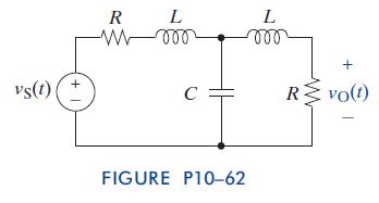
Show that the circuit in Figure P10–62 has natural poles at s ¼ 4/RC and s ¼ 2/RC j2/RC when L ¼ R2C/4. vs(t) + R L L -000 + C R vo(t) FIGURE P10-62
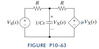
Find the range of the gain m for which the circuit’s output VX(s) in Figure P10–63 is stable (i.e., all poles are in the left hand side of the s plane.) Vs(s) R www + R www 1/Cs=Vx(s) >Vx(s) FIGURE P10-63
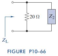
Design a Load Impedance In order to match the Thevenin impedance of a source, the load impedance in Figure P10–66 must be ZLðsÞ ¼ sþ5 sþ10:(a) What impedance Z2(s) is required?(b) How would you realize Z2(s) using only resistors, inductors, and/or capacitors? (Hint: Write ZL(s) as a sum of
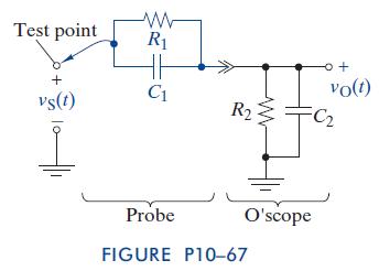
RC Circuit Analysis and Design The RC circuits in Figure P10–67 represent the situation at the input to an oscilloscope. The parallel combination of R1 and C1 represent the probe used to connect the oscilloscope to a test point. The parallel combination of R2 and C2 represent the input impedance
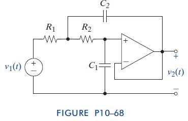
s-domain OP AMP Circuit Analysis The OP AMP circuit in Figure P10–68 is in the zero-state.Transformthe circuit into the s-domain and use the OPAMP circuit analysis techniques developed in Section 4–4 to find the relationship between the input V1(s) and the output V2(s). V1(t) R R ww www C= +1 +
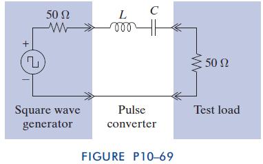
Pulse Conversion Circuit The purpose of the test setup in Figure P10–69 is to deliver damped sine pulses to the test load. The excitation comes from a 1-Hz square wave generator. The pulse conversion circuit must deliver damped sine waveforms with z 10 krad/s to 50-V and 600-V loads. The
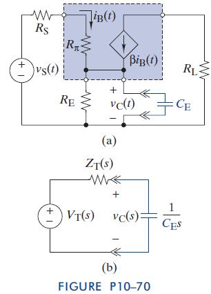
By-Pass Capacitor Design In transistor amplifier design, a by-pass capacitor is connected across the emitter resistor RE to effectively short out the emitter resistor at signal frequencies. This then, improves the gain of the transistor for the desired ac signals. The circuit in Figure P10–70(a)
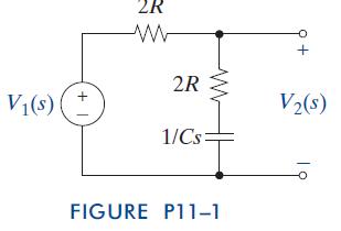
Find the driving point impedance seen by the voltage source in Figure P11–1 and the voltage transfer function TV(s) ¼ V2(s)/V1(s). V(s) + | 2R ww 2R 1/Cs: FIGURE P11-1 V2(s)
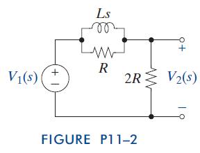
Find the driving point impedance seen by the voltage source in Figure P11–2 and the voltage transfer function TV(s) ¼ V2(s)/V1(s). V(s) 1 + Ls R 2R V(s) FIGURE P11-2
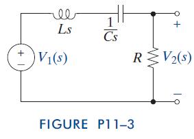
Find the driving point impedance seen by the voltage source in Figure P11–3 and the voltage transfer function TV(s) ¼ V2(s)/V1(s). + 1 + Ls V(s) Cs RV2(s) FIGURE P11-3
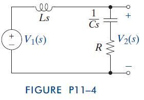
Find the driving point impedance seen by the voltage source in Figure P11–4 and the voltage transfer function TV(s) ¼ V2(s)/V1(s). el Ls 13 Cs V(s) V2(s) R + I FIGURE P11-4
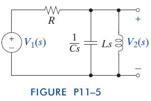
Find the driving point impedance seen by the voltage source in Figure P11–5 and the voltage transfer function TV(s) ¼ V2(s)/V1(s). +1 w R V(s) 113 Ls V(s) FIGURE P11-5
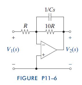
Find the driving point impedance seen by the voltage source in Figure P11–6 and the voltage transfer function TV(s) ¼ V2(s)/V1(s). + V(s) 1/Cs R 10R www w FIGURE P11-6 + V2(s)
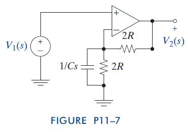
Find the driving point impedance seen by the voltage source in Figure P11–7 and the voltage transfer function.TV(s) ¼ V2(s)/V1(s). + V(s) + + 2R V2($) w 1/Cs 2R FIGURE P11-7
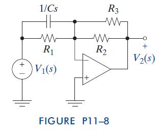
Find the driving point impedance seen by the voltage source in Figure P11–8 and the voltage transfer function TV(s) ¼ V2(s)/V1(s). 1/Cs HH R3 W w w + R R2 V(s) + V(s) + FIGURE P11-8
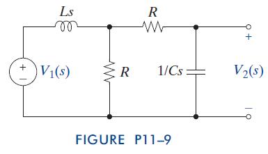
Find the voltage transfer function TV(s) ¼ V2(s)/V1(s) in Figure P11–9. Ls R m www V(s) R 1/Cs V2(s) + I FIGURE P11-9
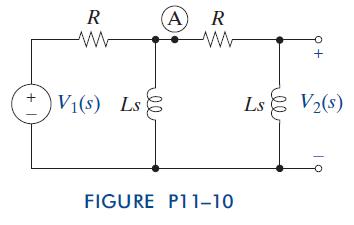
Find the driving point impedance seen by the voltage source in Figure P11–10 and the voltage transfer function TV(s) ¼ V2(s)/V1(s). Insert a follower at A and repeat. + 1 R w (A) V(s) Ls R w + Ls V(s) FIGURE P11-10 10
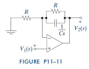
Find the voltage transfer function TV(s) ¼ V2(s)/V1(s) in Figure P11–11. Select values of R and C so that TV(s)has a pole at s ¼ 100 krad/s. R w R V(s) + 113 Cs + V2(s) FIGURE P11-11
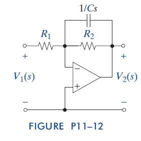
Find the voltage transfer function TV(s) ¼ V2(s)/V1(s) in Figure P11–12. Select values of R1, R2, and C so that TV(s) has a pole at s ¼ 250 krad/s and R2/R1 ¼ 100. 1/Cs R R W ww + V($) V(s) + FIGURE P11-12
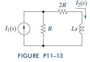
Find the current transfer function TI(s) ¼ I2(s)/I1(s)in Figure P11–13. Select values of R and L so that TI(s) has a pole at s ¼ 377 rad/s. 11(s) ww 2R 12(s) www R Ls FIGURE P11-13 ee
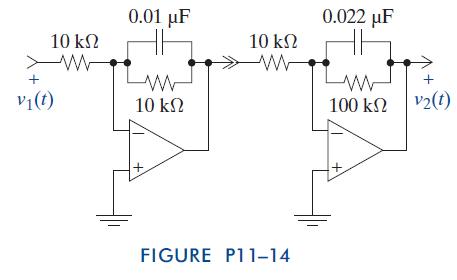
Find the voltage transfer function TV(s) ¼ V2(s)/V1(s) of the cascade connection in Figure P11–14. Locate the poles and zeros of the transfer function. + v1(t) 10 w 0.01 F 10 ww W 10 + FIGURE P11-14 0.022 F ww + 100 2(1)
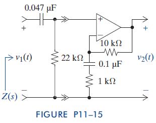
Find the voltage transfer function TV(s) ¼ V2(s)/V1(s) of the cascade connection in Figure P11–15. Locate the poles and zeros of the transfer function. 0.047 uF + + 10 w + V(t) 22 v2(t) 0.1 F 1 Z(s) FIGURE P11-15
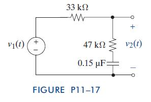
Find the impulse response at v2(t) in Figure P11–17. Find the circuit’s step response. V(1) + 33 ww 47 0.15 F: FIGURE P11-17 v2(t)
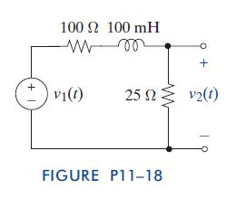
Find v2(t) in Figure P11–18 when v1(t) ¼ d(t). Repeat for v1(t) ¼ u(t). 1 + 100 2 100 mH + v1(t) 25 v2(t) FIGURE P11-18
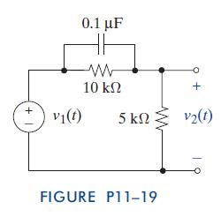
Find v2(t) in Figure P11–19 when v1(t) ¼ d(t). Repeat for v1(t) ¼ u(t). 1 + 0.1 F w 10 + v1(t) 5 kv(1) FIGURE P11-19
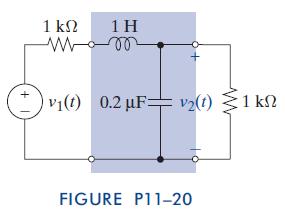
Find h(t) and g(t) for the circuit in Figure P11–20. 1 1 H www v1(t) 0.2 Fv2(t) 1 ks + FIGURE P11-20
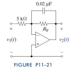
Find h(t) and g(t) for the circuit in Figure P11–21 if RF ¼ 100 kV. + v1(t) 5 w 0.02 F HH w RF FIGURE P11-21 + v2(t)
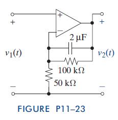
Find v2(t) in Figure P11–23 when v1(t) ¼ d(t). Repeat for v1(t) ¼ u(t). + v1(t) 2 F ww 100 50 V2(t) FIGURE P11-23
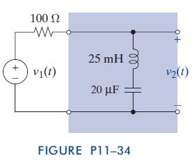
The circuit in Figure P11–34 is in the steady state with v1(t) ¼ 5 cos 1414.21t V. Find v2SS(t). Repeat for v1(t) ¼ 5 cos 1 kt V. And without doing any calculations, repeat for v1(t) ¼ 5 V. 100 ww 25 mH v(t) v2(t) 20 F FIGURE P11-34
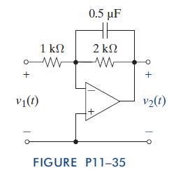
The circuit in Figure P11–35 is in the steady state with v1(t)¼ 10 cos 500t V. Find v2SS(t). Repeat for v1(t) ¼ 10 cos 1 kt V, and for v1(t) ¼ 10 cos 10 kt V. Where is the pole located? + v1(t) 1 W 0.5 F 2 www + + FIGURE P11-35 v2(t)
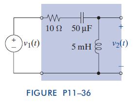
The circuit in Figure P11–36 is in the steady state with v1(t) ¼ 25 cos 2000t V. Find v2SS(t). Repeat for v1(t) ¼ 25 cos 10 kt V . Where are the poles located? + I w v1(t) 10 50 5 mH V2(1) FIGURE P11-36
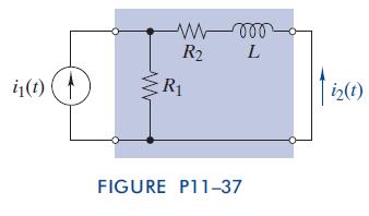
The circuit in Figure P11–37 is in the steady state with i1(t) ¼ 10 cos 50kt mA, R1 ¼ 100 V, R2 ¼ 400 V, and L ¼100 mH. Find i2SS(t). Repeat for i1(t) ¼ 10 cos 5kt mA.Where is the pole located? R L i1(t) R1 i2(t) FIGURE P11-37
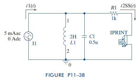
The circuit in Figure P11–38 is in the steady state with i1(t) ¼ 5 cos 1000t mA, R ¼ 1 kV, L, ¼ 2H, and C ¼ 0.5 mF.(a) Find i2SS(t).(b) Verify your results using OrCAD. Use IAC for a source and note that the current comes out of the negative terminal(passive sign convention.). The
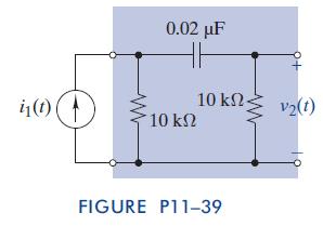
The circuit in Figure P11–39 is in the steady state with i1(t) ¼ 10 cos 5000t mA.(a) Find the steady-state voltage v2SS(t). Repeat for i1(t) ¼ 5 cos 2500t mA.(b) Verify your answer using OrCAD (see Problem 11–38 for help on OrCAD setup.) i(t) 0.02 F 10 10 v2(t) FIGURE P11-39
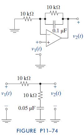
It is claimed that both circuits in Figure P11–74 realize the transfer function TVðsÞ ¼ K s þ 2000 s þ 1000(a) Verify that both circuits realize the specified TV(s).(b) Which circuit would you choose if the output must drive a 1 kV load?(c) Which circuit would you choose if the input comes
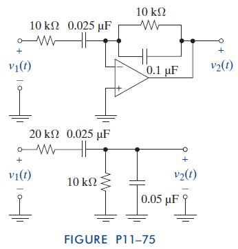
It is claimed that both circuits in Figure P11–75 realize the transfer function TVðsÞ ¼1000sðs þ 1000Þðs þ 4000Þ(a) Verify that both circuits realize the specified TV(s).(b) Which circuit would you choose if the output must drive a 1 kV load?(c) Which circuit would you choose if the
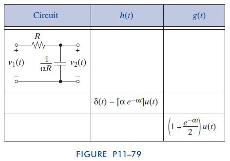
First-Order Circuit Impulse and Step Responses , Each row in the table shown in Figure P11–79 refers to a first-order circuit with an impulse response h(t) and a step response g(t). Fill in the missing entries in the table. Circuit R ww v1(t) R + = v2(t) h(t) g(t) 8(t) - [e-a]u(t) FIGURE P11-79
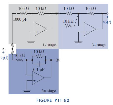
OP AMP Modules and Loading Figure P11–80 shows an interconnection of three basic OP AMP modules.(a) Does this interconnection involve loading?(b) Find the overall transfer function of the interconnection and locate its poles and zeros.(c) Find the steady-state output v2(t) when the input is v1(t)
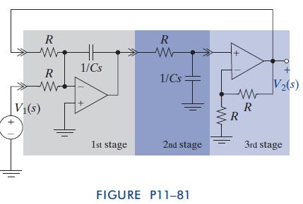
OP AMP Modules and Stability Figure P11–81 shows an interconnection of three basic circuit modules. Does this interconnection involve loading?Find the overall transfer function of the interconnection and locate its poles and zeros. Is the circuit stable? R R ww w 1/Cs R 1/Cs ww + + V(s) ww R R
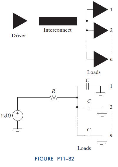
Step Response and Fan-Out The fan-out of a digital device is defined as the maximum number of inputs to similar devices that can be reliably driven by the device output. Figure P11–82 is a simplifieddiagram of a device’s output driving n identical capacitive inputs. To operate reliably, a 5-V
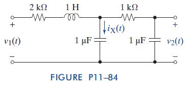
Comparison of Sinusoidal Steady-State Analysis versus Phasor Analysis A circuit designer often is faced with deciding which analysis technique to use when attempting to solve a circuit problem. In this problem we will look at the circuit in Figure P11–84 and choose which technique is the better
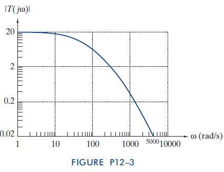
A certain low-pass filter has the Bode diagram shown in Figure P12–3.(a) How many dB down is the filter at 5000 rad/s?(b) Estimate where the cutoff frequency occurs, then determine how many dB down is the filter at one decade after the cutoff frequency? 70 0.2 0.02 IT(joo)| 20 2 w (rad/s) 1 10
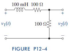
Find the transfer function TV(s) ¼ V2(s)/V1(s) of the circuit in Figure P12–4.(a) Find the dc gain, infinite frequency gain, and cutoff frequency. Identify the type of gain response.(b) Sketch the straight-line approximations of the gain and phase responses.(c) Calculate the gain at v ¼ 0.5vC,
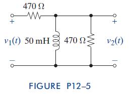
Find the transfer function TV(s) ¼ V2(s)/V1(s) of the circuit in Figure P12–5.(a) Find the dc gain, infinite frequency gain, and cutoff frequency. Identify the type of gain response.(b) Sketch the straight-line approximation of the gain response.(c) Calculate the gain at v ¼ 0.5vC, vC, and
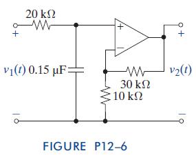
Find the transfer function TV(s) ¼ V2(s)/V1(s) of the circuit in Figure P12–6.(a) Find the dc gain, infinite frequency gain, and cutoff frequency. Identify the type of gain response.(b) Sketch the straight-line approximation of the gain response.(c) Calculate the gain at v ¼ 0.l vC, vC, and
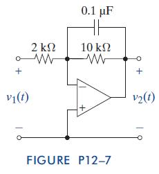
Find the transfer function TV(s) ¼ V2(s)/V1(s) of the circuit in Figure P12–7.(a) Find the dc gain, infinite frequency gain, and cutoff frequency. Identify the type of gain response.(b) Sketch the straight-line approximation of the gain response.(c) Calculate the gain at v ¼ 0.1vC, vC, and
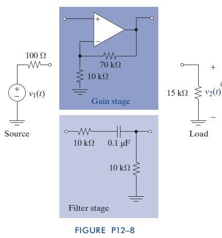
You task is to connect the modules in Figure P12–8 so that the gain of the transfer function is 4 and the cutoff frequency of the filter is 500 rad/s when connected between the source and the load. Repeat if the cutoff frequency is 625 rad/s and the gain did not matter. 100 ww v1(t) Source ww 70
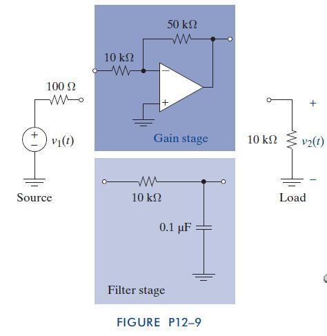
A young designer needed to design a low-pass filter with a cutoff of 1 krad/s and a gain of 5. The filter is to fit as an interface between the source and the load. The designer was perplexed when no matter how the stages shown in Figure P12–9 are connected the results are not what were expected.
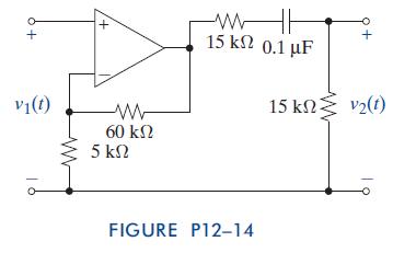
Find the transfer function TV(s) ¼ V2(s)/V1(s) of the circuit in Figure P12–14.(a) Find the dc gain, infinite frequency gain, and cutoff frequency. Identify the type of gain response.(b) Use OrCAD to plot the Bode magnitude gain response of the circuit.(c) What element value would you change to
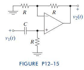
Find the transfer function TV(s) ¼ V2(s)/V1(s) of the circuit in Figure P12–15.What type of gain response does the circuit have? What is the passband gain? Select practical, standard values of R and C from the inside rear cover so that the cutoff frequency is 300 kHz 5%. -o+ v1(t) w R C + FIGURE
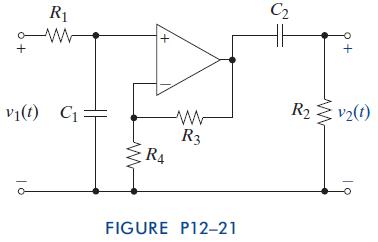
The circuit in Figure P12–21 produces a bandpass response for a suitable choice of element values. Identify the elements that control the two cutoff frequencies. Select the element values so that the passband gain is 100 and the cutoff frequencies are 1000 rad/s and 40 krad/s. Use practical
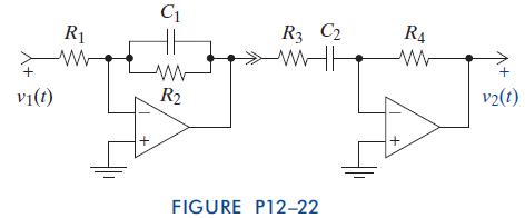
Repeat Problem 12–21 for the circuit in Figure P12–22. Use OrCAD to validate your design. + v1(t) R1 ww C R2 R3 C2 R4 v2(t) + FIGURE P12-22
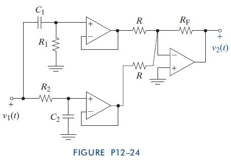
The circuit in Figure P12–24 produces a bandstop response for a suitable choice of element values.(a) Find the circuit’s transfer function.(b) Identify the elements that control the two cutoff frequencies.Select the element values so that the cutoff frequencies are 200 krad/s and 4000 krad/s.
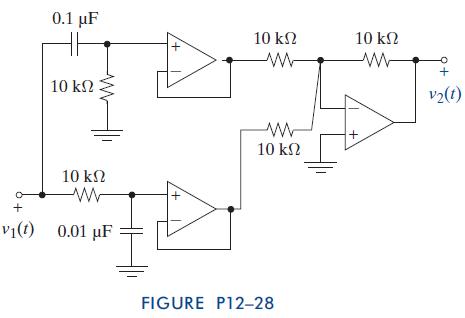
A student needed to design a bandstop filter that was to block frequencies between 1000 rad/s and 10000 rad/s with unity gain in the passbands. His design is shown in Figure P12–28. As a teaching assistant, you are required to grade his design. What grade would you assign and what critique would
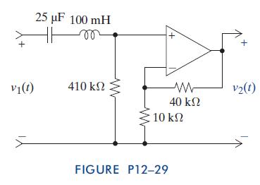
Determine the filter type for the circuit in Figure P12–29.Then find Q, B,vC1,vC2, and v0. Is the circuit a narrow-band or a wide-band filter? + 25 F 100 mH m v1(t) 410 + + www 40 10 v2(t) FIGURE P12-29
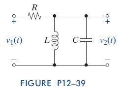
Find the transfer function TV(s) ¼ V2(s)/V1(s) for the bandpass circuit in Figure P12–39. Use MATLAB to visualize the Bode characteristics if R ¼ 50V, L = 500mH, and C =0.002mF. Design an active circuit to meet those characteristics.Verify your design using OrCAD. R ww v1(t) L v2(t) FIGURE
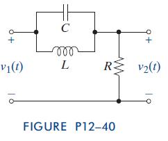
Show that the transfer function TV(s) ¼ V2(s)=V1(s)of the circuit in Figure P12–40 has a bandstop filter characteristic.Derive expressions relating the notch frequency and the cutoff frequencies to R, L, and C. Then select values of R, L, and C so that the bandwidth and the center frequency are
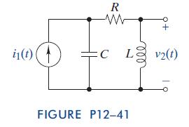
Figure P12–41 shows an RLC filter with an input current and an output voltage. The purpose of this problem is to determine the filter type using informal circuit analysis. Use the element impedances and basic analysis tools to find the magnitude of the output voltage jV2(jv)jat v ¼ 0, v¼1, and
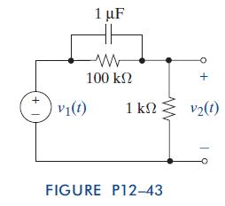
Find the transfer function TV(s) ¼ V2(s)/V1(s) for the circuit in Figure P12–43.(a) Construct the straight-line Bode plot of the gain and phase of the transfer function. Use the straight-line plots to estimate the amplitude and phase of the steady-state output for v1(t) ¼ 10 sin 100t V.(b)
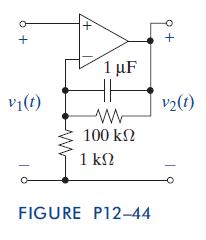
Repeat Prob. 12–43 using the circuit in Figure P12–44. + v1(t) 1 F ww 100 1 + V2(t) FIGURE P12-44
For the following transfer function(a) Construct the straight-line Bode plot of the gain. Is this a low-pass, high-pass, bandpass, or bandstop function? Estimate the cutoff frequency and passband gain.(b) Use MATLAB to plot the Bode magnitude of the transfer function.(c) Design a circuit using
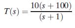
Consider the gain plot in Figure P12–52.(a) Find the transfer function corresponding to the straightline gain plot.(b) Use MATLAB to plot the Bode magnitude of the transfer function.(c) Compare the straight-line gain and the actual gain at v ¼20 and 200 rad/s.(d) Design a circuit to realize the
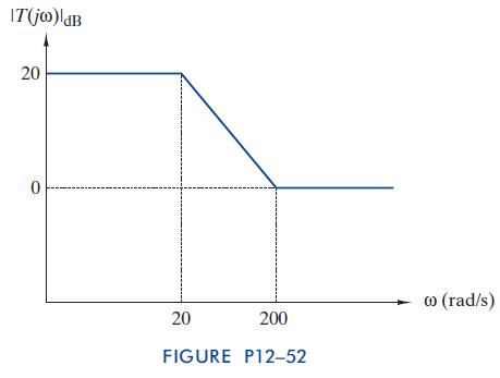
Consider the gain plot in Figure P12–53.(a) Find the transfer function corresponding to the straightline gain plot.(b) Use MATLAB to plot the Bode magnitude of the transfer function.(c) Compare the straight-line gain and the actual gain at v ¼100 and 500 rad/s.(d) Design a circuit that will
Showing 4600 - 4700
of 7343
First
40
41
42
43
44
45
46
47
48
49
50
51
52
53
54
Last
Step by Step Answers