New Semester
Started
Get
50% OFF
Study Help!
--h --m --s
Claim Now
Question Answers
Textbooks
Find textbooks, questions and answers
Oops, something went wrong!
Change your search query and then try again
S
Books
FREE
Study Help
Expert Questions
Accounting
General Management
Mathematics
Finance
Organizational Behaviour
Law
Physics
Operating System
Management Leadership
Sociology
Programming
Marketing
Database
Computer Network
Economics
Textbooks Solutions
Accounting
Managerial Accounting
Management Leadership
Cost Accounting
Statistics
Business Law
Corporate Finance
Finance
Economics
Auditing
Tutors
Online Tutors
Find a Tutor
Hire a Tutor
Become a Tutor
AI Tutor
AI Study Planner
NEW
Sell Books
Search
Search
Sign In
Register
study help
business
systems analysis and design
The Analysis And Design Of Linear Circuits 8th Edition Roland E. Thomas, Albert J. Rosa, Gregory J. Toussaint - Solutions
7. Quadratic nonresidues modulo n The set Q, of quadratic residues modulo n con-sists of those [a], ∈ Z for which we can solve x2 = a mod n for some x with [x], ∈Z(a) Let p be an odd prime and g a primitive root for Z(i) Show that [a], is a quadratic residue modulo p if and only if$$a = g^{2i}
8. **Primality test based on quadratic residues** Assume that there is an efficient algo-rithm Jacobi (a, n) that outputs• 0 if gcd(a, n) > 1,• 1 if a ∈ Qn, and• -1 otherwise(such an algorithm does exist). Assume further that the output of Jacobi (a, n) is equal to a(n - 1)/2 mod n whenever
1. Use your implementation of Miller-Rabin (n,s) to build a user interface that takes as input two natural numbers d; and dy with dd, and produces as very likely out- put a prime number n whose number d of decimal digits satisfies ddd.
2. Show that 232 +1 is not a prime number. (Hint: Since the algorithm Miller- Rabin (n,s) is correct for negative replies, you could use that algorithm for such a "proof".)
3. Run Miller-Rabin (2**16+1,s) for a number of different s. Although it is known that 216 +1 is prime, what is the best probabilistic bound you have for that fact based on your program executions?
4. For a sequence (x)en of real numbers, lim x, exists and equals the real num- ber x if and only if, for all real positive numbers &, there exists some n(E) EN such that the absolute value of x-x, is less than & for all nn(). (a) Prove that lim 1/n = 0. (b) Prove that limits are unique, provided
5. (a) Use Theorem 2.53 to approximate the number of primes whose binary represen- tation has between 512 and 1024 bits. (b) Assume that there are about 1077 atoms in our universe and that this universe is about 100 years old. Assume also that, from the beginning of time, every atom in the universe
6. Sophie Germaine primes A prime number p > 2 is called a Sophie Germaine prime if 2 p+1 is also prime. A 32-bit Sophie Germaine prime is p = 2008465313 with prime 2 p +1 = 4016930627 (found after 644 trials). It took 2253 trials to generate a 64-bit Sophie Germaine prime p = 10155921358726090901
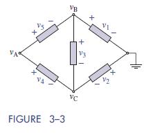
The reference node and node voltages in the bridge circuit of Figure 3–3 are υA =5V,υB = 10 V, and υC = −3 V. Find the element voltages VB V3 VA VA FIGURE 3-3 VC
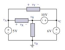
For the circuit in Figure 3–4, first find the node voltages and then find υX and υY. VA + vx +5V +1 + vy VB VD 10V 1+ VC 6V +
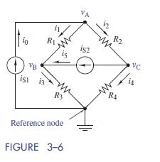
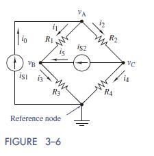
Formulate node-voltage equations for the bridge circuit in Figure 3–6. 40 isi VB R iz is R3 VA is2 (f) R ww RA VC Reference node FIGURE 3-6
For the circuit in Figure 3–6 replace the current source iS2 with a resistor R5.(a) Using the same node designations and reference node, formulate node-voltage equations for the modified circuit. Place the result in matrix form Ax= b.(b) Is the resulting A matrix symmetrical? VB isl R is iz R3 VA
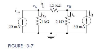
Formulate node-voltage equations for the circuit in Figure 3–7 and place the results in matrix form Ax=b. Is the resulting matrix A symmetrical? 1.5 VB w Ais 114 Stiz 20 mA FIGURE 3-7 -1 k 50 mA
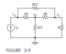
Formulate node-voltage equations for the circuit in Figure 3–9. R/2 ww 2R 2R VA VB VC www ww is R/2 FIGURE 3-9
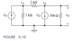
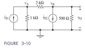
Formulate node-voltage equations for the circuit in Figure 3–10 VA FIGURE 3-10 2 VB www + 1 kQ is20 500
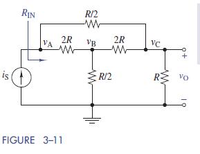
Given the circuit in Figure 3–11, find the input resistance RIN seen by the current source and the output voltage υO. Solve this problem by hand and then using MATLAB. RIN R/2 www 2R 2R VA VB VC ww w R/2 R VO FIGURE 3-11
Solve the node-voltage equations in Exercise 3–5 for υO in Figure 3–10. VA FIGURE 3-10 2 www VB isz 1 kQ is20 + 500
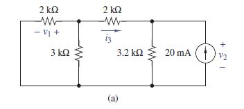
Use node-voltage equations to solve for υ1, υ2, and i3 in Figure 3–12(a). 2 ww - V + 3 www 2 ww 3.2 20 mA V2 (a)
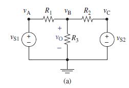
Use node-voltage analysis to find υO in the circuit in Figure 3–14(a). VSI VA +1 R VB ww R VC ww + VOR3 1 + VS2
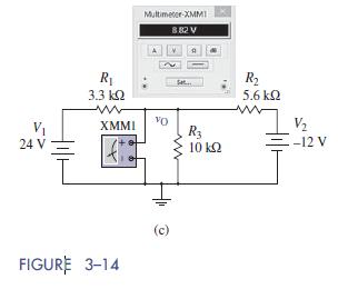
In Figure 3–14(a), υS1 =24V, υS2 = −12 V, R1 =3:3 kΩ, R2 =5:6 kΩ, and R3 =10 kΩ. Find υO using Multisim. 24 V R 3.3 w Multimeter-XMMI 882 V R 5.6 vo XMMI V R3 -12 V 10 FIGURE 3-14 (c)
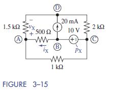
Use node-voltage analysis to find υX in the circuit of Figure 3–15. 20 mA 1.5 2 1500 10 V (A) www (+1) B Px www FIGURE 3-15
For the circuit of Figure 3–15, find iX and pX. 20 mA 1.5 2 1500 10 V www (+1) B Px www FIGURE 3-15
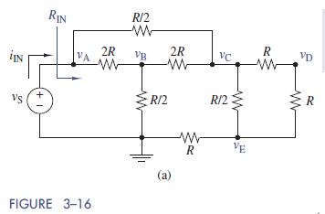
Find the input resistance of the circuit in Figure 3–16(a). Solve the problem using MATLAB. RIN R/2 ww 2R 2R R IN VA VB VC VD ww w www + w R/2 R/2 R w R VE (a) FIGURE 3-16
For the circuit in Figure 3–16(a) let υS = 120 V and R=4 kΩ.(a) Use Multisim to simulate the circuit, and find all of the node voltages and the input current.(b) Verify that the results for the node voltages agree with the numeric expressions determined in the solution of Example 3–6.(c) Use
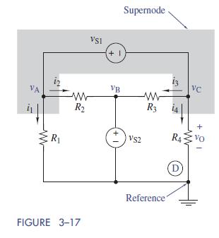
For the circuit in Figure 3–17,(a) Formulate node-voltage equations.(b) Solve for the output voltage υO using R1 =R4 =2 kΩ and R2 =R3 =4 kΩ. Supernode VSI +1 VC VB ww VA ww 12 R ww R +1 R3 +1 ww R4 VS2 D FIGURE 3-17 Reference
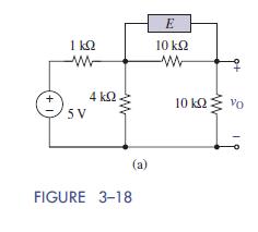
For the circuit in Figure 3–18(a),(a) Find υO when element E is a 10-kΩ resistor.(b) Find υO when element E is a 4-mA independent current source with reference arrow pointing left.(c) If element E is a resistor R, what value is required for R such that υO is 2 V? ww E 10 ww +1 5V 4 . 10 Vo
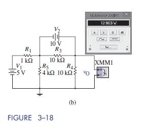
For the circuit in Figure 3–18(a),(a) Find υO when element E is an open circuit.(b) Find υO when element E is a 10-V independent voltage source with the positive reference on the right.(c) Validate part (b) using Multisim. R www V 10 V R3 w Mulator XMM 12 963 W 10 XMMI V E5V R5 RA 4 10
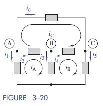
In Figure 3–20 the mesh currents are iA =10A, iB = 5 A, and iC = −3A. Find the element currents i1 through i6 and show that KCL is satisfied at nodes A, B, and C. i6 A) ic 13 FIGURE 3-20 B C is iB
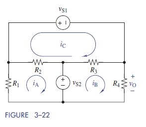
For the circuit of Figure 3–22,(a) Formulate mesh-current equations.(b) Find the output υO using R1 =R4 =2 kΩ and R2 =R3 =4 kΩ using MATLAB VSI +1 R www R iA ic +- w R3 + VS2 iB RAVO ww FIGURE 3-22
Using the circuit of Figure 3–18 (see Exercises 3–12 and 3–13), use mesh-current analysis to find the current through the 4-kΩ resistor and the voltage υO when the element E is(a) a 10-kΩ resistor.(b) a 10-V independent voltage source with the positive reference on the right.
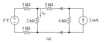
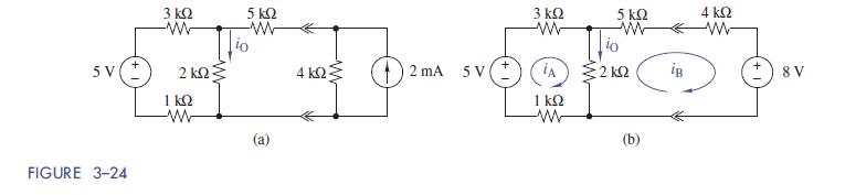
Use mesh-current equations to find iO in the circuit in Figure 3–24(a). 5V(+ 3 www 2 1 ww 5 ww (a) 4 ww 2 mA
In Figure 3–24 replace the 5-V source with a 1-mA dc current source with the arrow pointing up. Use source transformations to reduce the circuit to a single mesh and then solve for iO. 3 - 5 - 5V 2 4 +2 mA 5V FIGURE 3-24 ww (a) 3 ww 5 4 www www io 1 www (b) 8V
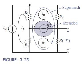
Use mesh-current equations to find υO in Figure 3–25. ww iB S2 R Supermesh Excluded w R3 FIGURE 3-25 R4 VO
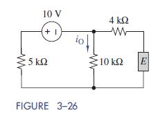
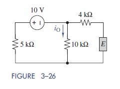
Use mesh analysis to find the current iO in Figure 3–26 when the element E is(a) a 5-V voltage source with the positive reference at the top.(b) a 10-kΩ resistor. 10 V +1 - 5 4 www io 10 E FIGURE 3-26
Use mesh analysis to find the current iO in Figure 3–26 when the element E is(a) A 1-mA current source with the reference arrow directed down(b) Two 20-kΩ resistors in parallel 10 V +1 - 5 4 www io 10 E FIGURE 3-26
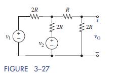
Write a set of mesh-current equations for the circuit in Figure 3–27. Do not solve the equations. 2R R V FIGURE 3-27 1+ 2R 2R Vo
Use mesh-current equations to find υO in Figure 3–27 2R R ww 2R 2R Vo V +1) FIGURE 3-27
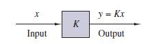
Refer to the block diagram shown in Figure 3–28.(a) A certain linear device has a K of 0:35. Its output is 6 V. What is the input that will produce that output?(b) A different linear device outputs 910mA when its input is 1A. What will be its output when the input to the device is 300 mA? X Input
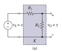
Suppose the voltage divider shown in Figure 3–29(a) has a K of 0.75. How would one go about changing the K so that it will have a K of 0:8? Vs= R ww R Vo=y +1 K (a)
Design a circuit that has a K = υO=υS =0:67 using standard value resistors. (See inside back cover.)
Design a circuit that has K = iO=iS =0:9 using 5% tolerance standard value resistors. (See inside back cover
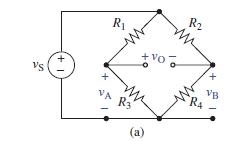
You are given the bridge circuit of Figure 3–30(a).(a) Find the proportionality constant K in the input-output relationship υO =KυS.(b) Find the sign of K when R2R3 >R1R4, R2R3 =R1R4, and R2R3 (c) Draw a block diagram of this relationship VS +- R + VA R3 +vo R + VB (a) R4
In Figure 3–30(a) select values of R so that K = −0:333. +1 + VB + R VA R3 (a) vo R R4
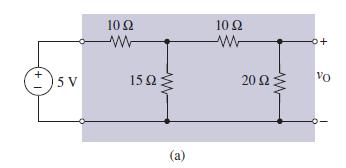
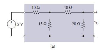
Use the unit output method to find υO in the circuit shown in Figure 3–31(a). 10 10 ww w ++ + 5 V 15 ww 20 VO (a)
Find υO in the circuit of Figure 3–31(a) when υS is −5 V, 10 mV, and 3 kV. 10 ww 10 w 0+ + 5 V 15 20 VO (a)
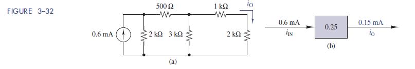
For the circuit in Figure 3–32(a),(a) Use the unit output method to find K = iO=iIN(b) Then use the proportionality constant K to find iO for the input current shown in the figure.(c) Draw a block diagram to show the results of parts (a) and (b). FIGURE 3-32 0.6 mA 500 ww 3 1 ww (a) 0.6 mA
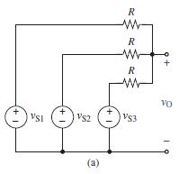
Figure 3–37(a) shows a resistance circuit used to implement a signal-summing function.Use superposition to show that the output υO is a weighted sum of the inputs υS1,υS2, and υS3. +1 VSI + VS2 (a) 1+ R ww R ww R VS3 + VO
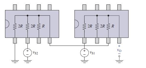
The circuit of Figure 3–38 contains two R-2R modules. Use superposition to find υO. 2R 2R R H VS2 ww 2R 2R R VSI ii 1+010||||1
Repeat Exercise 3–27 with the voltage source υS2 replaced by a current source iS2 with the current reference arrow directed toward ground.
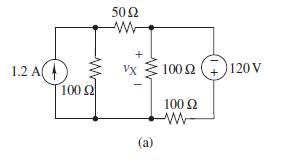
Use the principle of superposition to find the voltage υX in Figure 3–39(a). Validate your answer using Multisim. 1.2 A 100 50 ww (a) 100 2120 V 100 ww
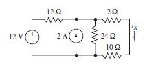
Use the principle of superposition to find the current iX in Figure 3–40. 120 ww 202 ww ix 12 V 2A 24 100 www
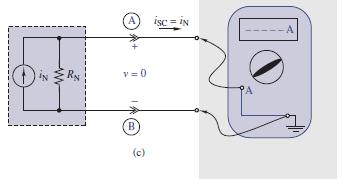
Thévenin measurements can be made in the laboratory or in the field with a simple digital multimeter (DMM). Look at Figure 3–43(c). If one sets the DMM to read voltage, then the multimeter acts like an open circuit1 and the meter reading will be the circuit’s open-circuit voltage υOC. Setting
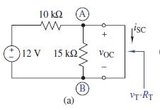
Find the Thévenin equivalent at nodes A and B for the circuit in Figure 3–45(a). +1 10 ww 12 V 15 k2) (A) + VOC (a) B isc VT RT
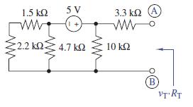
Find the Thévenin equivalent at nodes A and B for the circuit in Figure 3–46. 1.5 www 5 V 12.2 4.7 3.3 www 10 B VT RT
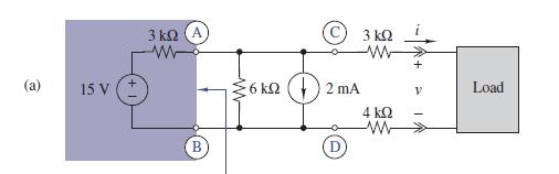
(a) Find the Thévenin equivalent circuit of the source circuit to the left of the interface in Figure 3–47(a).(b) Use the Thévenin equivalent to find the power delivered to two different loads. The first load is a 10-kΩ resistor and the second is a 5-V voltage source whose positive terminal is
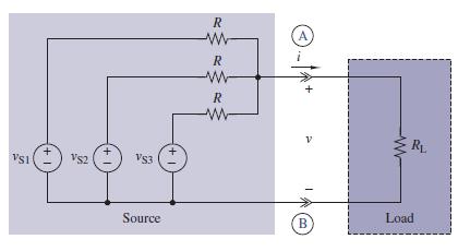
(a) Find the Thévenin equivalent of the source circuit to the left of the interface in Figure 3–52(a).(b) Use the Thévenin equivalent to find the voltage delivered to the load VSI 1+ VS2 1+ VS3 1+ R ww R ww R www Source B -12+ V R Load
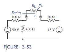
For the circuit of Figure 3–53 find the Thévenin equivalent circuit seen by RL. Then use the equivalent circuit to find the load power pL when RL =50 Ω, 100 Ω, and 500 Ω. RT VT 100 RL PL 20 +1 50 V +- 400 15 V ( F|GURE 3-53
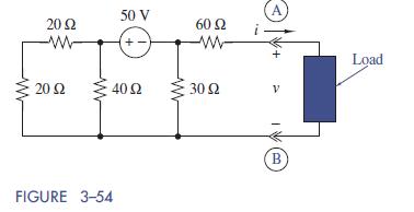
(a) Find the Thévenin and Norton equivalent circuits seen by the load in Figure 3–54.(b) Find the voltage, current, and power delivered to a 50-Ω load resistor 20 ww 50 V + 60 w A 20 40 30 FIGURE 3-54 A B IVA Load
Find the current and power delivered to an unknown load in Figure 3–54 when υ= +6V. 20 w 50 V + 60 w A 20 40 30 FIGURE 3-54 A IVA B Load
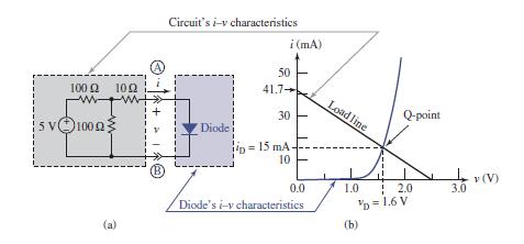
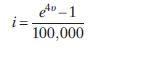
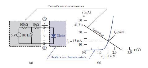
Find the voltage, current, and power delivered to the diode in Figure 3–56(a). The diode’s i–v characterististics are given in Figure 3–56(b).Suppose for the circuit shown in Figure 3–56(a) that the diode’s i−υ characteristics can be modeled by the following equationwhere υ is given
A source circuit with υT =2:5 V and RT =60 Ω drives a load with RL =30 Ω.(a) Determine the maximum signal levels available from the source circuit.(b) Determine the actual signal levels delivered to the load
A source circuit delivers 4 V when a 50-Ω resistor is connected across its output and 5 V when a 75-Ω resistor is connected. Find the maximum voltage, current, and power available from the source.
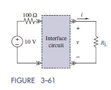
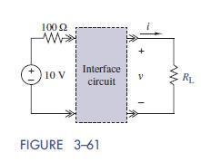
Select the load resistance in Figure 3–61 so that the interface signals are in the range defined by υ ≥ 4 V and i ≥ 30 mA. 1002 _ 10 V Interface circuit RL FIGURE 3-61
Select RL in Figure 3–61 so that 19010%mWare delivered to the load. Select a 10% resistor from inside the back cover that will provide the desired power. 100 Q ............ 10.V Interface RL circuit FIGURE 3-61
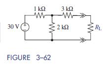
Select a 5% standard-value load resistor RL for the circuit in Figure 3–62 that will result in 10 V5% delivered across it 30 V ( w 3 w 2 ko W FIGURE 3-62 RL
For the circuit of Figure 3–62, select a load resistor, if possible, so that 6mAflows through it. 30 V 1 w 3 M-> 2 FIGURE 3-62 RL
For the circuit of Figure 3–62, determine the maximum power available, and if sufficient, select a resistive load that will dissipate 20 mW. 30 V 1 w 3 ww 2 FIGURE 3-62 RL
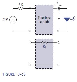
Suppose the source circuit in Figure 3–63 is now 12 V in series with a 5-Ω source resistor.The same LED is used. How does the solution change 5V 202 w Interface circuit FIGURE 3-63 ww R
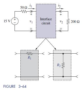
Design two versions of the interface circuit in Figure 3–64 that deliver υ2 = 5 V to the 200-Ω load. Evaluate the two designs in terms of power loss in the interface circuit 15 V FIGURE 3-64 1+ 50 VI Interface circuit V2 200 ww R R
ANorton source of 300mAin parallel with a 50-Ω source resistor provides current to a load RL = 200 Ω. Your task is to design an interface so that 5 V10% are delivered to the load.(a) Using the series resistor RS interface shown in Figure 3–59(b), select a 10% resistor from the inside back cover
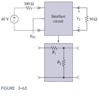
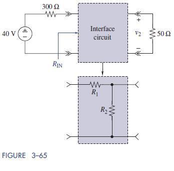
Design the interface circuit in Figure 3–65 so that the 40-V source delivers υ2 =2Vto the output load and the resistance seen at the input port is RIN = 300 Ω. Note that this means that the input resistance of the two ports matches the source resistance 40 V (+ 300 www Interface V2 502 circuit
Repeat Example 3–27 with the desired υ2 = 10 V instead of 2 V.
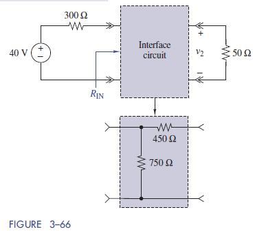
In Example 3–27 we designed the interface circuit in Figure 3–65 to meet the requirementsυ2 = 2 V and RIN = 300 Ω. It is claimed that the interface circuit in Figure 3–66 meets the same requirements.(a) Verify that the circuit in Figure 3–66 produces υ2 = 2 V and RIN = 300 Ω.(b) It is
Use Multisim to determine which solution, Figure 3–65 or Figure 3–66, requires less power from the source. 40 V (+ 300 ww FIGURE 3-66 Interface circuit RIN w 450 750 V2 www : 50
Design the interface circuit in Figure 3–67 so the 50-Ω load “sees” a Thévenin resistance of 50 Ω between terminals C and D, while simultaneously the input voltage source “sees” an input resistance of 300 Ω between terminalsAand B. Meeting these two constraints produces matched
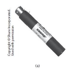
A common problem is interfacing a TV antenna’s 300-Ω line to a 75-Ω cable input on an HDTV set. Repeat Example 3–29 for this particular interface. See Figure 3–68 for a photo of such a device. www.ShowMeCables.com
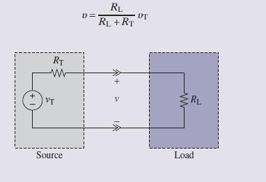
The source-load interface in Figure 3–69 serves to introduce an important concept that we will encounter many times in subsequent chapters. By simple voltage division, the interface voltage is +1 RT www VT 1)= RL RL+RT DT RL Source Load
SupposeRT = 200 Ωand the loading effect should be less than 1%. What should be the smallest value for RL?
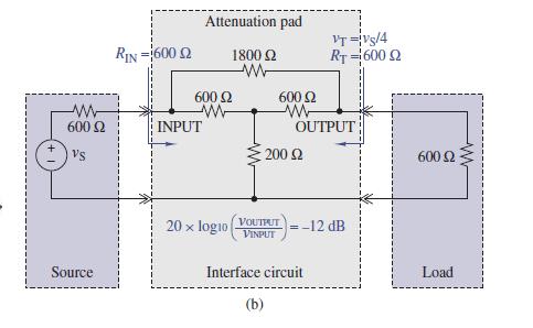
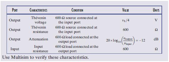
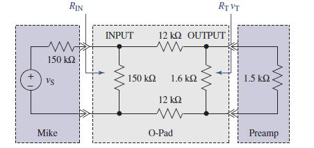
An attenuation pad is a two-port resistance circuit that provides a nonadjustable reduction in signal level while also providing resistance matching at the input and output ports. Attenuators are used in numerous applications such as in audio recording studios to reduce the signal coming from a
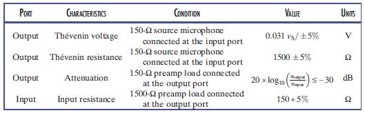
The manufacturer’s data sheet for the following O-pad used to attenuate the signal from a 150-Ω microphone to a 1500-Ω preamp load specifies the following characteristics at the input and output ports:Use Multisim to simulate the schematic provided by the manufacturer shown in Figure 3–72 and
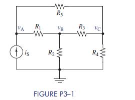
3–1 Formulate node-voltage equations for the circuit in Figure P3−1. Arrange the results in matrix form Ax= b. www Rs R3 R VB VC VA www ww is R ww RA FIGURE P3-1
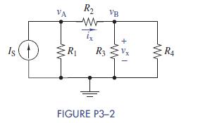
3–2 (a) Formulate node-voltage equations for the circuit in Figure P3−2. Arrange the results in matrix form Ax= b.(b) Solve these equations for vA and vB.(c) Use these results to find vx and ix. Is VA ww R R www T R3 VB w FIGURE P3-2 ww R4
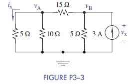
3–3 (a) Formulate node-voltage equations for the circuit in Figure P3−3. Arrange the results in matrix form Ax= b.(b) Solve these equations for vA and vB.(c) Use these results to find vx and ix. 15 2 VA VB www 352 $100 528 3A 50 50 FIGURE P3-3 + 1
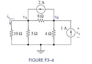
3–4 (a) Formulate node-voltage equations for the circuit in Figure P3−4.(b) Solve these equations for vA and vB.(c) Use these results to find vx and ix. 2 A VA 8 VB www 1 A 100 50 FIGURE P3-4 + Vx
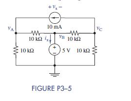
3–5 (a) Formulate node-voltage equations for the circuit in Figure P3−5. Arrange the results in matrix form Ax= b.(b) Solve these equations for vA and vC.(c) Use these results to find vx and ix. +- ww 10 10 10 mA VB www 10 5V 10 kQ VC FIGURE P3-5
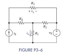
3–6 (a) Choose a ground wisely and formulate node-voltage equations for the circuit in Figure P3−6.(b) Solve for vx and ix when R1 =R2 =R3 =R4 =5 kΩ, vS =12 V, and iS = 2 mA. R4 ww R3 ww +- www ww R R VS FIGURE P3-6 +1
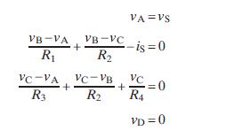
3–7 The following are a set of node-voltage equations; draw the circuit they represent VA VS VB-VA R + VB-VC-is=0 R VC-VA VC-VB R3 + R2 + R4 VD=0
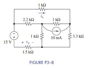
3–8 (a) Choose a ground wisely and formulate node-voltage equations for the circuit in Figure P3−8.(b) Solve for vx and ix.(c) Validate your answers using Multisim. 2.2 ww 1 w 1 ww 15 V + Vx 1 3.3 10 mA ww 1.5 FIGURE P3-8
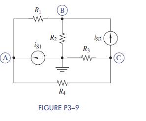
3–9 (a) Formulate node-voltage equations for the circuit in Figure P3−9.(b) Use MATLAB to find symbolic expressions for the node voltages in terms of the parameters in the circuit.(c) Find numeric values for vA, vB, and vC when R1 =1 kΩ, R2 =1:5 kΩ, R3 =2:2 kΩ, R4 =3:3 kΩ, iS1= 1mA, and iS2
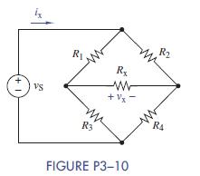
3–10 (a) Formulate node-voltage equations for the bridge circuit in Figure P3−10.(b) Solve for vx and ix when R1 =R4 =1 kΩ,R2 =R3 = 1:5 kΩ, Rx = 680 Ω, and vS =12V.(c) Repeat (b) when R4 is a variable resistor that varies from 10 Ω to 10 kΩ.At what value of R4 is the voltage across Rx = 0
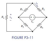
3–11 (a) Formulate node-voltage equations for the circuit in Figure P3−11.(b) Solve for vx and ix when R1 =1 kΩ, R2 =1:5 kΩ, R3 = 500 Ω, R4 =2 kΩ, Rx = 100 Ω, and vS =15V. Rx +1 R R3 + FIGURE P3-11 R Ra
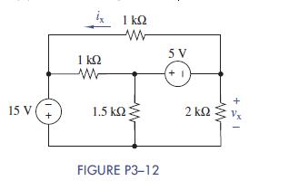
3–12 (a) Formulate node-voltage equations for the circuit in Figure P3−12. (Hint: Use a supernode.)(b) Solve for vx and ix.(c) Verify your results using Multisim. + % w 2 15 V 1 kQ w 1.5 1 kQ ww ww 5 V FIGURE P3-12
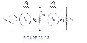
3–13 (a) Formulate mesh-current equations for the circuit in Figure P3−13. Arrange the results in matrix form Ax = b.(b) Solve for iA and iB.(c) Use these results to find vx and ix VS 1 + R ww R3 ww iA R iB R4 FIGURE P3-13
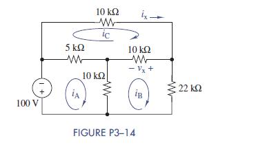
3–14 (a) Formulate mesh-current equations for the circuit in Figure P3−14. Arrange the results in matrix form Ax = b.(b) Solve for iA, iB, and iC.(c) Use these results to find vx and ix. 1+ 100 V 5 www iA 10 w 10 ic ww 10 ww Vx+ iB FIGURE P3-14 22
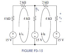
3–15 (a) Formulate mesh-current equations for the circuit in Figure P3−15. Arrange the results in matrix form Ax = b.(b) Solve for iA and iB.(c) Use these results to find vx and ix 4 ww 2 ww 4 2 w 15 V AiA 15 V 4 iB FIGURE P3-15 + + 15 V
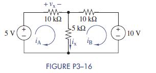
3–16 (a) Formulate mesh-current equations for the circuit in Figure P3−16. Arrange the results in matrix form Ax = b.(b) Solve for iA and iB.(c) Use these results to find vx and ix.(d) Solve this problem using node-voltage equations and compare your answers with the mesh-current approach.Which
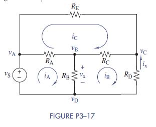
3–17 (a) Formulate mesh-current equations for the circuit in Figure P3−17.(b) Formulate node-voltage equations for the circuit in Figure P3−17.(c) Which set of equations would be easier to solve? Why?(d) Using MATLAB, find vx and ix in terms of the meshcurrent variables.(e) Using MATLAB, find
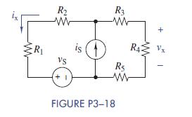
3–18 (a) Formulate mesh-current equations for the circuit in Figure P3−18. (Hint: Use a supermesh.)(b) Solve for vx and ix when R1 =2:7 kΩ, R2 =1:5 kΩ, R3 =680 Ω, R4 =2:2 kΩ, R5 =3:3 kΩ, iS = 10 mA, and vS =12V.(c) Use Multisim to verify your results in part (b) and then find the total
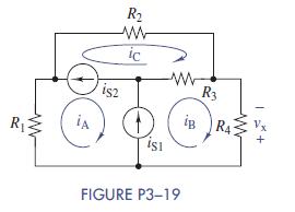
3–19 (a) For the circuit of Figure P3−19 solve for iA, iB, and iC using supermesh principles.(b) Use these results to find vx. R2 w iA is2 R w ic R3 iB RA R4Vx + FIGURE P3-19
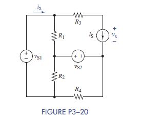
3–20 (a) Formulate mesh-current equations for the circuit in Figure P3−20.(b) Use MATLAB to find symbolic expressions for vx and ix in terms of the parameters in the circuit.(c) Find numeric values for vx and ix when R1 =R2 =8:2 kΩ, R3 =2:2 kΩ,R4 =3:3 kΩ, iS =2:5 mA, vS1 = 15 V, and vS2
Showing 5300 - 5400
of 7343
First
47
48
49
50
51
52
53
54
55
56
57
58
59
60
61
Last
Step by Step Answers