New Semester
Started
Get
50% OFF
Study Help!
--h --m --s
Claim Now
Question Answers
Textbooks
Find textbooks, questions and answers
Oops, something went wrong!
Change your search query and then try again
S
Books
FREE
Study Help
Expert Questions
Accounting
General Management
Mathematics
Finance
Organizational Behaviour
Law
Physics
Operating System
Management Leadership
Sociology
Programming
Marketing
Database
Computer Network
Economics
Textbooks Solutions
Accounting
Managerial Accounting
Management Leadership
Cost Accounting
Statistics
Business Law
Corporate Finance
Finance
Economics
Auditing
Tutors
Online Tutors
Find a Tutor
Hire a Tutor
Become a Tutor
AI Tutor
AI Study Planner
NEW
Sell Books
Search
Search
Sign In
Register
study help
computer science
computer system architecture
Computer System Architecture 3rd Edition M. Morris Mano - Solutions
What is the minimum number of bits that a frame must have in the bit-oriented protocol?
Show how the zero insertion works in the bit-oriented protocol when a zero followed by the 10 bits that represent the binary equivalent of 1023 are transmitted.
a. How many 128 x 8 RAM chips are needed to provide a memory capacity of 2048 bytes? b. How many lines of the address bus must be used to access 2048 bytes of memory? How many of these lines will be common to all chips? c. How many lines must be decoded for chip select? Specify the size of the
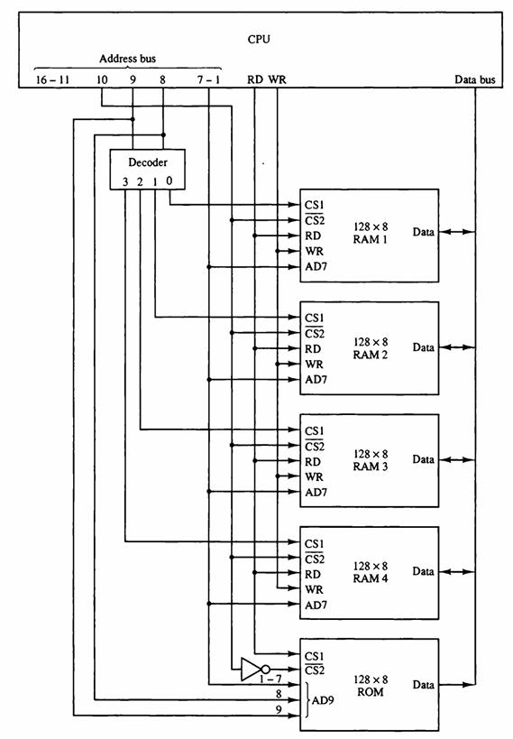
Extend the memory system of Fig. 12-4 to 4096 bytes of RAM and 4096 bytes of ROM. List the memory-address map and indicate what size decoders are needed.Fig. 12-4 16-11 Address bus 10 98 Decoder 3210 7-1 CPU RD
A ROM chip of 1024 x 8 bits has four select inputs and operates from a 5-volt power supply. How many pins are needed for the IC package? Draw a block diagram and label all input and output terminals in the ROM.
A computer employs RAM chips of 256 x 8 and ROM chips of 1024 x 8. The computer system needs 2K bytes of RAM, 4K bytes of ROM, and four interface units, each with four registers. A memory-mapped I/O configuration is used. The two highest-order bits of the address bus are assigned 00 for RAM, 01 for
What is the transfer rate of an eight-track magnetic tape whose speed is 120 inches per second and whose density is 1600 bits per inch?
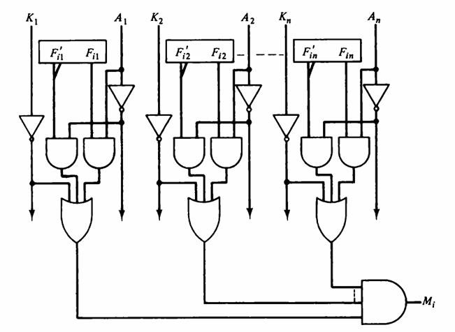
Obtain the complement function for the match logic of one word in an associative memory. In other words, show that M'i is the sum of exclusive-OR functions. Draw the logic diagram for M'i and terminate it with an inverter to obtain Mi.
Obtain the Boolean function for the match logic of one word in an associative memory taking into consideration a tag bit that indicates whether the word is active or inactive.
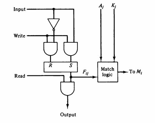
a. Draw the logic diagram of all the cells of one word in an associative memory. Include the read and write logic of Fig. 12-8 and the match logic of Fig. 12-9. Fig. 12-8Fig. 12-9b. Draw the logic diagram of all cells along one vertical column (column j) in an associative memory. Include a common
What additional logic is required to give a no-match result for a word in an associative memory when all key bits are zeros?
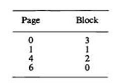
A virtual memory has a page size of 1K words. There are eight pages and four blocks. The associative memory page table contains the following entries:Make a list of all virtual addresses (in decimal) that will cause a page fault if used by the CPU. Page 0 1 4 96 Block 3120
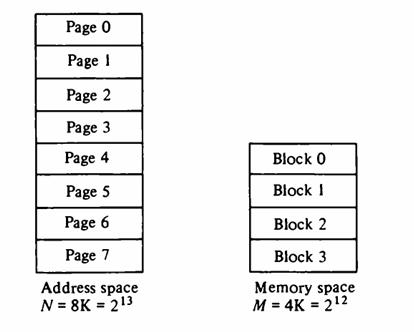
A virtual memory system has an address space of 8K words, a memory space of 4K words, and page and block sizes of 1K words (see Fig. 12-18). The following page reference changes occur during a given time interval. (Only page changes are listed. If the same page is referenced again, it is not listed
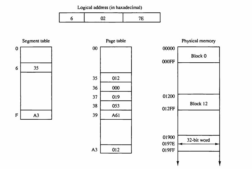
Determine the two logical addresses from Fig. 12-24(a) that will access physical memory at hexadecimal address 012AF.Fig. 12-24(a) 0 6 F Segment table 35 A3 6 Logical address (in haxadecimal) 02 00 35 36 37 38 39 A3 Page
The logical address space in a computer system consists of 128 segments. Each segment can have up to 32 pages of 4K words in each. Physical memory consists of 4K blocks of 4K words in each. Formulate the logical and physical address formats.
Three types of switches are used to design a multistage interconnection network: an interchange switch with two inputs and two outputs as in Fig. 13-6, an arbitration switch with two inputs and one output, and a distribution switch with one input and two outputs. a. Show how the arbitration and
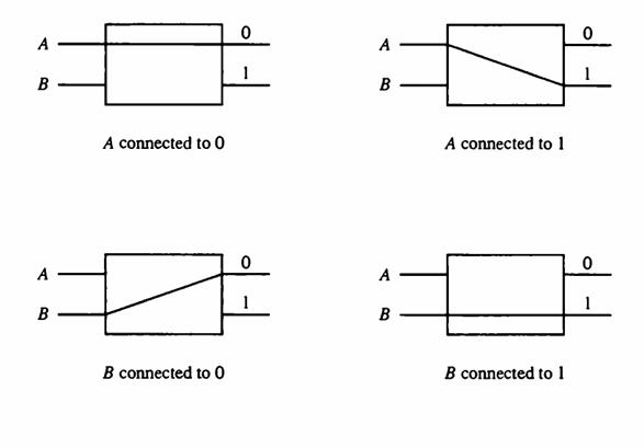
Construct a diagram for a 4 x 4 omega switching network. Show the switch setting required to connect input 3 to output 1.
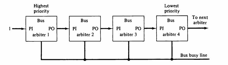
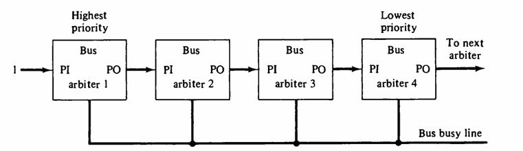
Draw a logic diagram using gates and flip-flops showing the circuit of one bus arbiter stage in the daisy-chain arbitration scheme of Fig. 13-10.Fig. 13-10 PI Highest priority Bus PO arbiter 1 PI Bus PO arbiter 2 PI Bus PO arbiter 3 PI Lowest priority Bus PO arbiter 4 To next arbiter Bus busy line
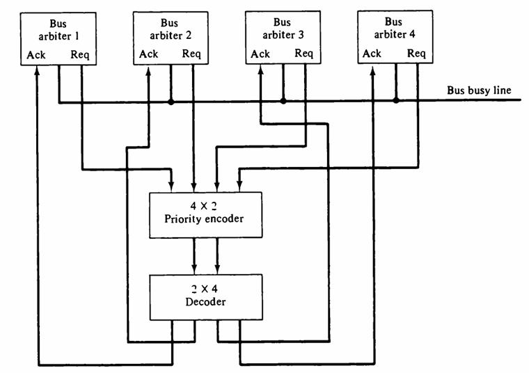
The bus controlled by the parallel arbitration logic shown in Fig. 13-11 is initially idle. Devices 2 and 3 then request the bus at the same time. Specify the input and output binary values in the encoder and decoder and determine which bus arbiter is acknowledged.Fig. 13-11 Bus arbiter 1 Ack
Draw a diagram showing the structure of a four-dimensional hypercube network. List all the paths available from node 7 to node 9 that use the minimum number of intermediate nodes.
Show how the arbitration logic of Fig. 13-10 can be modified to provide a rotating daisy-chain arbitration procedure. Explain how the priority is deter- mined once the bus line is disabled. Fig. 13-10 PI Highest priority Bus PO arbiter 1 PI Bus PO arbiter 2 PI Bus PO arbiter
Consider a bus topology in which two processors communicate through a buffer in shared memory. When one processor wishes to communicate with the other processor it puts the information in the memory buffer and sets a flag. Periodically, the other processor checks the flags to determine if it has
Describe the following terminology associated with multiprocessors. (a) Mutual exclusion; (b) Critical section; (c) Hardware lock; (d) Semaphore; (e) Test-and-set instruction.
What is cache coherence, and why is it important in shared-memory multi-processor systems? How can the problem be resolved with a snoopy cache controller?
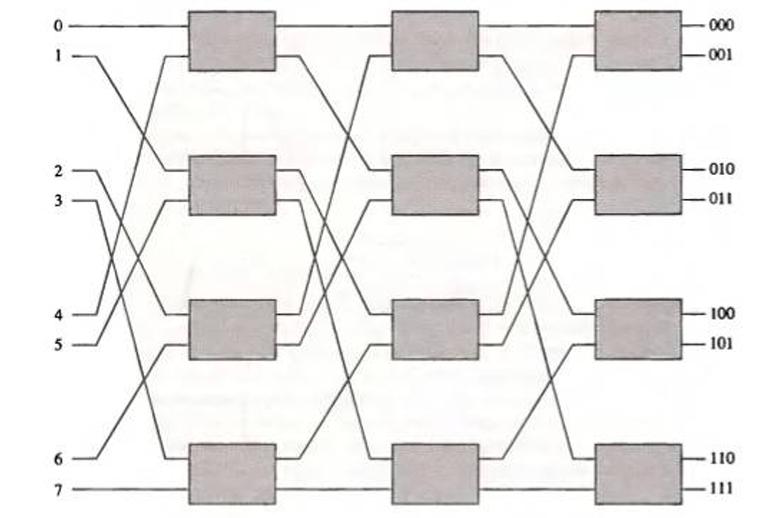
Suppose that the wire breaks between the switch in the first row, second column and the switch in the second row, third column in the omega switching network of Fig. 13-8. What paths will be disconnected?Fig. 13-8 0 2 3 لا 6 7 000 001 -010 -011 100 - 101 110 -111
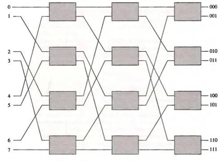
The 8 x 8 omega switching network of Fig. 13-8 has three stages with four switches in each stage, for a total of 12 switches. How many stages and switches per stage are needed in an n x n omega switching network?Fig. 13-8 0 1 23 t 5 6 7 000 -001 8.88 - 010 -011 100 101 110 -111
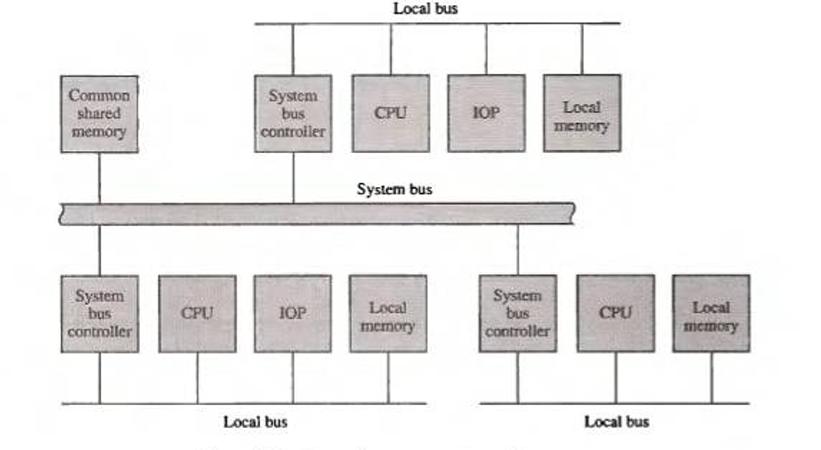
What is the purpose of the system bus controller shown in Fig. 13-2? Explain how the system can be designed to distinguish between references to local memory and references to common shared memory.Fig. 13-2 Common shared memory System bus controller CPU System bus controller IOP Local bus Local
How many switch points are there in a crossbar switch network that connects p processors to m memory modules?
Discuss the difference between tightly coupled multiprocessors and loosely coupled multiprocessors from the viewpoint of hardware organization and programming techniques.
Give the binary number of the logical address formulated in Prob. 12-23 for segment 36 and word number 2000 in page 15.Prob. 12-23The logical address space in a computer system consists of 128 segments. Each segment can have up to 32 pages of 4K words in each. Physical memory consists of 4K blocks
Showing 300 - 400
of 330
1
2
3
4
Step by Step Answers