New Semester
Started
Get
50% OFF
Study Help!
--h --m --s
Claim Now
Question Answers
Textbooks
Find textbooks, questions and answers
Oops, something went wrong!
Change your search query and then try again
S
Books
FREE
Study Help
Expert Questions
Accounting
General Management
Mathematics
Finance
Organizational Behaviour
Law
Physics
Operating System
Management Leadership
Sociology
Programming
Marketing
Database
Computer Network
Economics
Textbooks Solutions
Accounting
Managerial Accounting
Management Leadership
Cost Accounting
Statistics
Business Law
Corporate Finance
Finance
Economics
Auditing
Tutors
Online Tutors
Find a Tutor
Hire a Tutor
Become a Tutor
AI Tutor
AI Study Planner
NEW
Sell Books
Search
Search
Sign In
Register
study help
computer science
computer system architecture
Computer System Architecture 3rd Edition M. Morris Mano - Solutions
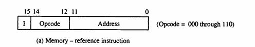
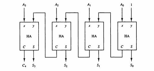
Consider the instruction formats of the basic computer shown in Fig. 5-5 and the list of instructions given in Table 5-2. For each of the following 16-bit instructions, give the equivalent four-digit hexadecimal code and explain in your own words what it is that the instruction is going to
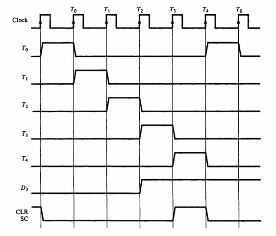
Draw a timing diagram similar to Fig. 5-7 assuming that SC is cleared to 0 at time T3 if control signal C7 is active. C7T3: SC←0 C7 is activated with the positive clock transition associated with T1.Fig. 5-7 Clock To T₁ T₂ 1 T3 TA D3 CLR SC To T₁ T₂ T3 T4 To
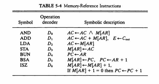
Assume that the first six memory-reference instructions in the basic computer listed in Table 5-4 are to be changed to the instructions specified in the following table. EA is the effective address that resides in AR during time T4. Assume that the adder and logic circuit in Fig. 5-4 can perform
An instruction at address 021 in the basic computer has I = 0, an operation code of the AND instruction, and an address part equal to 083 (all numbers are in hexadecimal). The memory word at address 083 contains the operand B8F2 and the content of AC is A937. Go over the instruction cycle and
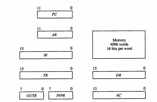
Show the contents in hexadecimal of registers PC, AR, DR, IR, and SC of the basic computer when an ISZ indirect instruction is fetched from memory and executed. The initial content of PC is 7FF. The content of memory at address 7FF is EA9F. The content of memory at address A9F is 0C35. The content
The content of PC in the basic computer is 3AF (all numbers are in hexadecimal). The content of AC is 7EC3. The content of memory at address 3AF is 932E. The content of memory at address 32E is 09AC. The content of memory at address 9AC is 8B9F. a. What is the instruction that will be fetched and
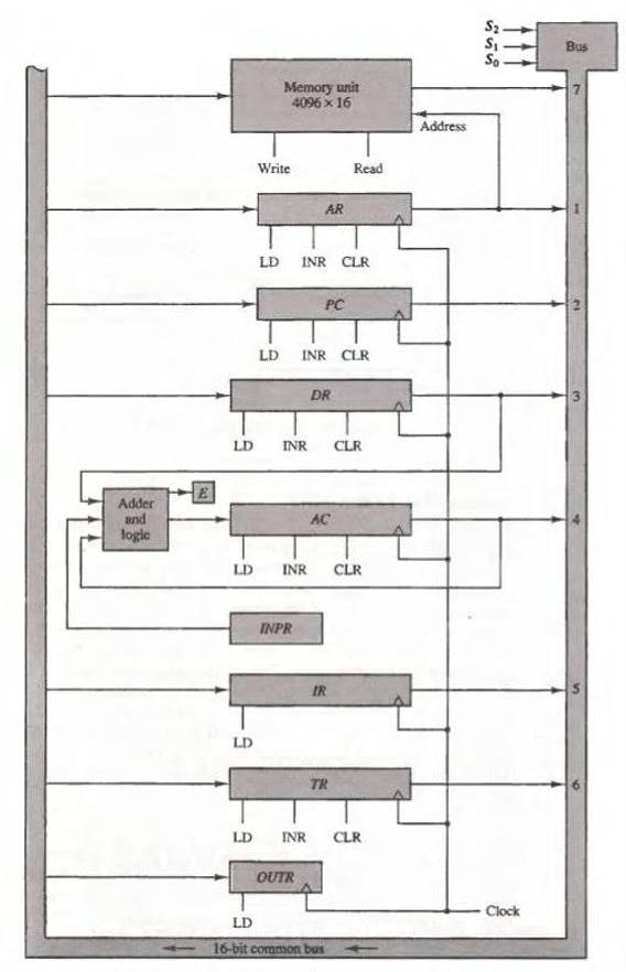
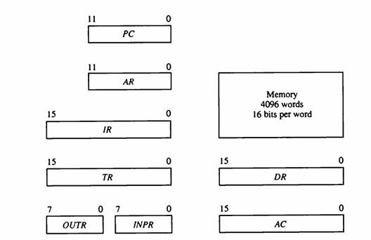
The memory unit of the basic computer shown in Fig. 5-3 is to be changed to a 65,536 x 16 memory, requiring an address of 16 bits. The instruction format of a memory-reference instruction shown in Fig. 5-5(a) remains the same for I = 1 (indirect address) with the address part of the instruction
A computer uses a memory of 65,536 words with eight bits in each word. It has the following registers: PC, AR, TR (16 bits each), and AC, DR, IR (eight bits each). A memory-reference instruction consists of three words: an 8-bit operation-code (one word) and a 16-bit address (in the next two
The register transfer statements for a register R and the memory in a computer are as follows (the X's are control functions that occur at random):X'3X1: R←M[AR] Read memory word into RX'1X2: R←AC Transfer AC to RX'1X3: M[AR]←R
A digital computer has a memory unit with a capacity of 16,384 words, 40 bits per word. The instruction code format consists of six bits for the operation part and 14 bits for the address part (no indirect mode bit). Two instructions are packed in one memory word, and a 40-bit instruction register
An output program resides in memory starting from address 2300. It is executed after the computer recognizes an interrupt when FGO becomes a 1 (while IEN = 1). a. What instruction must be placed at address 1? b. What must be the last two instructions of the output program?
The operations to be performed with a flip-flop F (not used in the basic computer) are specified by the following register transfer statements:xT3: F←1 Set F to 1yT1: F←0 Clear F to 0zT2: F←F Complement FwT5: F←G Transfer value of G
Derive the control gates associated with the program counter PC in the basic computer.
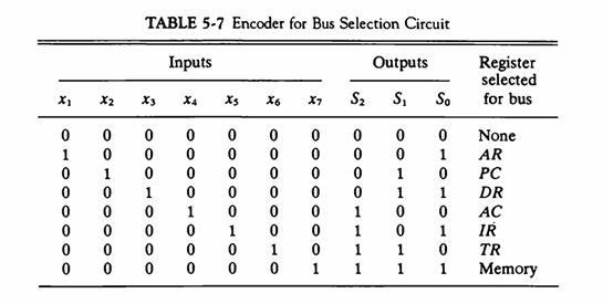
Derive the Boolean logic expression for x (see Table 5-7). Show that x2 can be generated with one AND gate and one OR gate.Table 5-7 0 1 0 0 0 00000000 TABLE 5-7 Encoder for Bus Selection Circuit X2 X3 X4 1 Inputs 00000000 0 1000OOOO 0 X3 X6 OOO OOLOO 0 0 0 0 0 1 2 0 00000000 0 1 Outputs X7 S₂
Derive the control gates for the write input of the memory in the basic computer.
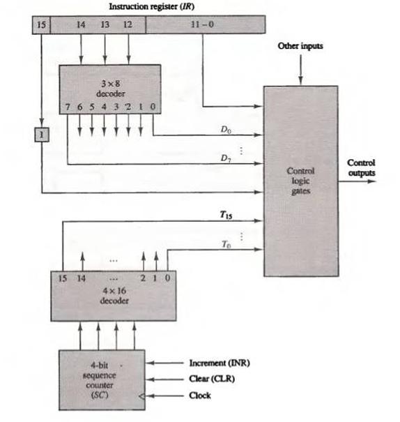
Derive the Boolean expression for the gate structure that clears the sequence counter SC to 0. Draw the logic diagram of the gates and show how the output is connected to the INR and CLR inputs of SC (see Fig. 5-6). Minimize the number of gates.Fig. 5-6 15 Instruction register (IR) 14 13
Show the complete logic of the interrupt flip-flops R in the basic computer. Use a JK flip-flop and minimize the number of gates.
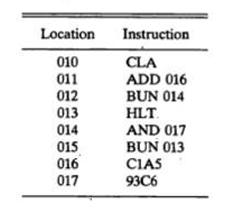
The following program is stored in the memory unit of the basic computer. Show the contents of the AC, PC, and IR (in hexadecimal), at the end, after each instruction is executed. All numbers listed below are in hexadecimal. Location 010 011 012 013 014 015 016 017 Instruction CLA ADD 016 BUN
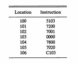
The following program is a list of instructions in hexadecimal code. The computer executes the instructions starting from address 100. What are the content of AC and the memory word at address 103 when the computer halts?
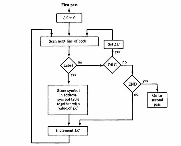
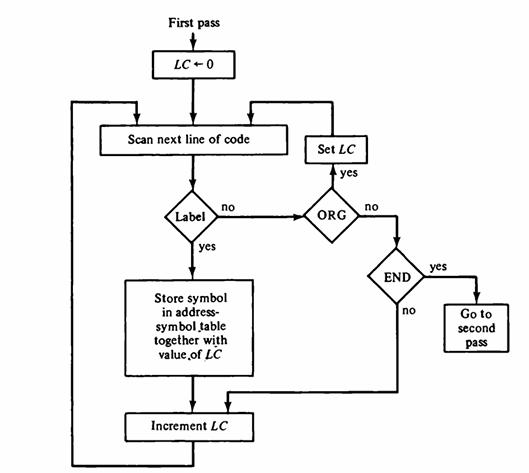
What happens during the first pass of the assembler (Fig. 6-1) if the line of code that has a pseudoinstruction ORG or END also has a label? Modify the flowchart to include an error message if this occurs.Fig. 6-1 First pass LC+0 Scan next line of code Label yes no Store symbol in address- symbol
List the assembly language program (of the equivalent binary instructions) generated by a compiler from the following Fortran program. Assume integer variables.SUM = 0 SUM = SUM + A + B DIF = DIF - CSUM = SUM + DIF
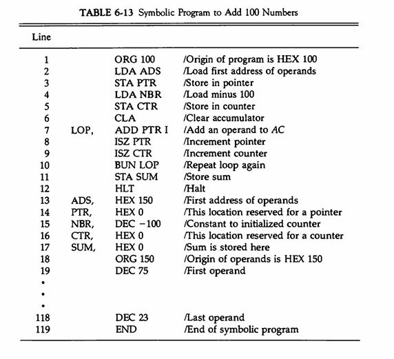
a. Obtain the address symbol table generated for the program of Table 6-13 during the first pass of the assembler. b. List the translated program in hexadecimal.Table 6-13 Line 1 2 3 4 5 56 6 7 8 10 11 12 13 14 15 16 17 18 19 TABLE 6-13 Symbolic Program to Add 100 Numbers 118 119 LOP, ADS, PTR, 15
Can the letter I be used as a symbolic address in the assembly language program defined for the basic computer? Justify the answer.
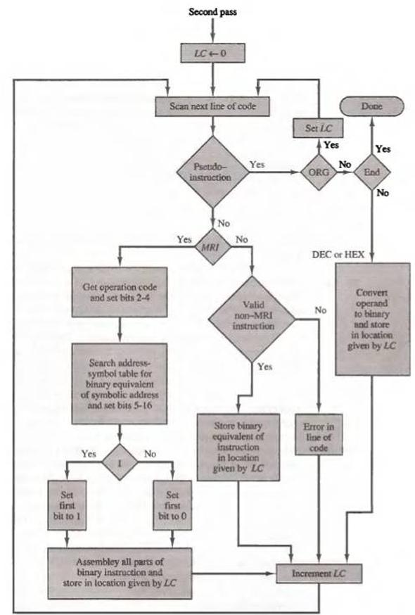
Modify the flowchart of Fig. 6-2 to include an error message when a symbolic address is not defined by a label.Fig. 6-2 Set first bit to 1 Get operation code and set bits 2-4 Search address- symbol table for binary equivalen of symbolic address and set bits 5-16 Yes No Second pass Scan next line of
A line of code in an assembly language program is as follows: DEC - 35a. Show that four memory words are required to store the line of code and give their binary content. b: Show that one memory word stores the binary translated code and give its binary content.
The pseudoinstruction BSS N (block started by symbol) is sometimes employed to reserve N memory words for a group of operands. For example, the line of code A, BSS 10 informs the assembler. that a block of 10 (decimal) locations is to be left free, starting from location A. This is similar to the
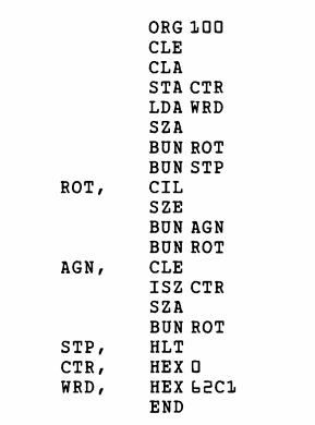
a. Explain in words what the following program accomplishes when it is executed. What is the value of location CTR when the computer halts? b. List the address symbol table obtained during the first pass of the assembler. c. List the hexadecimal code of the translated program.
Show how the MRI and non-MRI tables can be stored in memory.
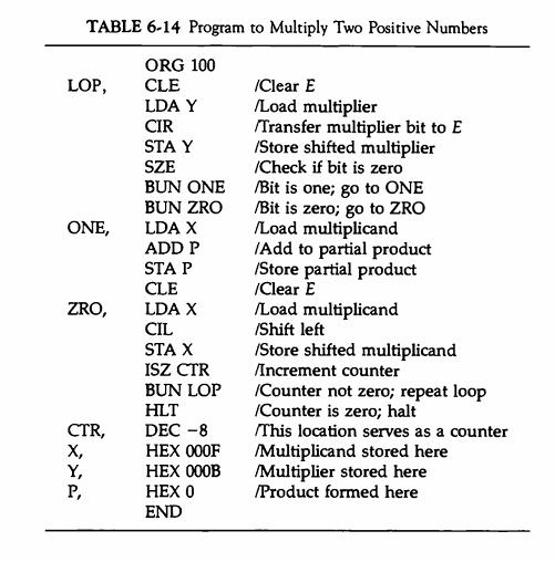
The multiplication program of Table 6-14 is not initialized. After the program is executed once, location CTR will be left with zero. Show that if the program is executed again starting from location 100, the loop will be traversed 65536 times. Add the needed instructions to initialize the
List the assembly language program (of the equivalent binary instructions) generated by a compiler for the following IF statement: IF (A - B) 10, 20, 30 The program branches to statement 10 if A - B < 0; to statement 20 if A - B = 0; and to statement 30 if A - B > 0.
Write a program loop, using a pointer and a counter, that clears to 0 the contents of hexadecimal locations 500 through 5FF.
Write a program to multiply two positive numbers by a repeated addition method. For example, to multiply 5 x 4, the program evaluates the product by adding 5 four times, or 5 + 5 + 5 + 5.
Write a program to multiply two unsigned positive numbers, each with 16 significant bits, to produce an unsigned double-precision product.
Write a program to multiply two signed numbers with negative numbers being initially in signed-2's complement representation. The product should be single-precision and signed-2's complement representation if negative.
Write a program to subtract two double-precision numbers.
Write a program that evaluates the logic exclusive-OR of two logic operands.
Write a program for the arithmetic shift-left operation. Branch to OVF if an overflow occurs.
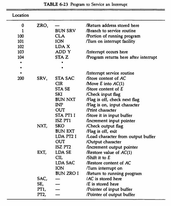
Translate the service routine SRV from Table 6-23 to its equivalent hexadecimal code. Assume that the routine is stored starting from location 200.Table 6-23 Location 0 1 100 101 102 103 104 200 TABLE 6-23 Program to Service an Interrupt ZRO, SRV, STA SAC CIR STA SE SKI BUN NXT INP NXT, EXT, BUN
Write a subroutine to subtract two numbers. In the calling program, the BSA instruction is followed by the subtrahend and minuend. The difference is returned to the main program in the third location following the BSA instruction.
Write a subroutine to complement each word in a block of data. In the calling program, the BSA instruction is followed by two parameters: the starting address of the block and the number of words in the block.
Write a subroutine to circulate E and AC four times to the right. If AC contains hexadecimal 079C and E= 1, what are the contents of AC and E after the subroutine is executed?
Write a program to accept input characters, pack two characters in one word and store them in consecutive locations in a memory buffer. The first address of the buffer is (400)16. The size of the buffer is (512)10 words. If the buffer overflows, the computer should halt.
Write an interrupt service routine that performs all the required functions but the input device is serviced only if a special location, MOD, contains all 1's. The output device is serviced only if location MOD contains all 0's.
What is the difference between a microprocessor and a microprogram? Is it possible to design a microprocessor without a microprogram? Are all microprogrammed computers also microprocessors?
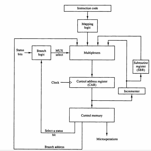
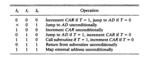
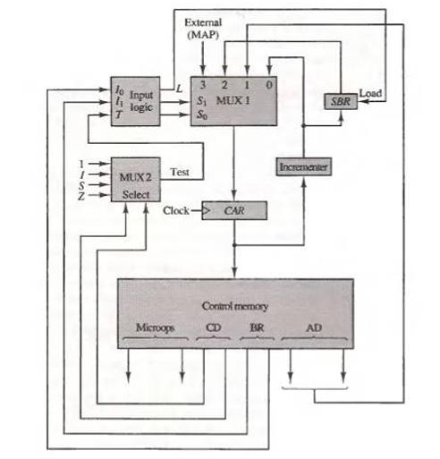
The system shown in Fig. 7-2 uses a control memory of 1024 words of 32 bits each. The microinstruction has three fields as shown in the diagram. The microoperations field has 16 bits. a. How many bits are there in the branch address field and the select field?b. If there are 16 status bits in the
Explain the difference between hardwired control and microprogrammed control. Is it possible to have a hardwired control associated with a control memory?
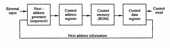
The microprogrammed control organization shown in Fig. 7-1 has the following propagation delay times. 40 ns to generate the next address, 10 ns to transfer the address into the control address register, 40 ns to access the control memory ROM, 10 ns to transfer the microinstruction into the control
Define the following: (a) Microoperation; (b) Microinstruction; (c) Micro- program; (d) Microcode.
The control memory in Fig. 7-2 has 4096 words of 24 bits each. a. How many bits are there in the control address register? b. How many bits are there in each of the four inputs shown going into the multiplexers? c. What are the number of inputs in each multiplexer and how many multiplexers are
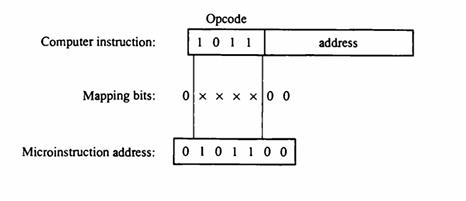
Using the mapping procedure described in Fig. 7-3, give the first microinstruction address for the following operation code: (a) 0010; (b) 1011; (c) 1111.Fig. 7-3 Computer instruction: Mapping bits: Microinstruction address: Opcode 1011 0x x x x 0 0 0101100 address
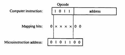
Explain how the mapping from an instruction code to a microinstruction address can be done by means of a read-only memory. What is the advantage of this method compared to the one in Fig. 7-3?Fig. 7-3 Computer instruction: Mapping bits: Microinstruction address: Opcode 1011 0x x x x00 01
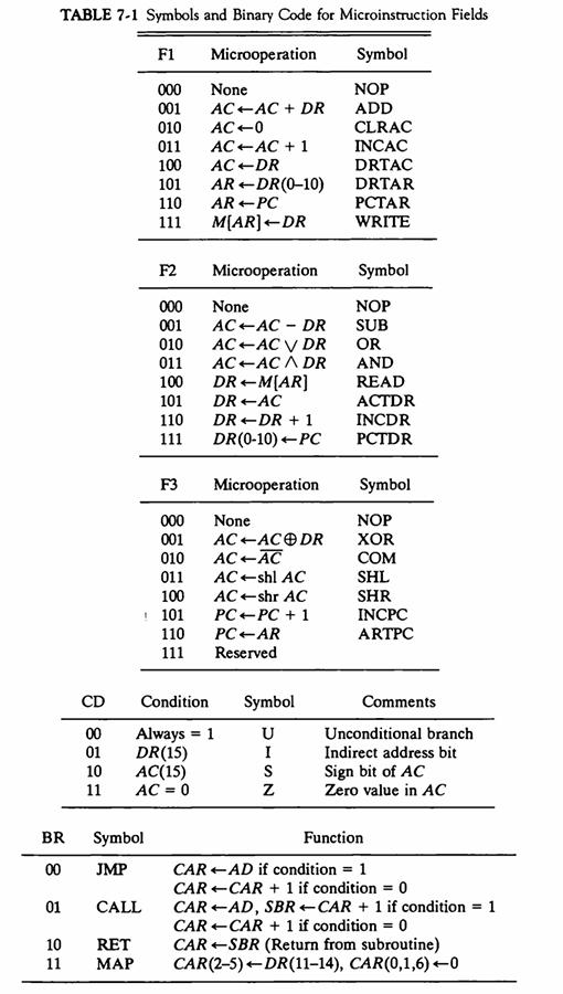
Using Table 7-1, give the 9-bit microoperation field for the following microoperations: a. AC←AC + 1, DR←DR + 1 b. PC←PC + 1, DR←M[AR] c. DR←AC, AC←DRTable 7-1 TABLE 7-1 Symbols and Binary Code for Microinstruction
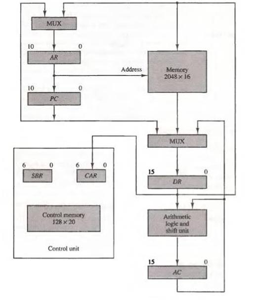
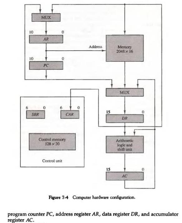
Why do we need the two multiplexers in the computer hardware configuration shown in Fig. 7-4? Is there another way that information from multiple sources can be transferred to a common destination?Fig. 7-4 HI 10 10 SBR MUX AR PC CAR Control memory 128 x 20 Control unit Address 15 15 Memory 2048 x
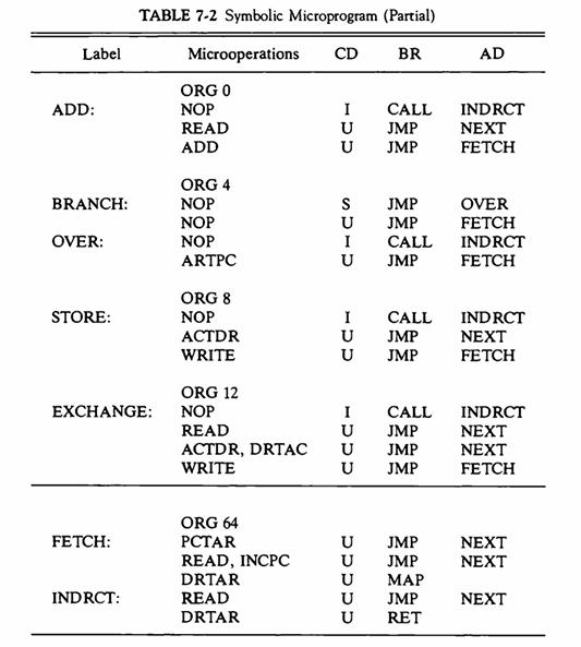
Add the following instructions to the computer of Sec 7-3 (EA is the effective address). Write the symbolic microprogram for each routine as in Table 7-2. (Note that AC must not change in value unless the instruction specifies a change in AC.)Table 7-2 Symbol Opcode AND 0100 AC
Formulate a mapping procedure that provides eight consecutive microinstructions for each routine. The operation code has six bits and the control memory has 2048 words.
Using Table 7-1, convert the following symbolic microoperations to register transfer statements and to binary. a. READ, INCPC b. ACTDR, DRTAC c. ARTPC, DRTAC, WRITETable 7-1 TABLE 7-1 Symbols and Binary Code for Microinstruction
Suppose that we change the ADD routine listed in Table 7-2 to the following two microinstructions. ADD: READ I CALL INDR2 ADD U JMP FETCHWhat should be subroutine INDR2? Table 7-2
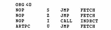
The following is a symbolic microprogram for an instruction in the computer defined in Sec. 7-3.a. Specify the operation performed when the instruction is executed. b. Convert the four microinstructions into their equivalent binary form. ORG
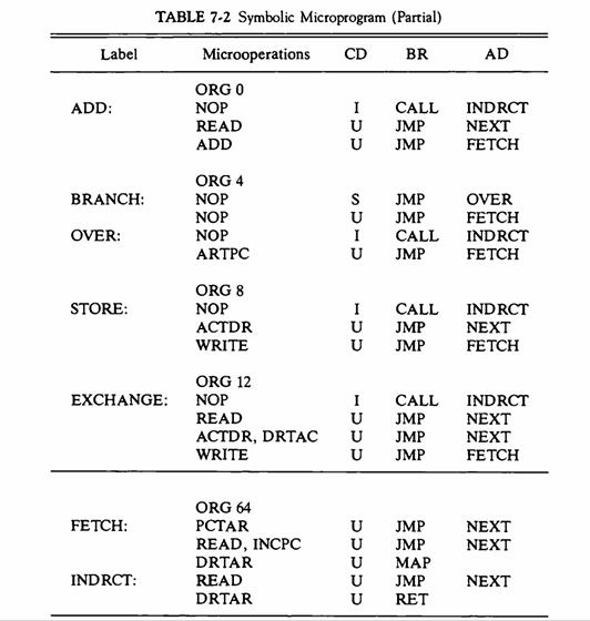
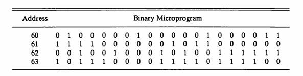
The computer of Sec. 7-3 has the following binary microprogram:a. Translate it to a symbolic microprogram as in Table 7-2. (FETCH is in address 64 and INDRCT in address 67.) b. List all the things that will be wrong when this microprogram is executed in the computer.Table 7-2
Write a symbolic microprogram routine for the ISZ (increment and skip if zero) instruction defined in Chap. 5 (Table 5-4). Use the microinstruction format of Sec. 7-3. Note that DR = 0 status condition is not available in the CD field of the computer defined in Sec. 7-3. However, you can exchange
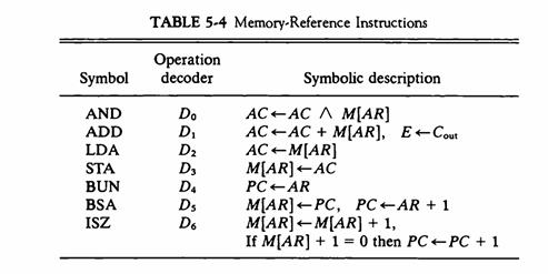
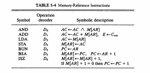
Write the symbolic microprogram routines for the BSA (branch and save address) instructions defined in Chap. 5 (Table 5-4). Use the microinstruction format of Sec. 7-3. Minimize the number of microinstructions.Table 5-4 Symbol AND ADD LDA STA BUN BSA ISZ TABLE 5-4 Memory-Reference
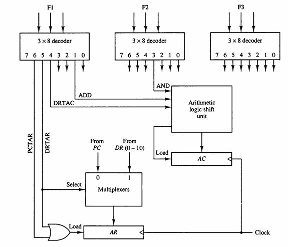
Show how outputs 5 and 6 of decoder F3 in Fig. 7-7 are to be connected to the program counter PC.Fig. 7-7 FI PCTAR 3 x 8 decoder 7 6 5 4 3 210 DRTAR DRTAC ADD Select Load From PC 0 F2 Multiplexers AR 3 x 8 decoder 7 6 5 4 3 2 10 From DR (0-10) AND Load Arithmetic logic shift unit AC F3 3 x 8
A computer has 32-bit instructions and 12-bit addresses. If there are 250 two-address instructions, how many one-address instructions can be formulated?
Show how a 9-bit microoperation field in a microinstruction can be divided into subfields to specify 46 microoperations. How many microoperations can be specified in one microinstruction?
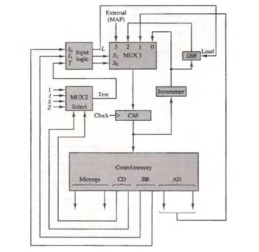
Assume that the input logic of the microprogram sequencer of Fig. 7-8 has four inputs, I2, I1, I0 T (test), and three outputs, S1, S0, and L. The operations that are performed in the unit are listed in the following table. Design the input logic circuit using a minimum number of gates.Fig. 7-8 1₂
Design a 7-bit combinational circuit incrementer for the microprogram sequencer of Fig. 7-8 (see Fig. 4-8). Modify the incrementer by including a control input D. When D= 0, the circuit increments by one, but when D 1, the circuit increments by two.Fig. 7-8Fig. 4-8
A computer has 16 registers, an ALU (arithmetic logic unit) with 32 operations, and a shifter with eight operations, all connected to a common bus system. a. Formulate a control word for a microoperation. b. Specify the number of bits in each field of the control word and give a general encoding
Insert an exclusive-OR gate between MUX 2 and the input logic of Fig. 7-8. One input to the gate comes from the test output of the multiplexer. The other input to the gate comes from a bit labeled P (for polarity) in the microinstruction from control memory. The output of the gate goes to the input
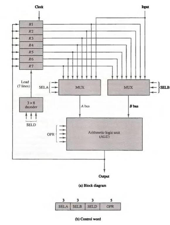
A bus-organized CPU similar to Fig. 8-2 has 16 registers with 32 bits in each, an ALU, and a destination decoder. a. How many multiplexers are there in the A bus, and what is the size of each multiplexer? b. How many selection inputs are needed for MUX A and MUX B? c. How many inputs and outputs
The bus system of Fig. 8-2 has the following propagation delay times: 30 ns for the signals to propagate through the multiplexers, 80 ns to perform the ADD operation in the ALU, 20 ns delay in the destination decoder, and 10 ns to clock the data into the destination register. What is the minimum
Specify the control word that must be applied to the processor of Fig. 8-2 to implement the following microoperations. a. R1←R2 + R3b. R4←R4 c. R5←R5 - 1 d. R6←inputFig. 8-2 R1 R2 R3 R4 R5 R6 R7 Load (7 lines) Clock 3x8 decoder SELD SELA OPR | | | | | MUX A bus Arithmetic logic
Determine the microoperations that will be executed in the processor of Fig. 8-2 when the following 14-bit control words are applied. a. 00101001100101 b. 00000000000000 c. 01001001001100 d. 00000100000010 e. 11110001110000Fig. 8-2 R1 R2 R3 R4 R5 R6 R7 Load (7
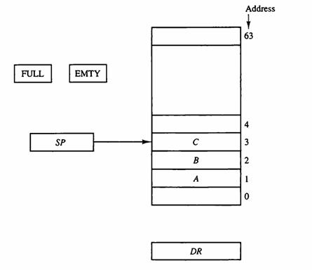
Let SP = 000000 in the stack of Fig. 8-3. How many items are there in the stack if: a. FULL = 1 and EMTY = 0?b. FULL = 0 and EMTY = 1?Fig. 8-3 FULL SP EMTY C B A DR Address 63 4 3 2 1 0
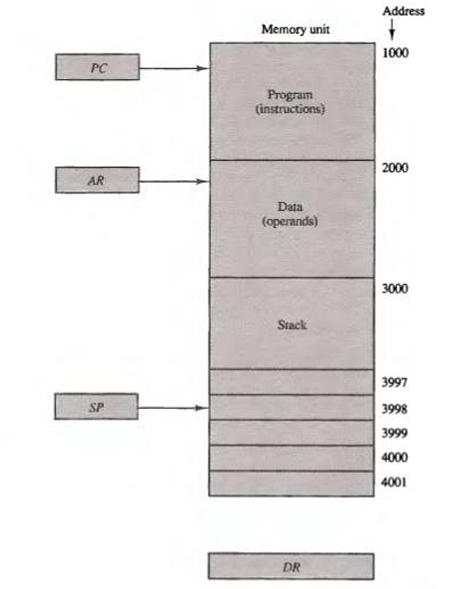
A stack is organized such that SP always points at the next empty location on the stack. This means that SP can be initialized to 4000 in Fig. 8-4 and the first item in the stack is stored in location 4000. List the microoperations for the push and pop operations.Fig. 8-4 PC AR SP Memory
Convert the following arithmetic expressions from infix to reverse Polish notation. a. A B + C D + E*F b. A B + A*(B*D + C*E) c. A + B* [CD+E * (F + G)] A [B+C (D + E)] F* (G + H) d.
Convert the following arithmetic expressions from reverse Polish notation to infix notation. a. A B C D E + * - / b. A B C D E * / - + c. A B C * / D - E F / + d. A B C D E F G + * + * + *
Convert the following numerical arithmetic expression into reverse Polish notation and show the stack operations for evaluating the numerical result. (3 + 4)[10(2 + 6) + 8]
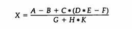
Write a program to evaluate the arithmetic statement:a. Using a general register computer with three address instructions. b. Using a general register computer with two address instructions. c. Using an accumulator type computer with one address instructions. d. Using a stack organized computer
A first-in, first-out (FIFO) has a memory organization that stores information in such a manner that the item that is stored first is the first item that is retrieved. Show how a FIFO memory operates with three counters. A write counter WC holds the address for writing into memory. A read counter
The memory unit of a computer has 256K words of 32 bits each. The computer has an instruction format with four fields: an operation code field, a mode field to specify one of seven addressing modes, a register address field to specify one of 60 processor registers, and a memory address. Specify the
A relative mode branch type of instruction is stored in memory at an address equivalent to decimal 750. The branch is made to an address equivalent to decimal 500. a. What should be the value of the relative address field of the instruction (in decimal)? b. Determine the relative address value in
How many times does the control unit refer to memory when it fetches and executes an indirect addressing mode instruction if the instruction is (a) A computational type requiring an operand from memory;(b) A branch type.
What must the address field of an indexed addressing mode instruction be to make it the same as a register indirect mode instruction?
An instruction is stored at location 300 with its address field at location 301. The address field has the value 400. A processor register R1 contains the number 200. Evaluate the effective address if the addressing mode of the instruction is (a) Direct; (b) Immediate; (c) Relative; (d)
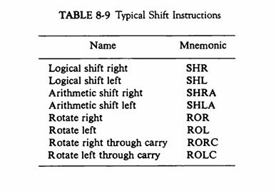
An 8-bit register contains the value 01111011 and the carry bit is equal to 1. Perform the eight shift operations given by the instructions listed in Table 8-9. Each time, start from the initial value given above.Table 8-9 TABLE 8-9 Typical Shift Instructions Name Logical shift right Logical shift
Assuming an 8-bit computer, show the multiple precision addition of the two 32-bit unsigned numbers listed below using the add with carry instruction. Each byte is expressed as a two-digit hexadecimal number. (6E C3 56 7A) + (13 55 6B 8F)
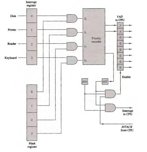
What should be done in Fig. 11-14 to make the four VAD values equal to the binary equivalent of 76, 77, 78, and 79?Fig. 11-14 Disk Printer Reader Keyboard Interrupt register 0 Ci لم 0 - N Mask register lo 1₁ h HEN Priority encoder IST VAD to CPU 0 0 0000 Enable Interrupt to CPU INTACK from CPU
Perform the logic AND, OR, and XOR with the two binary strings 10011100 and 10101010.
Given the 16-bit value 1001101011001101. What operation must be performed in order to: a. Clear to 0 the first eight bits? b. Set to 1 the last eight bits? c. Complement the middle eight bits?
Represent the following signed numbers in binary using eight bits. +83; -83; +68; -68. a. Perform the addition (-83) + (+68) in binary and interpret the result obtained. b. Perform the subtraction (-68) - (+83) in binary and indicate if there is an overflow. c. Shift binary -68 once to the right
A two-word instruction is stored in memory at an address designated by the symbol W. The address field of the instruction (stored at W + 1) is designated by the symbol Y. The operand used during the execution of the instruction is stored at an address symbolized by Z. An index register contains the
A computer uses RAM chips of 1024 x 1 capacity. a. How many chips are needed, and how should their address lines be connected to provide a memory capacity of 1024 bytes? b. How many chips are needed to provide a memory capacity of 16K bytes? Explain in words how the chips are to be connected to
An 8-bit computer has a 16-bit address bus. The first 15 lines of the address are used to select a bank of 32K bytes of memory. The high-order bit of the address is used to select a register which receives the contents of the data bus. Explain how this configuration can be used to extend the memory
A magnetic disk system has the following parameters: Ts = average time to position the magnetic head over a track R = rotation speed of disk in revolutions per second Nt = number of bits per track Ns = number of bits per sector Calculate the average time Ta that it will take to read one sector.
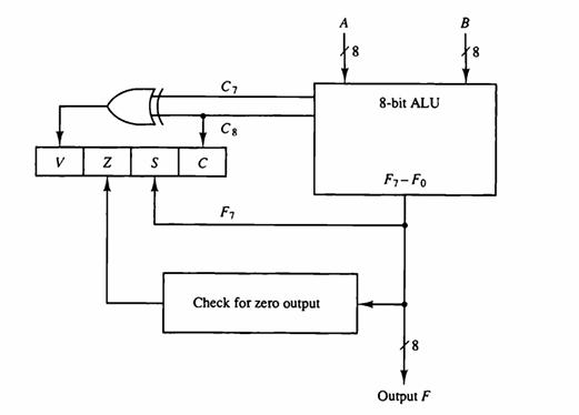
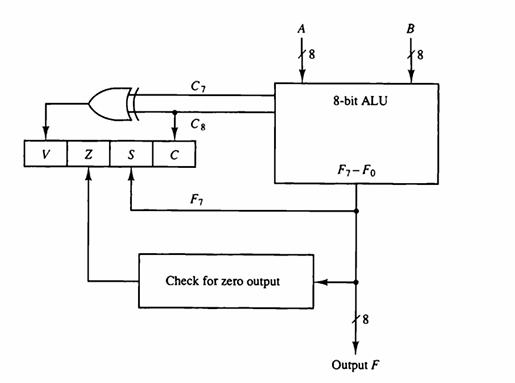
Show that the circuit labeled "check for zero output" in Fig. 8-8 is an 8-bit NOR gate.Fig. 8-8 V N S C C7 F₁ Check for zero output 8-bit ALU F₁-Fo 8 Output F B 8
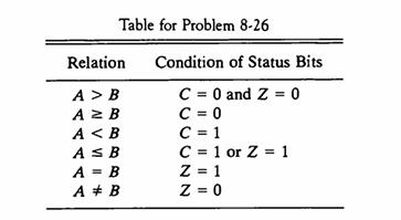
Two signed numbers A and B represented in signed-2's complement form are compared by subtracting A - B. Status bits S, Z, and V are set or cleared depending on the result of the operation. (Note that there is a sign reversal if an overflow occurs.) Show that the relative magnitude of A and B can be
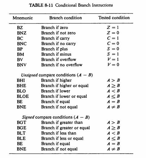
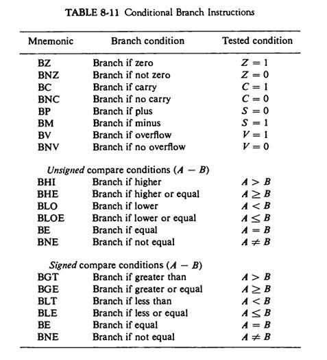
Two unsigned numbers A and B are compared by subtracting A - B. The carry status bit is considered as a borrow bit after a compare instruction in most commercial computers, so that C = 1 if A Table 8-11 Mnemonic BZ BNZ BC BNC BP BM BV BNV TABLE 8-11 Conditional Branch
An 8-bit computer has a register R. Determine the values of status bits C, S, Z, and V (Fig. 8-8) after each of the following instructions. The initial value of register R in each case is hexadecimal 72. The numbers below are also in hexadecimal. a. Add immediate operand C6 to R. b. Add immediate
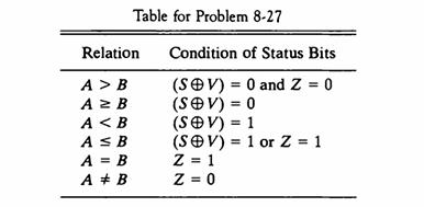
It is necessary to design a digital circuit with four inputs C, S, Z, and V and 10 outputs, one for each of the branch conditions listed in Probs. 8-26 and 8-27. (The equal and unequal conditions are common to both tables.) Draw the logic diagram of the circuit using two OR gates, one XOR gate, and
Consider the two 8-bit numbers A = 01000001 and B = 10000100. a. Give the decimal equivalent of each number assuming that (1) they are unsigned, and (2) they are signed. b. Add the two binary numbers and interpret the sum assuming that the numbers are (1) unsigned, and (2) signed. c. Determine
Showing 100 - 200
of 330
1
2
3
4
Step by Step Answers
![Symbol Opcode Symbolic designation XOR ADM 000 AC ACM[EA] 001 M[EA] M[EA] + AC AC ACM[EA] SUB XCH SEQ BPA 010](https://dsd5zvtm8ll6.cloudfront.net/images/question_images/1697/8/9/6/4226533d7e6b06161697896421310.jpg)

![Symbol Opcode AND 0100 AC AC SUB ADM BTCL Symbolic Function AM[EA] 0101 AC ACM[EA] 0110 M[EA] M[EA] + AC AC](https://dsd5zvtm8ll6.cloudfront.net/images/question_images/1698/0/4/1/28365360dc3e2fa41698041250424.jpg)


![a. A B + C D + E*F b. A B + A*(B*D + C*E) c. A + B* [CD+E * (F + G)] A [B+C (D + E)] F* (G + H) d.](https://dsd5zvtm8ll6.cloudfront.net/images/question_images/1698/0/4/3/494653616663efb61698043490620.jpg)