New Semester
Started
Get
50% OFF
Study Help!
--h --m --s
Claim Now
Question Answers
Textbooks
Find textbooks, questions and answers
Oops, something went wrong!
Change your search query and then try again
S
Books
FREE
Study Help
Expert Questions
Accounting
General Management
Mathematics
Finance
Organizational Behaviour
Law
Physics
Operating System
Management Leadership
Sociology
Programming
Marketing
Database
Computer Network
Economics
Textbooks Solutions
Accounting
Managerial Accounting
Management Leadership
Cost Accounting
Statistics
Business Law
Corporate Finance
Finance
Economics
Auditing
Tutors
Online Tutors
Find a Tutor
Hire a Tutor
Become a Tutor
AI Tutor
AI Study Planner
NEW
Sell Books
Search
Search
Sign In
Register
study help
engineering
electronics fundamentals a systems approach
Electronics Fundamentals A Systems Approach 1st Edition Thomas Floyd - Solutions
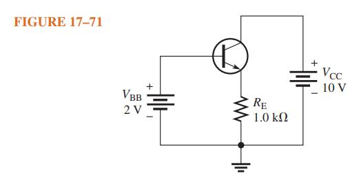
Determine the emitter voltage with respect to ground in Figure 17–71. FIGURE 17-71 VBB 2 V |||| RE 1.0 ΚΩ + Vcc 10 V
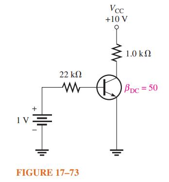
Determine IB, IC, and VC in Figure 17–73. IV 22 ΚΩ Μ FIGURE 17-73 Vcc +10 V Φ 1.0 ΚΩ |8bc = 50
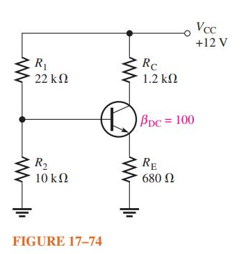
For the circuit in Figure 17–74, find VB, VE, IE, IC, and VC. R₁ 22 ΚΩ R₂ 10 ΚΩ FIGURE 17-74 Rc 1.2 ΚΩ |βpc = 100 RE 680 Ω Vcc +12V
In Figure 17–74, what is VCE? What are the Q-point coordinates? R₁ • 22 ΚΩ R₂ 10 ΚΩ FIGURE 17-74 Rc 1.2 ΚΩ | βpc = 100 RE 680 Ω HI Vcc +12V
A transistor amplifier has a voltage gain of 50. What is the output voltage when the input voltage is 100 mV?
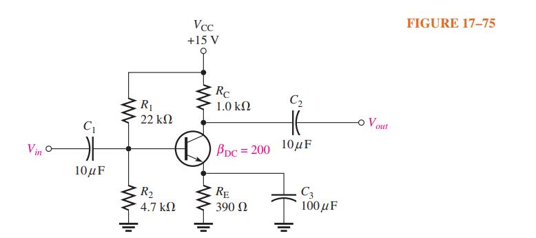
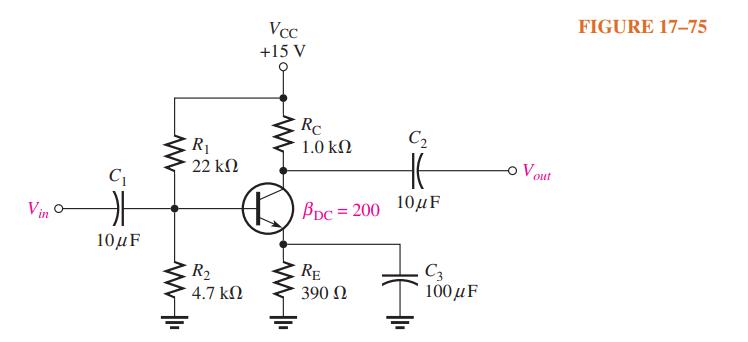
Determine the voltage gain for Figure 17–75. Vin C₁ Η 10μF R₁ 22 ΚΩ R₂ 4.7 ΚΩ Vcc +15 V Rc 1.0 ΚΩ C HE βpc=200 10μF RE 390 Ω C3 100 με -o Vout FIGURE 17–75
To achieve an output of 10 V with an input of 300 mV, what voltage gain is required?
Determine each of the dc voltages, VB, VC, and VE, with respect to ground in Figure 17–75. Vin C₁ 10μF WI R₁ 22 ΚΩ R₂ 4.7 ΚΩ Vcc +15 V Rc 1.0 ΚΩ C₂ PDC=200 10μF RE 390 Ω C3 100 μF o Vout FIGURE 17-75
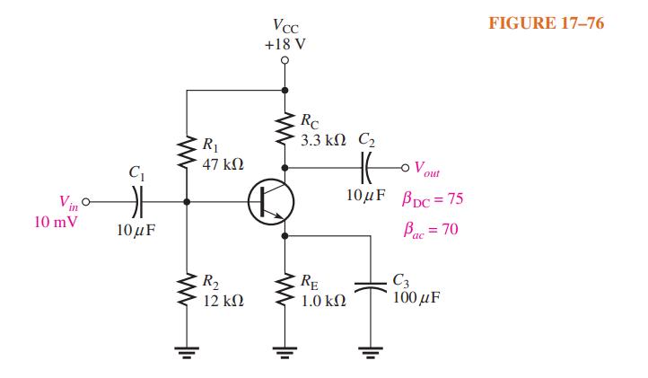
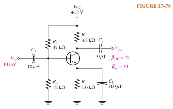
Determine the following dc values for the amplifier in Figure 17–76:(a) VB (b) VE (c) IE (d) IC (e) VC (f) VCE 10 mV C₁ 카 10 μF www R₁ 47 ΚΩ R₂ 12 ΚΩ Vcc +18 V Rc 3.3 ΚΩ C2 HE O V RE 1.0 ΚΩ out 10μF PDC=75 Bac = 70 C3 100 μF FIGURE 17-76
Determine the following ac values for the amplifier in Figure 17–76:(a) Rin (b) Rin(tot) (c) Av (d) Ai (e) Ap Vin 10 mV C₁ F 10 μF R₁ 47 ΚΩ R₂ 12 ΚΩ Vcc +18 V Rc 3.3 ΚΩ C2 -OV out HE 10μF BDC = 75 Bac = 70 RE 1.0 ΚΩ C3 100 μF FIGURE 17-76
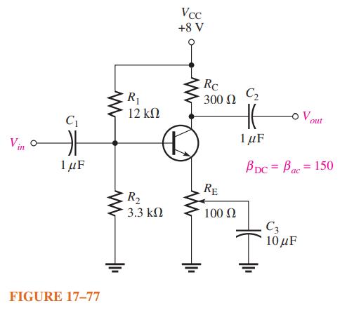
If a load resistance of 600 Ω is placed on the output of the amplifier in Figure 17–77, what is the maximum gain? Vin C₁ 카 1 μF FIGURE 17-77 www R₁ 12 ΚΩ R₂ 3.3 ΚΩ Vcc +8 V +₁ Rc 300 Ω RE 100 Ω C₂ HE 1 μF BDC = Bac = 150 -O V out C3 10 μF
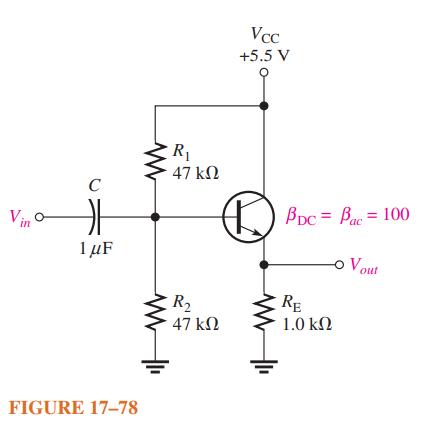
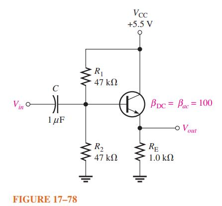
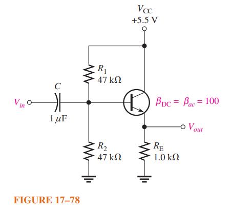
Determine the voltage gain for the emitter-follower in Figure 17–78. Vino C 1 μF FIGURE 17-78 R₁ 47 ΚΩ R₂ 47 ΚΩ Vcc +5.5 V RBDC = BDC = Bac=100 RE 1.0 ΚΩ o Vout
What is the total input resistance in Figure 17–78? What is the dc output voltage? Π C 1 μF FIGURE 17-78 R₁ • 47 ΚΩ R₂ • 47 ΚΩ Vcc +5.5 V βbc = βa = 100 Bac -o Vout RE 1.0 ΚΩ
A load resistance is capacitively coupled to the emitter in Figure 17–78. In terms of signal operation, the load appears in parallel with RE and reduces the effective emitter resistance. How does this affect the voltage gain? in C Η 1μF FIGURE 17-78 R₁ 47 ΚΩ R₂ 47 ΚΩ Vcc +5.5 V ( Boc=
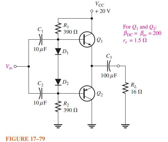
Determine the dc voltages at the bases and emitters of Q1 and Q2 in Figure 17–79. Also determine VCEQ for each transistor. C₁ 10 μF C₂ F 10 μF FIGURE 17-79 R₁ 390 Ω D₁ D₂ R₂ 390 Ω Vcc + 20 V 2₁ C3 100 μF De₂ For Q₁ and Q₂: PDC = Bac 200 Te = 1.50 RL 16 Ω
Determine the maximum peak output voltage and peak load current for the circuit in Figure 17–79. Vin C₁ 10 μF C₂ 10 μF FIGURE 17-79 R₁ 390 Ω www D₁ D₂ R₂ 390 02 Vcc + 20 V Q₁ C3 HE 100 μF 2₂ For Q₁ and Q₂: PDC = Bac=200 Te = 1.50 RL 16 Ω
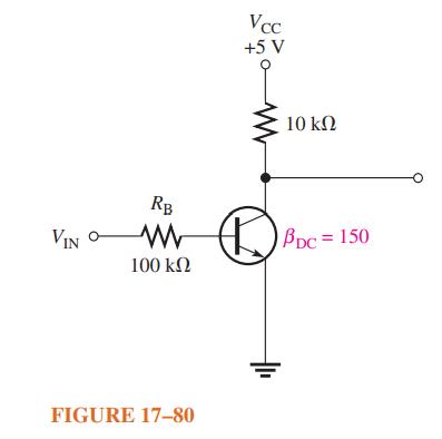
Determine IC(sat) for the transistor in Figure 17–80. What is the value of IB necessary to produce saturation? What minimum value of VIN is necessary for saturation? VIN α RB Μ 100 ΚΩ FIGURE 17-80 α Vcc +5 V 10 ΚΩ |8bc = 150
The efficiency of a certain class B push-pull amplifier is 0.71, and the dc input power is 16.3 W. What is the ac output power?
The VGS of a p-channel JFET is increased from 1 V to 3 V.(a) Does the depletion region narrow or widen? (b) Does the resistance of the channel increase or decrease?
Why must the gate-to-source voltage of an n-channel JFET always be either 0 V or negative?
Draw the schematic symbols for n -channel and p-channel D-MOSFETs and E-MOSFETs. Label the terminals.
Explain why both types of MOSFETs have an extremely high input resistance at the gate.
In what mode is an n-channel D-MOSFET operating with a positive VGS?
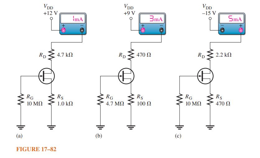
For each circuit in Figure 17–82, determine VDS and VGS. (a) VDD +12 V RD RG 10 FIGURE 1782 +0 4.7 Rs 1.0 ImA (b) VDD +9 V RD RG 4.7 +O 470 Rs 100 3mA (c) VDD -15 V RD RG 10 SMA 2.2 Rs 470 +O
A certain E-MOSFET has a VGS(th) = 3 V. What is the minimum VGS for the device to turn on?
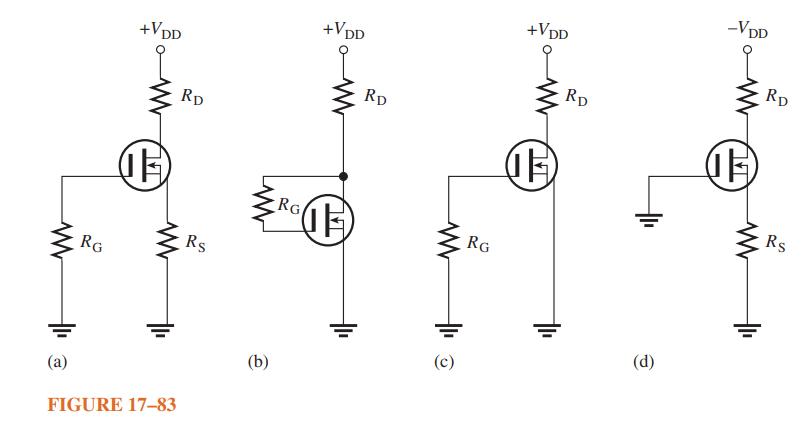
Determine in which mode (depletion or enhancement) each D-MOSFET in Figure 17–83 is biased. www RG +VDD (E T FIGURE 17-83 RD Rs (b) RG +VDD F RD www the RG +VDD IL RD (d) -VDD HD RD Rs
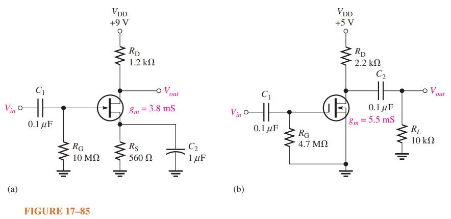
Determine the voltage gain of each CS amplifier in Figure 17–85. Vin' (a) C₁ 0.1 μF RG 10 ΜΩ FIGURE 17-85 VDD +9 V B RD 1.2 ΚΩ V out 8m = 3.8 ms Rs 560 Ω C₂ 1 μF Vin (b) C₁ 0.1 μF RG 4.7 ΜΩ VDD +5 V F RD 2.2 ΚΩ C₂ 0.1 μF 8m = 5.5 mS Vau R₁ 10 ΚΩ out
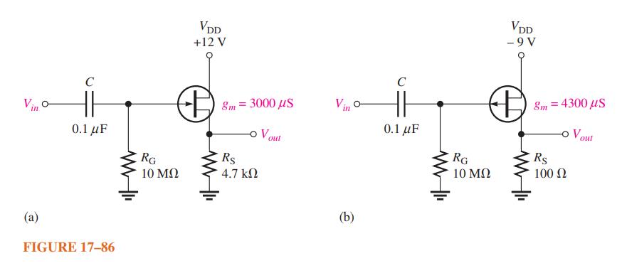
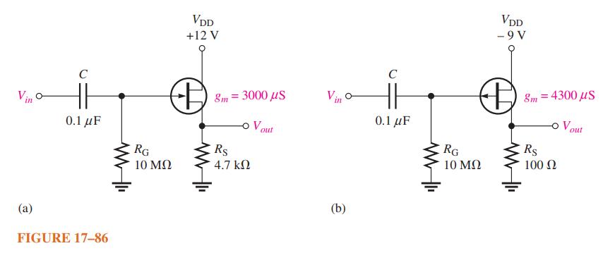
Find the gain of each amplifier in Figure 17–86. (a) C 0.1 μF FIGURE 17-86 RG 10 ΜΩ VDD +12 V (B) 8m = 3000 μs -o Vout Rs 4.7 ΚΩ Vino (b) C 0.1 μF RG 10 ΜΩ VDD - 9 V + 8m = 4300 μs Rs 100 Ω Vout
Determine the gain of each amplifier in Figure 17–86 when a 10 kΩ load is capacitively coupled from source to ground. Vin (a) C 0.1 μF FIGURE 17-86 VDD +12 V C RG 10 ΜΩ 8m = 3000 μs OV out Rs 4.7 ΚΩ (b) C 0.1 μF RG 10 ΜΩ VDD - 9 V O WWII 8m=4300 μs Rs 100 Ω Vou out
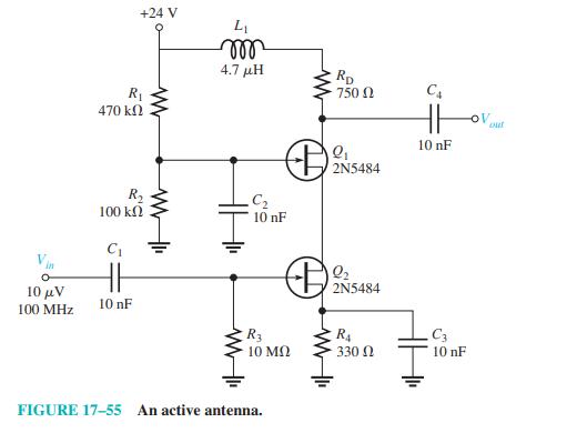
In Figure 17–55, what is the input resistance presented to the antenna? Assume IGSS = 1.0 nA and ID = 2.0 mA. in 10 μV 100 MHz 470 ΚΩ R₁ C₁ 100 ΚΩ +24 V R₂ 10 nF L₁ mo 4.7 μΗ + C₂ 10 nF FIGURE 17-55 An active antenna. R3 10 ΜΩ RD • 750 Ω Q₁ 2N5484 Boe 2N5484 R₁ 330
If the voltage gain of the amplifier portion of a feedback oscillator is 75, what must be the attenuation of the feedback circuit to sustain the oscillation?
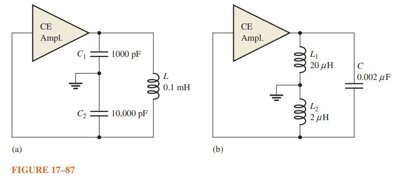
Calculate the frequency of oscillation for each circuit in Figure 17–87 and identify each type of oscillator. (a) CE Ampl. FIGURE 17-87 C₁ C₂ 1000 pF 10,000 pF L 0.1 mH (b) CE Ampl. L₁ 20 μΗ 12 2 μΗ C 0.002 μF
Generally describe the change required to the oscillator of Problem 43 in order for oscillation to begin when the power is initially turned on. Data in Problem 43If the voltage gain of the amplifier portion of a feedback oscillator is 75, what must be the attenuation of the feedback circuit to
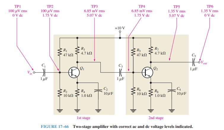
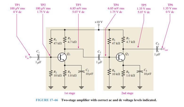
Assume that R5 opens in Figure 17–66. Will Q2 be in cutoff or in conduction? What dc voltage will you observe at the Q2 collector? ΤΡΙ 100 μV rms 0V de Vino TP2 100 μV rms 1.75 V de C₁ F 1 μF www www R₁ 47 ΚΩ R₂ 10 ΚΩ www TP3 6.85 mV rms 5.07 V de R3 4.7 ΚΩ a Q₁ R₁ 1.0
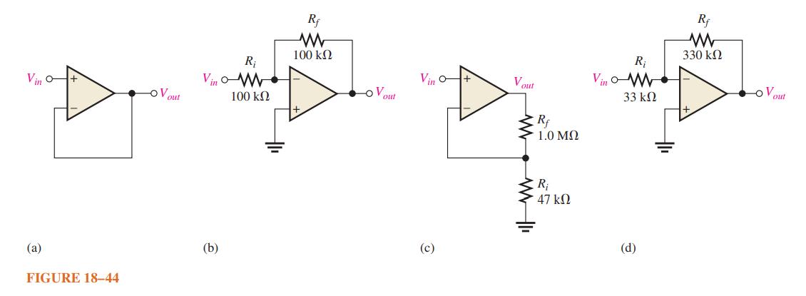
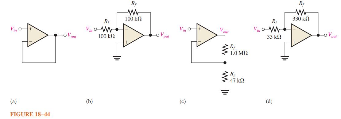
Find the gain of each amplifier in Figure 18–44. Vin o (a) FIGURE 18-44 -OV out Vin (b) R 100 Rf www 100 - Vout Vino- + Vout WWII Rf 1.0 R 47 Vino R 33 (d) Rf www 330 -o Vout
Describe the process of doping and explain how it alters the atomic structure of silicon.
What type of impurity is antimony? What type of impurity is boron?
Explain what a hole is.
What is recombination?
How is the electric field across the pn junction created?
Because of its barrier potential, can a diode be used as a voltage source? Explain.
To forward-bias a diode, to which region must the positive terminal of a voltage source be connected?
Explain why a series resistor is necessary when a diode is forward-biased.
Explain how to generate the forward-bias portion of the characteristic curve.
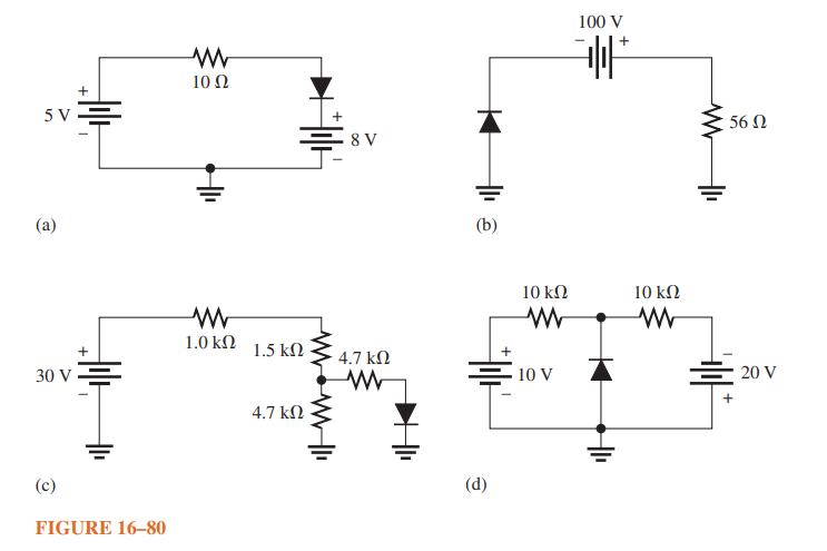
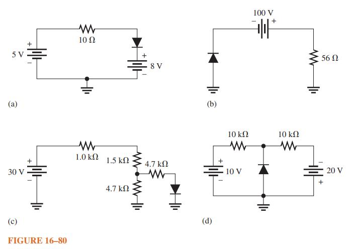
Determine whether each diode in Figure 16–80 is forward-biased or reverse-biased. SV 30 V (c) + Ar + FIGURE 16-80 10 1.0 1.5 4.7 8 V 4.7 (d) 10 10 V 100 V + 10 www 56 + 20 V
What would cause the barrier potential to decrease from 0.7 V to 0.6 V?
Determine the voltage across each diode in Figure 16–80. 5V (2) + (c) 1 + 30 v Ξ FIGURE 16-80 www 10 Ω Μ 1.0 ΚΩ 1.5 ΚΩ 4.7 ΚΩ 8 V · 4.7 ΚΩ Μ (b) (d) 10 ΚΩ Μ Ξ10V 100 V Η HI + 10 ΚΩ Μ 56 Ω 20 V
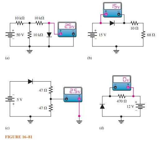
Examine the meter indications in each circuit of Figure 16–81, and determine whether the diode is functioning properly, or whether it is open or shorted. (a) (c) 10 ΚΩ Μ 50 V SV HI HI FIGURE 16-81 10 ΚΩ Μ 10 ΚΩ 47 Ω 47 Ω Μ Μ 35v Ⓡ 25η tur (b) 15 V (d) 15v 41₁ Ov Μ 470
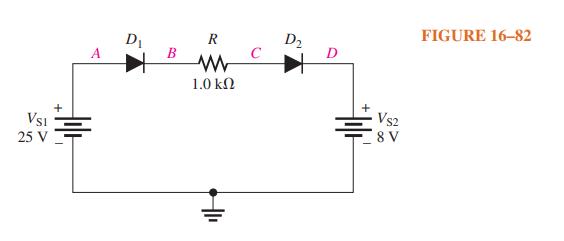
Determine the voltage with respect to ground at each point in Figure 16–82. Vsi 25 V D₁ B R www 1.0 ΚΩ C D₂ VS2 8 V FIGURE 16-82
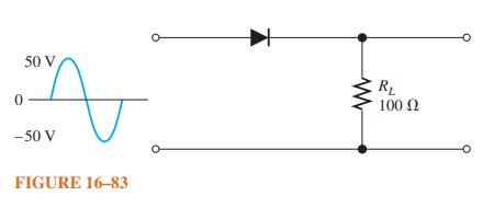
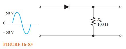
Draw the waveforms for the load current and voltage for Figure 16–83. Show the peak values. 50 V 0 n -50 V FIGURE 16-83 RL 100 Ω
Calculate the average value of a half-wave rectified voltage with a peak value of 200 V.
Can a diode with a PIV rating of 50 V be used in the circuit of Figure 16–83? 50 V 0 -50 V √ FIGURE 16-83 RL 100 Ω
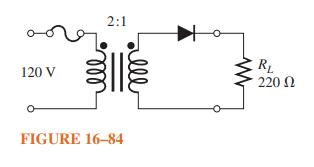
Determine the peak voltage across RL in Figure 16–84. 120 V 2:1 FIGURE 16-84 alll RL 220 Ω
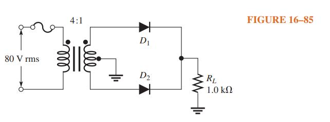
Consider the circuit in Figure 16–85.(a) What type of circuit is this? (b) What is the total peak secondary voltage? (c) Find the peak voltage across each half of the secondary. (d) Draw the voltage waveform across RL. (e) What is the peak current through each diode? (f)
Calculate the average value of a full-wave rectified voltage with a peak value of 75 V.
Calculate the peak voltage rating of each half of a center-tapped transformer used in a full-wave rectifier that has an average output voltage of 110 V.
Show how to connect the diodes in a center-tapped rectifier in order to produce a negative going full-wave voltage across the load resistor.
What PIV rating is required for the diodes in a bridge rectifier that produces an average output voltage of 50 V?
When S2 is at a positive peak, are any of the isolation diodes forward-biased? If so, which?
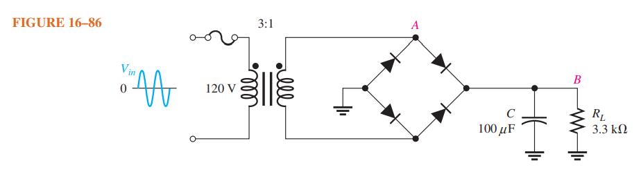
Refer to Figure 16–86 and draw the waveforms VA and VB with relation to the input waveform. FIGURE 16-86 Vin 0 120 V 3:1 A C 100 F B RL 3.3
The ideal dc output voltage of a capacitor-input filter is the (peak, average) value of the rectifi ed input.
A certain voltage regulator has a no-load output voltage of 12.6 V and a full-load output voltage of 12.1 V. Determine the percent load regulation.
A zener diode has a VZ = 7.5 V and a ZZ = 5 Ω. Draw the equivalent circuit.
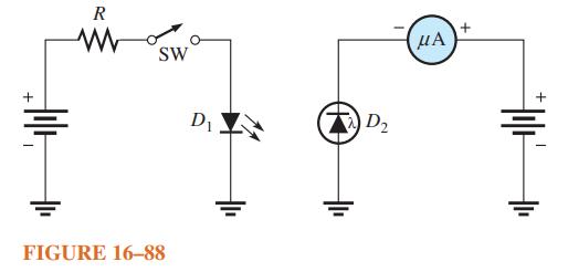
When the switch in Figure 16–88 is closed, will the microammeter reading increase or decrease? Assume that D1 and D2 are optically coupled. + R W SW FIGURE 16-88 D₁ Dy HA + 낳
From the meter readings in Figure 16–89, determine if the rectifi er is functioning properly. If it is not, determine the most likely failure(s). DMM1 is an ac voltmeter; DMM2 and DMM3 are dc voltmeters. 120 V 10:1 мее lll FIGURE 16-89 12 v DMM1 R surge www 10.8v DMM2 C RL Ov DMM3
With no incident light, there is a certain amount of reverse current in a photodiode. What is this current called?
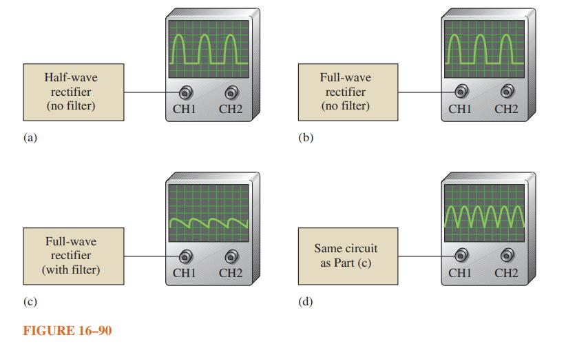
Each part of Figure 16–90 shows oscilloscope displays of rectifier output voltages. In each case, determine whether or not the rectifier is functioning properly and, if it is not, identify the most likely failure(s). (c) Half-wave rectifier (no filter) Full-wave rectifier (with filter) FIGURE
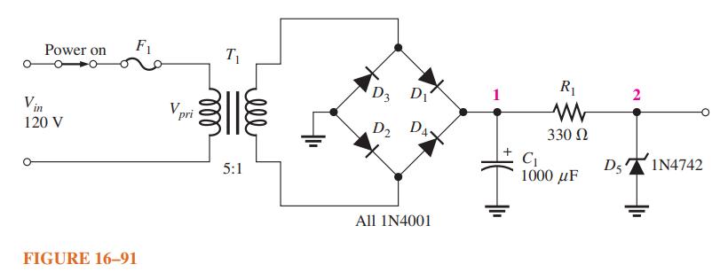
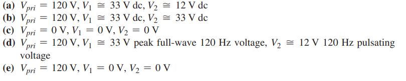
For each set of measured voltages at nodes 1 and 2 indicated in Figure 16–91, determine if they are correct, and if not, identify the most likely fault(s). State what you would do to correct the problem once it is isolated. Power on Vin 120 V F₁ FIGURE 16-91 V
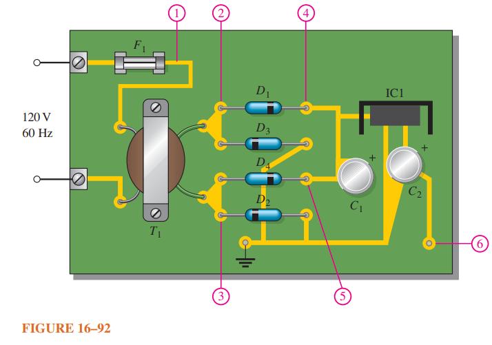
Determine the most likely failure in the circuit board of Figure 16–92 for each of the following symptoms. State the corrective action you would take in each case. The transformer has a turns ratio of 1. (a) No voltage across the primary (b) No voltage at point 2 with respect to ground;
What is the value of IC for IE = 5.34 mA and IB = 475 μA?
In a certain transistor circuit, the base current is 2% of the 30 mA emitter current. Determine the collector current.
Refer to Figure 17–66 and determine the general effect of each of the following failures: ΤΡΙ 100 μV rms 0V de TP2 100 μV rms 1.75 V de C₁ OF 1μF www www R₁ 47 ΚΩ R₂ 10 ΚΩ www TP3 6.85 mV rms 5.07 V de R3 4.7 ΚΩ R₁ 1.0 k C₂ 10μF +10 V S1 HE 1 μF TP4 6.85 mV rms 1.75 V
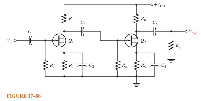
What symptom(s) would indicate each of the following failures under signal conditions in Figure 17–88? Vino C₁ HE FIGURE 17-88 www R3 +9₁ R₁ R₂ C3 S C₂ www R4 R6 B0₂ www R5 -o +VDD C5 R1₁ O V out
Compare a practical op-amp to an ideal op-amp.
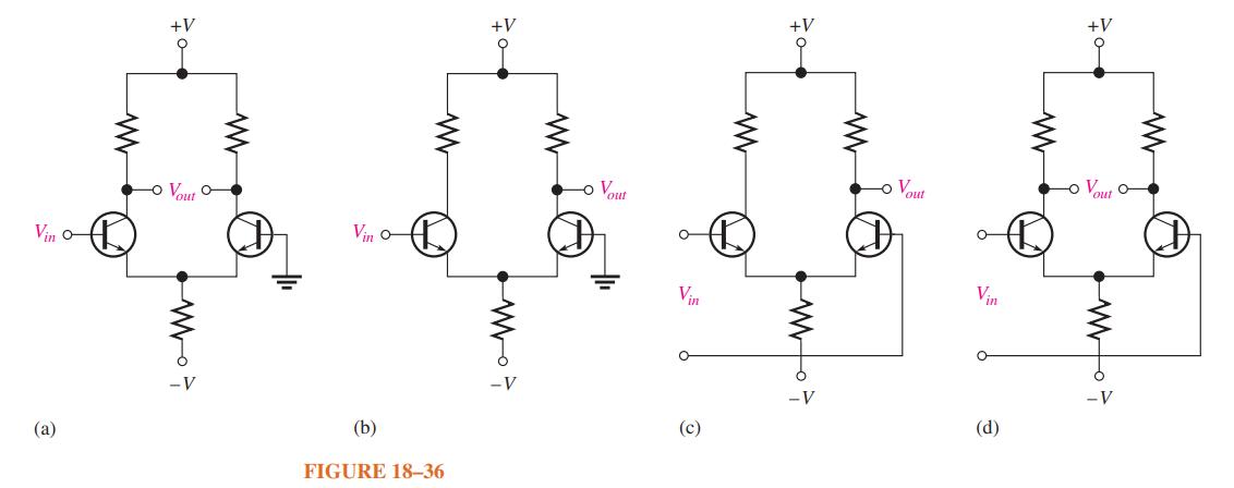
Identify the type of input and output configuration for each diff-amp in Figure 18–36. (a) WWW (b) www FIGURE 18-36 MOT (c) 3 Vin (d) Vout o www -V 1-
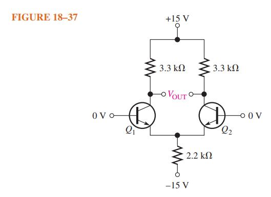
The dc base voltages in Figure 18–37 are zero. Using your knowledge of transistor analysis, determine the dc differential output voltage. Assume that Q1 has an α = 0.98 and Q2 has an α = 0.975. FIGURE 18–37 0 Vo Q₁ +15 V 3.3 ΚΩ το OVOUT O 2.2 ΚΩ –15 V 3.3 ΚΩ Ως 00V
A certain diff-amp has a differential gain of 60 and a common-mode gain of 0.09. Determine the CMRR and express it in decibels.
A certain diff-amp has a CMRR of 65 dB. If the differential gain is 150, what is the common mode gain?
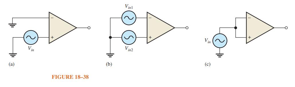
Identify the type of input mode for each op-amp in Figure 18–38. (a) Vin FIGURE 18-38 (b) Vin1 Vin2 Vin
Show the common-mode input in Figure 18–38 in an alternate way. FIGURE 18-38 Vin1 Vin2 Vin
A certain op-amp has a CMRR of 250,000. Convert this to decibels.
The open-loop gain of a certain op-amp is 175,000. Its common-mode gain is 0.18. Determine the CMRR in decibels.
The op-amp data sheet specifies a CMRR of 300,000 and an Aol of 90,000. What is the common mode gain?
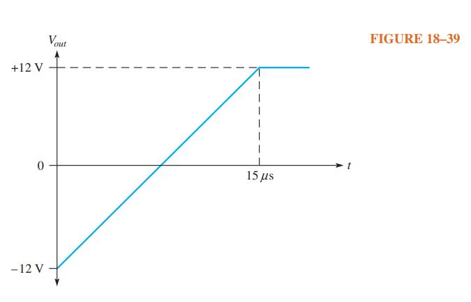
Figure 18–39 shows the output voltage of an op-amp in response to a step input. What is the slew rate? +12 V 0 -12 V Vout 15 us FIGURE 18-39
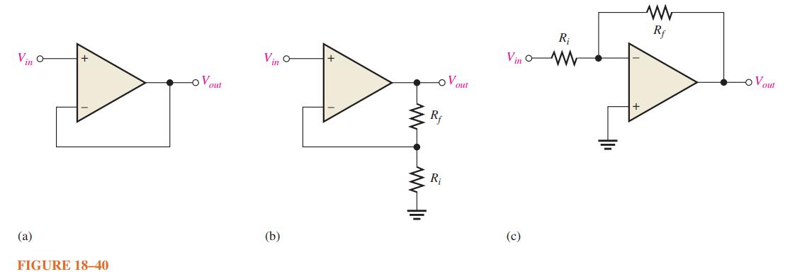
Identify each of the op-amp configurations in Figure 18–40. Vin (a) FIGURE 18-40 V out Vin O- (b) WWII O Rf R₁ V out Vin O- (c) R₁ ww Rf o Vout
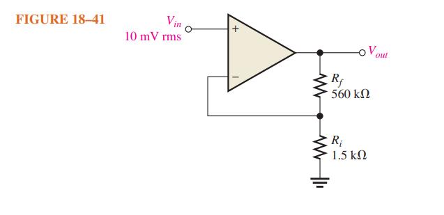
For the amplifier in Figure 18–41, determine the following: (a) Acl(NI) (b) Vout (c) Vf FIGURE 18-41 Vin 10 mV rms www www11 -OV out Rf 560 ΚΩ R₁ 1.5 ΚΩ
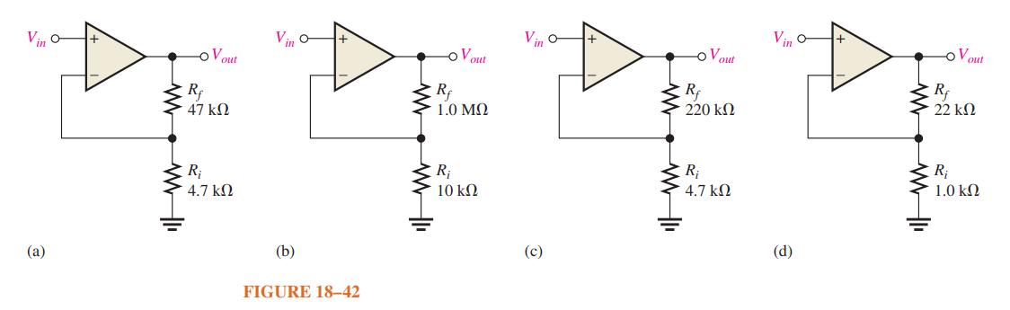
Determine the closed-loop gain of each amplifier in Figure 18–42. Vin o Vino- Vin o OV out -OV out - Vout Rf Rf Rf 47 k2 1.0 MO 220 kO 나나랑 R₁ R₁ R₁ 4.7 k2 10k2 4.7k0 (a) (b) FIGURE 18-42 (c) Vin (d) ww -OV out Rf 22 kO R₁ 1.0 k2
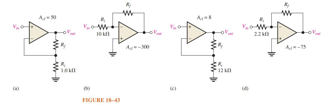
Find the value of Rf that will produce the indicated closed-loop gain in each amplifier in Figure 18–43. Rf Aer = 50 Act = 8 R; Vino- Vino-W Vino- V -o Vout V out out 10 k2 车按车 Rf Rf Ag=-300 R; R₁ 1.0 kQ 12 k (a) (b) FIGURE 18-43 (c) R; Vino-M 2.2 k (d) Rf W Aeg=-75 o Vout
If a signal voltage of 10 mV rms is applied to each amplifier in Figure 18–44, what are the output voltages and what is their phase relationship with inputs? Vino+ (a) FIGURE 18-44 -OV out R Vino-M 100 (b) Rf 100 -OV out Vin o (c) V Vout Rf - 1.0 R 47 Vin R 33 (d) Rf www 330 -O out
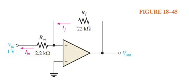
Determine the approximate values for each of the following quantities in Figure 18–45:(a) IIn (b) If (c) Vout (d) Closed-loop gain. in 1V Rin www I 2.2 ΚΩ +₁ Rf 22 ΚΩ Vout FIGURE 18-45
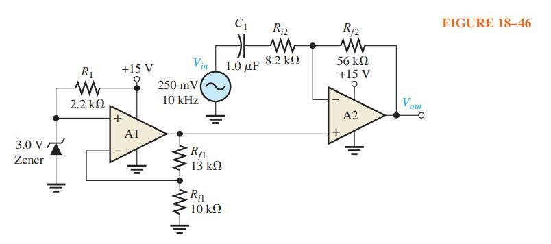
For the single-supply circuit shown in Figure 18–46,(a) What voltage do you expect to see at A2’s noninverting input? (b) What is the gain of A2 to the ac signal? 3.0 V. Zener R₁ Μ 2.2 ΚΩ + +15 V A1 C₁ Η Vin 1.0 μF με 250 mV/ 10 kHz R₁ 13 ΚΩ R₁ 10 ΚΩ Riz 8.2
Refer to Figure 18–46. Given a 10 kHz, 250 mV input signal, sketch the Vout for A2 you would expect to see on an oscilloscope. Draw two cycles and show both the dc and the ac components. 3.0 V Zener R 2.2 + +15 V Al C V | 1.0 F 250 mV/ 10 kHz R 13 R 10 Riz 8.2 R 56 +15 V 2 + Vout FIGURE
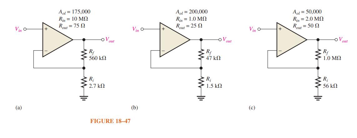
Determine the input and output resistances for each amplifier configuration in Figure 18–47. Aot = 175,000 Aot = 200,000 Aoi = 50,000 Rin = 10 M2 Rin = 1.0 MO R = 2.0 MQ Rout = 75 Q Vin O- + Vin O- R = 25 Q Vin O- R = 50 2 -OV out out OV out Rf 學哔哩 Rf Rf 560 k2 47 kQ 1.0 MO R; R₁ R₁ 2.7
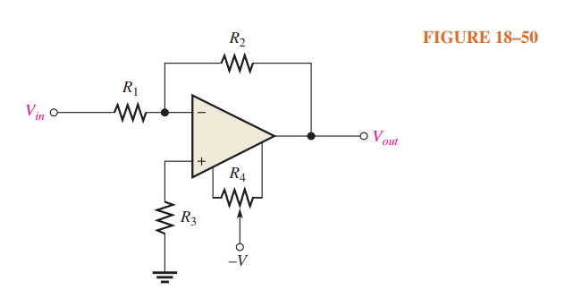
Determine the most likely fault(s) for each of the following symptoms in Figure 18–50 with a 100 mV signal applied. (a) No output signal. (b) Output severely clipped on both positive and negative swings. (c) Clipping on only positive peaks when input signal is increased to a
For the circuit in Figure 15–50, what can account for an output that is nearly equal to the negative power supply voltage? R₁ www WWII + R3 R₂ ww R4 -V Vout FIGURE 18-50
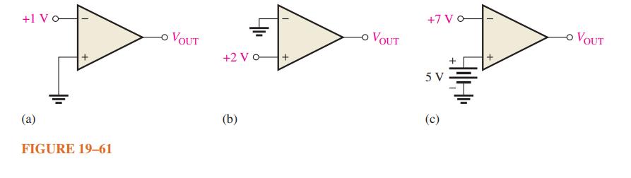
Determine the output level (maximum positive or maximum negative) for each comparator in Figure 19–61. +1 Vo (a) FIGURE 19-61 VOUT +2 Vo (b) VOUT +7 Vo 5 V (c) + VOUT
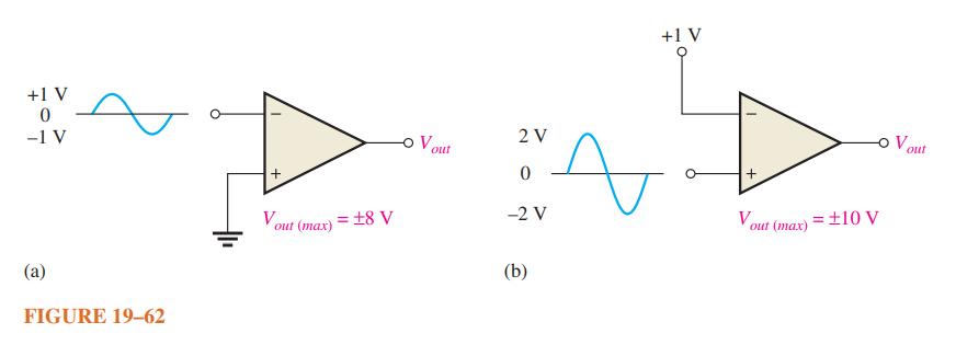
Draw the output voltage waveform for each circuit in Figure 19–62 with respect to the input. Show voltage levels. +1 V 0 -1 V (a) FIGURE 19-62 E Vout (max) + = +8 V Vout 2 V 0 -2 V (b) +1 V t + V out (max) = 10 V Vout
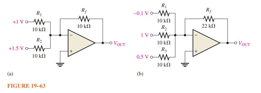
Determine the output voltage for each circuit in Figure 19–63. R₁ +IvoM 10 ΚΩ R₂ +1.5vo M 10 ΚΩ (2) FIGURE 19–63 + Rf 10 ΚΩ O VOUT -0.150M IV R₁ 10 ΚΩ R₂ M 10 ΚΩ R3 0.50Μ 10 ΚΩ (b) + Rf Μ 22 ΚΩ VOUT
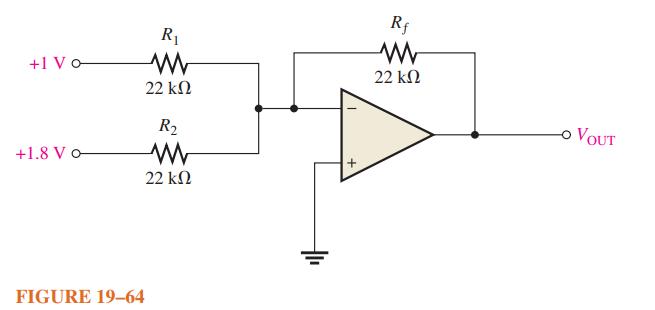
Determine the following in Figure 19–64.(a) VR1 and VR2 (b) current through Rf (c) VOUT. +1Va +1.8 Vo FIGURE 19-64 R₁ Μ 22 ΚΩ R₂ 22 ΚΩ Rf Μ 22 ΚΩ -O VOUT
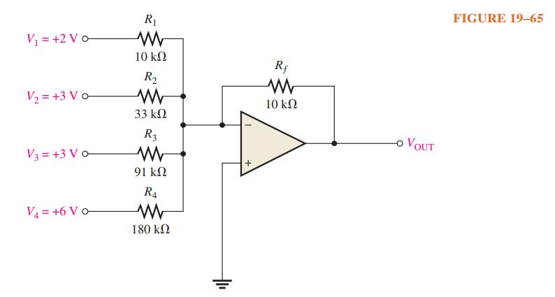
Find the output voltage when the input voltages shown in Figure 19–65 are applied to the scaling adder. What is the current through Rf? V = +2 Vo V = +3 Vo V=+3 Vo V = +6 Vo R₁ Μ 10 ΚΩ R₂ 33 ΚΩ R3 Μ 91 ΚΩ R4 Μ 180 ΚΩ + Rf Μ 10 ΚΩ -O VOUT FIGURE 19-65
Showing 100 - 200
of 641
1
2
3
4
5
6
7
Step by Step Answers