

Question: Find the individual transistor widths k and k for the Driver to achieve nMOS PMOS the worst-case effective rise and fall resistance equal to
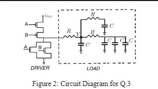
Find the individual transistor widths k and k for the Driver to achieve nMOS PMOS the worst-case effective rise and fall resistance equal to that of a unit inverter, R. Draw the simplified RC circuit for Figure 2. 1) Derive the expressions for tand t for node Y. . pdr ii) Calculate t and t, in s (second) from the simplified RC expression from pdf par (1) when R= 1 kQ and C= 2 pF. Veo DRIVER R C R LOAD Figure 2: Circuit Diagram for Q.3
Step by Step Solution
3.38 Rating (154 Votes )
There are 3 Steps involved in it
Answer Recall that a 2input NOR gate has the following transistor level schematic Figure 1 Transisto... View full answer

Get step-by-step solutions from verified subject matter experts