

Question: MIPS multi-cycled CPU (datapath & control) simulation Write a simulation code for the multi-cycled implementation of the MIPS architecture. The multi-cycled datapath with control signals
MIPS multi-cycled CPU (datapath & control) simulation
Write a simulation code for the multi-cycled implementation of the MIPS architecture.
The multi-cycled datapath with control signals is illustrated in Figure 5.28 (attached) and
micro operations of each cycle are shown in Figure 5.30 (attached).
The datapath uses only one ALU since multiple execution steps for an instruction share it
in different clock cycles. You should use the 32-bit ALU simulation module, which was
built in the phase 1.
In each clock cycle, appropriate control signals are generated to control needed components
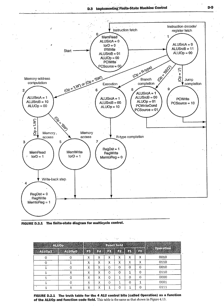
in the datapath. You should use the FSM-based control a state diagram of the FSM is
shown in Figure D.3.1 (attached).
Major components in the simulation
Memory: Memory consists of both instructions and data. In the simulation, use a
simplified memory module that starts from byte address 0hex and ends with
byte address C7hex (199dec). Assume that the instruction starts from byte
address 0hex and the data starts from byte address 64hex (100dec).
Register file: There are 32 registers in the register file.
In the simulation code, you should prepare a table with two fields, i.e.,
register_number and 32-bit content.
32-bit ALU: the one you designed in Phase 1; it should handle 6 operations
(AND, OR, Add, Sub, Slt, NOR) and also generate Zero and Overflow output (1/0).
Special/Intermediate Registers: each 32-bits long
PC (Program Counter)
IR (Instruction Rgister)
MDR (Memory Data Register): for load instruction
A: operand1 for ALU
B: operand2 for ALU
ALUout: result from ALU
Other Components:
Mux-1: Selects memory address for instruction (PC) or data (ALUout), based on
control signal IorD.
Mux-2: Selects write-register number from rt (for load) and rd (for R-type), based on
the control signal RegDst.
Mux-3: Selects Write-data from ALUout (for R-type) and MDR (for load), based on
the control signal MemtoReg.
Mux-4: Selects ALU operand-1 from PC and A, based on the control signal ALUSrcA.
Mux-5: Selects ALU operand-2 from B, #4 (for PC+4), sign-extended offset (for load/store),
sign-extended&
Mux-6: Selects the next PC value from ALU (PC+4), ALUout (branch target), and
Jump target, based on the 2-bit control signal PCSource.
Sign-extend unit: converts 16-bit number to 32-bit sign-extended number.
Shift-left2 unit: performs
Control Unit
In each clock cycle, the control unit (you should write a simulation module) generates
appropriate control signals and components in the datapath operate based on them.
Instruction Set
Your simulator should handle at least the following subset of MIPS instructions (see lecture note):
Arithmetic: add, sub
Data transfer: lw, sw
Logical: and, or, nor
Conditional branch: beq, bne, slt
Jump: j
-----------------------------------------------------------------------------------------------------------------
Input:
MIPS machine instructions and data for a program is stored in a text file.
Load the instructions into the instruction memory area (starting from byte address 0hex),
and data (if any) into the data memory area (starting from byte address 64hex).
Output:
1. Display the initial configuration; i.e., memory contents with address (0hex ~ C7hex),
and the register file contents (reg. #s and contents)
2. For each clock cycle, display contents of the following intermediate registers;
PC, IR, MDR, A, B, ALUout. //display in binary (32 bits) format
3. Display the final configuration; i.e., memory contents with address (0hex ~ C7hex)
and the register file contents (reg. # and contents).
Simulation project sample testing code
Assumptions: initial value of $gp = 64hex (100dec)
value of $zero = 0
Sample high-level code:
load x;
load y;
while (x
y = y-1;
store y;
Corresponding MIPS assembly code:
lw $t0, 0($gp); x
lw $t1, 4($gp); y
lw $s0, 8($gp); #1
Loop: slt $s1, $t0, $t1; if (t0
beq $s1, $zero, Exit; if s1 ==0, Exit
sub $t1, $t1, $s0; y = y - 1
j Loop;
Exit: sw $t1, 4($gp); store y
Loader format:
8 3
10001111100010000000000000000000
10001111100010010000000000000100
10001111100100000000000000001000
00000001000010011000100000101010
00010010001000000000000000000010
00000001001100000100100000100010
00001000000000000000000000000011
10101111100010010000000000000100
00000000000000000000000000000011
00000000000000000000000000000101
00000000000000000000000000000001
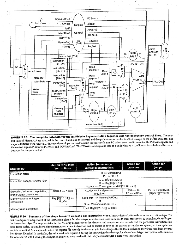
PCSource ALUOp ALUSrcB ALUSrcA PCWriteCond PCWrite MemReadControl MemWrile Op RegWrite IRWrite Shift28 left 2 address [31-0] 26 Instruction 125-01 Instruction 31-26] Instruction (25-21] PC (31-28] register 1 Read data 1 ero Memory MemData (20-16] ALU ALU Registers MWrite xregister data 2 15-0Instruction U Read [15-11 Write data Instruction Write ut register Instruction [15-0 32 /shift eft 2 ALU control Memory 16 Sign register Instruction [5-0 plete datapath for the multicycle impiomentation together with the necessary. control lines. The con- lines of Figure 5.27 are attached to the control unit, and the control and datapath elements needed to effect changes to the Pare included. The r additions from Figure 527 include the multiplexor used to select the source of a new P value, gates used to combine the PCwrite sgnals and FIGURE 5.28 The com PCWrite, and PCWriteCond. The PCWriteCond signal is used to decide whether a conditional branch should be taken. the control signals PCSource, Support for jumps is included. Action for R-lype instructions Action for memory- reference instructions Action for branches Action for jumns Step naine Instruction fetch Instruction decode/register fetch IR = Memory(PC) A Rg IA 25:21)l ALUOutPC(sign-extend (R15:0)
Step by Step Solution
There are 3 Steps involved in it

Get step-by-step solutions from verified subject matter experts