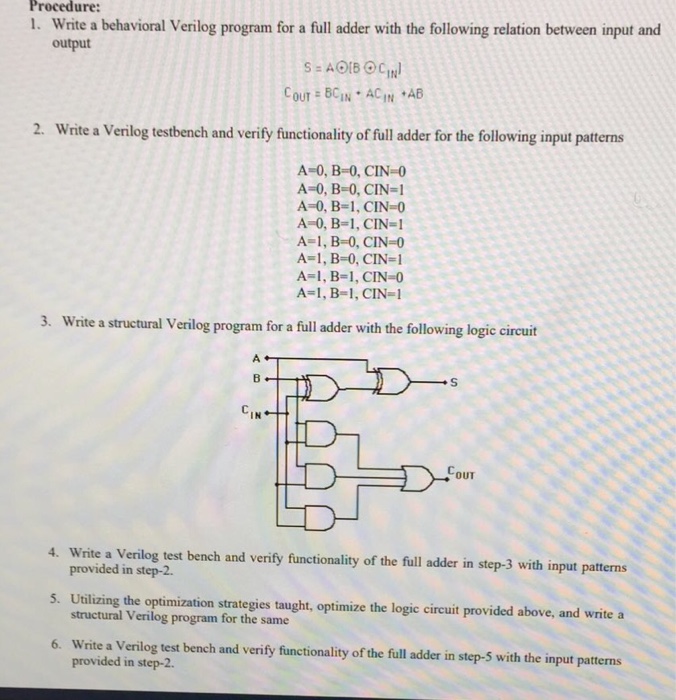
Question: Procedure: 1. Write a behavioral Verilog program for a full adder with the following relation between input and output 2. Write a Verilog testbench and


Procedure: 1. Write a behavioral Verilog program for a full adder with the following relation between input and output 2. Write a Verilog testbench and verify functionality of full adder for the following input patterns A-0, B-0, CIN-0 A-0, B-0, CIN-1 A-0, B-1, CIN-0 A-0, B-I, CIN=1 A-1, B-0, CIN-0 A=1, B-0, CIN=1 A-1, B=I, CIN-0 A-1, B-1, CIN-1 3. Write a structural Verilog program for a fulladder with the following logic circuit D IN OUT 4. Write a Verilog test bench and verify functionality of the full adder in step-3 with input patterns 5. Utilizing the optimization strategies taught, optimize the logic circuit provided above, and write a 6. Write a Verilog test bench and verify functionality of the full adder in step-5 with the input patterns provided in step-2. structural Verilog program for the same provided in step-2. Procedure: 1. Write a behavioral Verilog program for a full adder with the following relation between input and output 2. Write a Verilog testbench and verify functionality of full adder for the following input patterns A-0, B-0, CIN-0 A-0, B-0, CIN-1 A-0, B-1, CIN-0 A-0, B-I, CIN=1 A-1, B-0, CIN-0 A=1, B-0, CIN=1 A-1, B=I, CIN-0 A-1, B-1, CIN-1 3. Write a structural Verilog program for a fulladder with the following logic circuit D IN OUT 4. Write a Verilog test bench and verify functionality of the full adder in step-3 with input patterns 5. Utilizing the optimization strategies taught, optimize the logic circuit provided above, and write a 6. Write a Verilog test bench and verify functionality of the full adder in step-5 with the input patterns provided in step-2. structural Verilog program for the same provided in step-2
Step by Step Solution
There are 3 Steps involved in it

Get step-by-step solutions from verified subject matter experts


