

Question: What is the clock cycle time with and without this improvement? When processor designers consider a possible improvement to the processor datapath, the decision usually
What is the clock cycle time with and without this improvement?
When processor designers consider a possible improvement to the processor datapath, the decision usually depends on the cost/performance trade-off. In the following three problems, assume that we are starting with a datapath from Figure 4.2, where I-Mem, Add, Mux, ALU, Regs, D-Mem, and Control blocks have latencies of 400ps, 100ps, 30ps, 120ps, 200ps, 350ps, and 100ps, respectively, and costs of 1000, 30, 10, 100, 200, 2000, and 500, respectively. The remaining three problems in this exercise refer to the following processor improvement: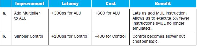
Figure 4.2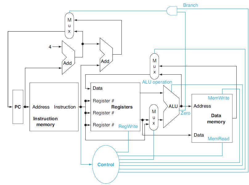
a. b. Improvement Add Multiplier to ALU Simpler Control Latency +300ps for ALU +100ps for Control Cost +600 for ALU -400 for Control Benefit Lets us add MUL instruction. Allows us to execute 5% fewer instructions (MUL no longer emulated). Control becomes slower but cheaper logic.
Step by Step Solution
3.44 Rating (163 Votes )
There are 3 Steps involved in it
To analyze the impact of the proposed improvement on the clock cycle time lets compare the clock cyc... View full answer

Get step-by-step solutions from verified subject matter experts