

Question: For the given figure: 1. Write the Verilog HDL code of the circuit in the figure 2. Draw the Project Design using schematic circuit diagram
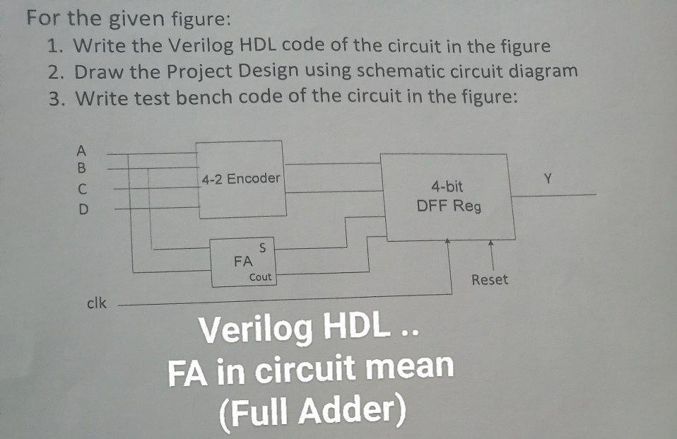
For the given figure: 1. Write the Verilog HDL code of the circuit in the figure 2. Draw the Project Design using schematic circuit diagram 3. Write test bench code of the circuit in the figure: A B 4-2 Encoder Y C D 4-bit DFF Reg S FA Cout Reset clk Verilog HDL.. FA in circuit mean (Full Adder)
Step by Step Solution
There are 3 Steps involved in it
1 Expert Approved Answer
Step: 1 Unlock

Question Has Been Solved by an Expert!
Get step-by-step solutions from verified subject matter experts
Step: 2 Unlock
Step: 3 Unlock