

Question: IV. A: write the Verilog code for a 12-bit shift register with ability to shift left or right, synchronized parallel load, asynchronous reset, and serial
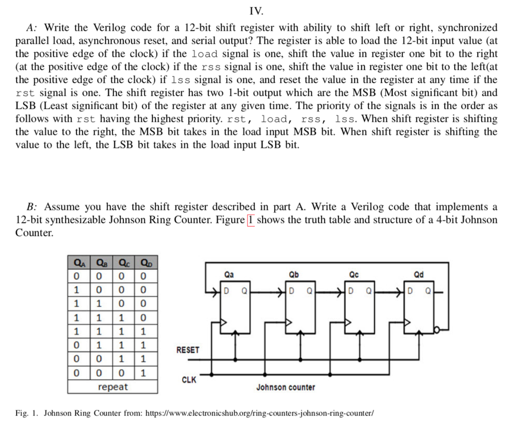
IV. A: write the Verilog code for a 12-bit shift register with ability to shift left or right, synchronized parallel load, asynchronous reset, and serial output? The register is able to load the 12-bit input value (at the positive edge of the clock) if the load signal is one, shift the value in register one bit to the right (at the positive edge of the clock) if the rss signal is one, shift the value in register one bit to the left(at the positive edge of the clock) if lss signal is one, and reset the value in the register at any time if the rst signal is one. The shift register has two 1-bit output which are the MSB (Most significant bit) and LSB (Least significant bit) of the register at any given time. The priority of the signals is in the order as follows with rst having the highest priority. rst, load, rss, lss. When shift register is shifting the value to the right, the MSB bit takes in the load input MSB bit. When shift register is shifting the value to the left, the LSB bit takes in the load input LSB bit. B: Assume you have the shift register described in part A. Write a Verilog code that implements a 12-bit synthesizable Johnson Ring Counter. Figure I shows the truth table and structure of a 4-bit Johnson Counter. Qb Qc Qd 1 00 0 D Q D Q D Q D Q 1 1 1 0 0 1 1 1 0 0 1 1 0 0 0 1 RESET CLK repeat Johnson counter Fig. 1. Johnson Ring Counter from: https://www.electronicshub.org/ring-counters-johnson-ring-counter/
Step by Step Solution
There are 3 Steps involved in it

Get step-by-step solutions from verified subject matter experts