

Question: Write a VHDL testbench to test all combinations of inputs to the full adder Exercise 3.5. Verify the correctness of your full adder and of
Write a VHDL testbench to test all combinations of inputs to the full adder Exercise 3.5. Verify the correctness of your full adder and of the testbench using a VHDL simulator.
Data From Exercise 3.5:
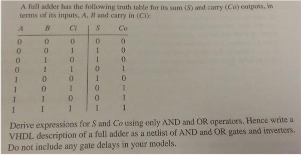
A full adder has the following truth table for its sum (S) and carry (Co) outputs, in terms of its inputs, A, B and carry in (Ci): Ci Co 1. 0. 0. Derive expressions for S and Co using only AND and OR operators. Hence write a VHDL description of a full adder as a netlist of AND and OR gates and inverters. Do not include any gate delays in your models.
Step by Step Solution
3.50 Rating (153 Votes )
There are 3 Steps involved in it
To create a VHDL testbench for the full adder described in Exercise 35 ... View full answer

Get step-by-step solutions from verified subject matter experts