New Semester
Started
Get
50% OFF
Study Help!
--h --m --s
Claim Now
Question Answers
Textbooks
Find textbooks, questions and answers
Oops, something went wrong!
Change your search query and then try again
S
Books
FREE
Study Help
Expert Questions
Accounting
General Management
Mathematics
Finance
Organizational Behaviour
Law
Physics
Operating System
Management Leadership
Sociology
Programming
Marketing
Database
Computer Network
Economics
Textbooks Solutions
Accounting
Managerial Accounting
Management Leadership
Cost Accounting
Statistics
Business Law
Corporate Finance
Finance
Economics
Auditing
Tutors
Online Tutors
Find a Tutor
Hire a Tutor
Become a Tutor
AI Tutor
AI Study Planner
NEW
Sell Books
Search
Search
Sign In
Register
study help
engineering
digital design using vhdl a systems approach
Digital Design Using VHDL A Systems Approach 1st Edition William J. Dally, R. Curtis Harting, Tor M. Aamodt - Solutions
Convert 2015 from unsigned hexadecimal to decimal notation. Also express the number in binary-coded decimal (BCD) notation.
Using full adders, design a circuit that accepts a seven-bit input and outputs the number of inputs that are 1 as a three-bit binary number.
Design a circuit that accepts two sign-magnitude binary numbers and outputs their sum, also in sign-magnitude form.
Using adders, combinational building blocks, and gates, design a circuit that accepts a four-bit 2’s complement binary input a(3 downto 0) and outputs a seven-bit 2’s complement output b(6 downto 0) that is five times the value input. You cannot use a multiplier building block. Use the minimum
Divide the following pair of unsigned binary numbers (show each step of the process): 1011102 ÷ 0112.
Divide the following pair of unsigned hexadecimal numbers (show each step of the process): F716 ÷ 616.
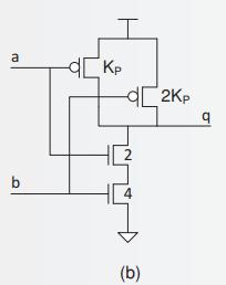
Compute the maximum and minimum rise/fall times of the gates shown in Figure 5.18(b). Assume that only one input toggles at a time and that the gates drive an output of 4Cinv. You may leave your answer in terms of tinv.Data in Figure 5.18(b). a b Kp -d2Kp 2 4 (b) q
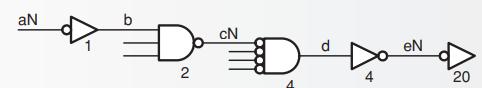
Calculate the delay of the circuit in Figure 5.20 in terms of tinv.Data in Figure 5.20 aN 2 cN P eN 20
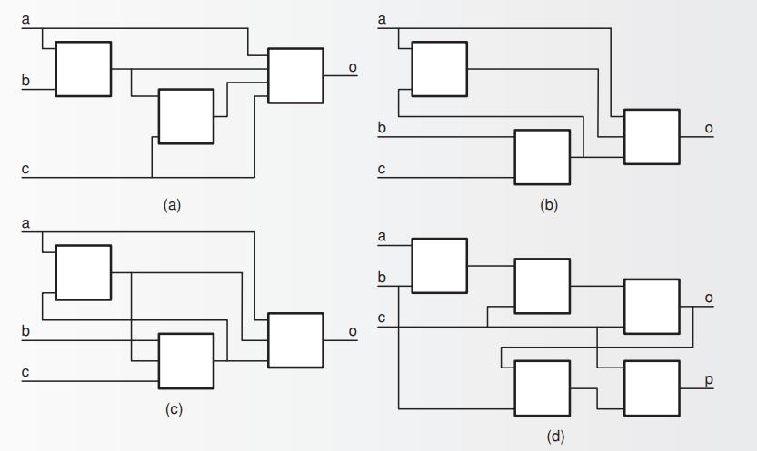
Which of the circuits in Figure 6.23 are combinational? Each of the boxes is itself a combinational circuit. Data in Figure 6.23 a b с a b с (a) (c) a b C a b O (b) (d) I Р
Calculate the delay of the circuit in Figure 5.21 in terms of tinv.Data in Figure 5.21 a bN C 3 fo dN 8 e 32
Compute the delay and energy of driving an inverter of size 256 from a minimum-size inverter (size 1) with a series of FO4 inverters. Express your answer in terms of tinv and Einv.
Calculate the delay of a 1 mm wire in 28 nm technology that is divided into five 200 μm segments with a 10 × minimum-size inverter driving each segment.
Design a sum-of-products circuit for segment 1 of the full seven-segment decoder described in Exercise 6.14. Data in Exercise 6.14.This and following exercises (6.14 – 6.41) share the description of a seven-segment decoder, a combinational circuit with a four-bit input a and a seven-bit
How does designing for power differ between a cellular phone radio chip and a high-utilization server processor? What power reduction mechanisms would you use for each? What are the differing constraints?
Design a sum-of-products circuit for segment 3 of the full seven-segment decoder described in Exercise 6.14. Data in Exercise 6.14.This and following exercises (6.14 – 6.41) share the description of a seven-segment decoder, a combinational circuit with a four-bit input a and a seven-bit
Design a four-bit Fibonacci circuit. This circuit outputs a 1 iff its input is a Fibonacci number (i.e., 0, 1, 2, 3, 5, 8, or 13). Go through the following steps. (a) Write a truth table for the function. (b) Draw a Karnaugh map of the function. (c) Identify the prime implicants of
Design a sum-of-products circuit for segment 4 of the full seven-segment decoder described in Exercise 6.14. Data in Exercise 6.14.This and following exercises (6.14 – 6.41) share the description of a seven-segment decoder, a combinational circuit with a four-bit input a and a seven-bit
Design a circuit whose output is true if its four-bit input is really a prime number – not including “1” – that is, the output is true if the input is 2, 3, 5, 7, 11, or 13. Go through the same steps as in Exercise 6.2. Data in Exercise 6.2.Design a four-bit Fibonacci circuit. This
Design a sum-of-products circuit for segment 5 of the full seven-segment decoder described in Exercise 6.14. Data in Exercise 6.14.This and following exercises (6.14 – 6.41) share the description of a seven-segment decoder, a combinational circuit with a four-bit input a and a seven-bit
Design a circuit whose output is true if its four-bit decimal input is really a prime number – not including “1” – that is, the output is true if the input is 2, 3, 5 or 7. The output is an X (don’t care) for input combinations 10–15. Go through the same steps as in Exercise
Design a sum-of-products circuit for segment 6 of the full seven-segment decoder described in Exercise 6.14. Data in Exercise 6.14. This and following exercises (6.14 – 6.41) share the description of a seven-segment decoder, a combinational circuit with a four-bit input a and a
Design a sum-of-products circuit for segment 2 of the full seven-segment decoder described in Exercise 6.14. Data in Exercise 6.14.This and following exercises (6.14 – 6.41) share the description of a seven-segment decoder, a combinational circuit with a four-bit input a and a seven-bit
Design a four-input multiple-of-3 circuit, that is a circuit whose output is true if the input is 3, 6, 9, 12, or 15.
Design a five-input prime number circuit. The output is true if the input is a prime number (not including “1”) between 0 and 31.
Design a sum-of-products circuit for segment 1 of the decimal seven-segment decoder described in Exercise 6.14. Data in Exercise 6.14.This and following exercises (6.14 – 6.41) share the description of a seven-segment decoder, a combinational circuit with a four-bit input a and a seven-bit
Design a six-input prime number circuit. This circuit must also recognize the primes between 32 and 63 (neither of which is prime).
Design a sum-of-products circuit for segment 2 of the decimal seven-segment decoder described in Exercise 6.14. Data in Exercise 6.14.This and following exercises (6.14 – 6.41) share the description of a seven-segment decoder, a combinational circuit with a four-bit input a and a seven-bit
Design the decimal Fibonnaci circuit of Exercise 6.4 in product-of sums form.Data in Exercise 6.4Repeat Exercise 6.2, but for a decimal Fibonacci circuit. This circuit need only produce an output for inputs in the range 0–9. The output is a don’t care for the other six input states.
Design the decimal prime number circuit of Exercise 6.6 in product of-sums form.Data in Exercise 6.6 Design a circuit whose output is true if its four-bit decimal input is really a prime number – not including “1” – that is, the output is true if the input is 2, 3, 5 or 7. The output
Design a sum-of-products circuit for segment 0 of the decimal seven-segment decoder described in Exercise 6.14. Data in Exercise 6.14.This and following exercises (6.14 – 6.41) share the description of a seven-segment decoder, a combinational circuit with a four-bit input a and a seven-bit
Design a sum-of-products circuit for segment 3 of the decimal seven-segment decoder described in Exercise 6.14. Data in Exercise 6.14.This and following exercises (6.14 – 6.41) share the description of a seven-segment decoder, a combinational circuit with a four-bit input a and a seven-bit
Design a sum-of-products circuit for segment 4 of the decimal seven-segment decoder described in Exercise 6.14.Data in Exercise 6.14.This and following exercises (6.14 – 6.41) share the description of a seven-segment decoder, a combinational circuit with a four-bit input a and a seven-bit output
Design a sum-of-products circuit for segment 6 of the decimal seven-segment decoder described in Exercise 6.14.Data in Exercise 6.14.This and following exercises (6.14 – 6.41) share the description of a seven-segment decoder, a combinational circuit with a four-bit input a and a seven-bit output
Design a sum-of-products circuit for segment 5 of the decimal seven-segment decoder described in Exercise 6.14. Data in Exercise 6.14.This and following exercises (6.14 – 6.41) share the description of a seven-segment decoder, a combinational circuit with a four-bit input a and a seven-bit
Fix the hazard that may occur in Figure 6.24(a).Dats in Figure 6.24(a). a b C (a)
Fix the hazard that may occur in Figure 6.24(b).Data in Figure 6.24(b). a b C D (b)
Write a VHDL description for a circuit that accepts a four-bit input and outputs true if the input is a Fibonacci number (0, 1, 2, 3, 5, 8, or 13). Your implementation must be done via a concurrent assignment statement using a minimized logic function.
Write a testbench and verify that your design entities from Exercises 7.1–7.3 all work correctly. Which of the four design entities did you find easiest to write and maintain?Data in Exercises 7.1Write a VHDL description for a circuit that accepts a four-bit input and outputs true if the input is
Use a synthesis tool to synthesize the Fibonacci circuits you wrote in Exercises 7.1–7.3. Draw the resulting logic diagram for each synthesis outputs circuit. Compare and contrast the output circuits from each design entity. Data in Exercises 7.1Write a VHDL description for a circuit that
Write a VHDL description for a circuit that accepts a four-bit input and outputs true if the input is a multiple of 3 (3, 6, 9, 12, or 15). Describe why the approach you chose (case, concurrent assignment, structural) is the right approach.
Write a VHDL test bench for the multiple-of-3 circuit of Exercise 7.7.Data in Exercise 7.7.Write a VHDL description for a circuit that accepts a four-bit input and outputs true if the input is a multiple of 3 (3, 6, 9, 12, or 15). Describe why the approach you chose (case, concurrent assignment,
Write a VHDL description for a circuit that outputs true if its five-bit input is a multiple of 5.
Write a VHDL description for a circuit that outputs true if its eight-bit input is a square number, i.e., 1, 4, 9, ...
Write a VHDL description for a circuit that outputs true if its eight-bit input is a cube, i.e., 1, 8, 27, 64, ...
Write a VHDL design entity that takes a five-bit input, input, and outputs a five-bit value that is equal to the input with its bits reversed. For example, input 01100 gives output 00110, and input 11110 gives output 01111. You must implement your design entity using a case statement.
Write a VHDL description for a circuit that takes a four-bit input input and produces outputs two, three, five, seven, eleven, and thirteen. A given output is high if the number corresponding to the output evenly divides the input. For example, when the input is 6, outputs two and three are high
Write a structural VHDL description of a 3 → 8 decoder.
Implement a seven-segment decoder using a 4 → 16 decoder and OR gates.
Write a VHDL design entity that implements a 5 → 32 decoder using a 2 → 4 and a 3 → 8 decoder as building blocks.
Write a VHDL design entity that implements a 6 → 64 decoder using 3 → 8 decoders as building blocks.
Write a VHDL design entity that implements a 6 → 64 decoder using 2 → 4 decoders as building blocks.
Implement a large (32-input) multiplexer in which each multiplexer input and its associated select signal is in a different part of a large chip. The 32 inputs and selects are located along a 0.4 mm long line. Show how this can be implemented using static CMOS gates (e.g., NANDs, NORs, and
Implement a four-bit Fibonacci circuit (output true if the input is a Fibonacci number) using an 8 → 1 binary-select multiplexer.
Write a testbench for a 4 → 16 decoder using an encoder as a checker.
Write a VHDL design entity for a priority encoder with programmable priority – an input (one-hot) selects which bit is highest priority. The priority rotates rightward from that bit position.
Write a VHDL design entity for an arbiter with programmable priority – a binary input selects which bit is highest priority. The priority rotates rightward from that bit position.
Design an arbiter when the highest-priority input in each cycle is one input to the right (cyclically) of the input that last won an arbitration. Assume that the previous winner is an input to your module.
Write a VHDL design entity for a three-way magnitude comparator that outputs true if its three inputs are in strict order: a > b > c.
Write a VHDL design entity for a three-way magnitude comparator that outputs true if its three inputs are not out of order: a ≥ b ≥ c.
Design a combinational circuit with three eight-bit inputs that outputs the minimum value of the three.
Implement the four-bit prime number function using a ROM. How large a ROM is needed (what are N and b)? What is stored in each location?
Implement a seven-segment decoder with a ROM. How large a ROM is needed (what are N and b)? What is stored in each location?
Implement the four-bit prime number function using a PLA. How many product terms and sum terms are needed? What are the connections for each term?
Implement a seven-segment decoder with a PLA. How many product terms and sum terms are needed? What are the connections for each term?
Using combinational building blocks such as adders, comparators, multiplexers, decoders, encoders, and arbiters, as well as logic gates, design a circuit that accepts five three-bit one-hot numbers and outputs the three-bit one-hot number that occurred most often on the inputs. Ties can be broken
Code your design from Exercise 9.3 in VHDL and exhaustively verify it with a testbench. Data in Exercise 9.3Using an approach similar to the multiple-of-3 circuit of Section 9.1, design a multiple-of-5 circuit that outputs true iff its eight-bit input is a multiple of 5.
Design a circuit that outputs true if its eight-bit input is a multiple of 10.
Code your design from Exercise 9.5 in VHDL and exhaustively verify it with a testbench.Data in Exercise 9.5Design a circuit that outputs true if its eight-bit input is a multiple of 10.
Recode the NextDayOfWeek design entity so it will work with arbitrary definitions of the constants ‘SUNDAY, ‘MONDAY, ..., ‘SATURDAY.
Modify the calendar circuit to work correctly in leap years. Assume your input includes the year – in 12-bit binary format.
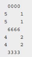
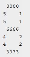
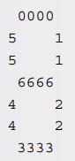
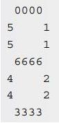
Design a combinational logic circuit that takes a date as the number of days since January 1, 0000, and returns the date in month, day-of-month format.
Prove that the idempotence property is true by using perfect induction.
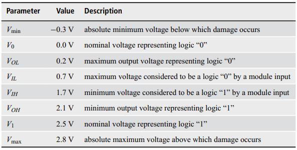
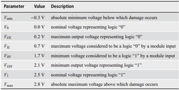
Two wires have been placed close together on a chip. They are so close, in fact, that the larger wire (the aggressor) couples to the smaller wire (the victim) and causes the voltage on the victim wire to change. Using the data from Table 1.1, determine the following. , determine the
Suppose you have a module that uses the encoding described in Table 1.1 but you have freedom to choose either (VOL, VOH) = (0.3, 2.2) or (VOL, VOH) = (0.1, 2.1). Which of these output ranges would you choose and why?Data in Table 1.1 Parameter Value
Two systems, A and B, use the encoding of Table 1.1 to send logic signals to one another. Suppose there is a voltage shift between the two systems’ power supplies so that all voltages in A are VN higher than in B. A voltage of Vx in system A appears as a voltage of Vx + VN in system B. A voltage
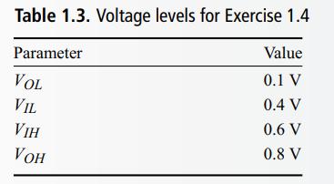
A logic family has signal levels as shown in Table 1.3. We connect device A’s output to B’s inputs using this logic family. All signal levels are relative to the local ground. How much can the ground voltages of the two devices (GNDA and GNDB) differ before an error occurs? Compute the
What is the minimum absolute value of gain for a circuit that restores signals according to the values in Table 1.1? Data in Table 1.1 Parameter Vmin Vo VOL VIL VIH VOH V₁ Vmax Value -0.3 V 0.0 V 0.2 V 0.7 V 1.7 V 2.1 V 2.5 V 2.8 V Description absolute minimum voltage below which damage
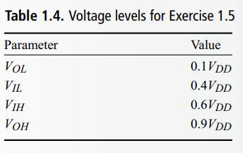
Proportional signal levels. A logic device encodes signals with levels proportional to its power supply voltage (VDD) according to Table 1.4.Suppose two such logic devices A and B send signals to one another and the supply of device A is VDDA = 1.0 V. Assuming that there are no other noise sources
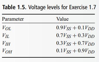
A logic family uses signal levels relative to VSS and proportional to VDD as shown in Table 1.5. We connect two logic devices A and B using this logic family with signals traveling in both directions between the two devices. Both systems have VDD = 1 V, and system A has VSSA = 0 V. Over what range
Suggest a binary representation for playing cards – a set of binary signals that uniquely identifies one of the 52 cards in a standard deck. What different representations might be used to (i) Optimize the density (the minimum number of bits per card) (ii) Simplify operations such as
Derive a representation for colors that supports the operation of additive composition of primary colors. You start with black and add colored light that is red, green, or blue.
Extend the representation of Exercise 1.13 to support three levels of intensity for each of the primary colored lights; that is, each color can be off, weakly on, medium on, or strongly on.Data in Exercise 1.13Derive a representation for colors that supports the operation of additive composition of
A four-core chip is arranged as a 4 × 1 array of processors, where each processor is connected to its east and west neighbors. There are no connections on the ends of the array. The processors’ addresses start at 0 on the east most processor and go up by 1 to address 3 at the west-most
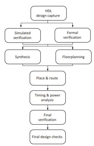
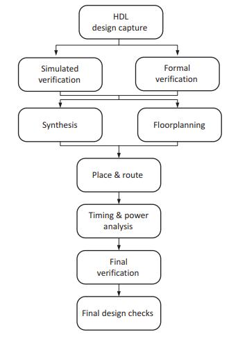
Pick two functions from Figure 2.4, and find and describe three different computer programs that perform each function. Are any of them free? To get you started, leading design vendors include Synopsys and Cadence. Data in Figure 2.4 Simulated verification Synthesis HDL design capture Place &
Come up with a way of encoding the numbers 0–5 onto a four bit binary signal so that adjacent numbers differ in only one bit and also so that the representations of 0 and 5 differ in only one bit.
Congratulations, your video game console from Exercise 2.1 has become a great success! Provide a specification for version 2 of the console. Focus specifically on the changes from version 1, such as whether you will support backwards compatibility.Data in Exercise 2.1You have decided to build an
Give a specification for a traffic-light system to be placed at a busy intersection. Points to consider include how many lights, turn lanes, pedestrians, and light duration. You can assume that traffic is equally heavy in all directions.
You have decided to build an economical (cheap) video game system. Provide a specification of your design. Include components, inputs and outputs, and device media.
Provide a buy vs. build decision and rationale for three of the components from the video game system of Exercise 2.1. Include at least one “buy” item and one “build” item. Data in Exercise 2.1You have decided to build an economical (cheap) video game system. Provide a specification of
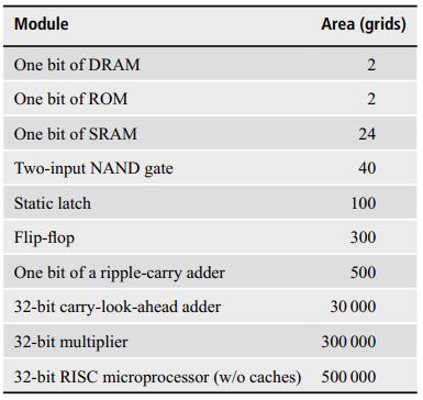
Estimate how much area you will need, using Table 2.1, to implement a module that outputs the average of the last four 32-bit input values. You will need flipflops to store the last three inputs. What about the weighted average with 32-bit arbitrary weights in ROM? How much area does it cost to
Why is the final verification stage needed at the end of Figure 2.4? Data in Figure 2.4 Simulated verification Synthesis HDL design capture Place & route Timing & power 100 analysis Final verification Formal verification Floorplanning Final design checks
If tasked with creating an air-bag deployment system for cars, what components will you need? What will you buy off the shelf and what will you design? Why? At minimum, you will need accelerometers, an actuator, and a centralized controller.
As part of your design, you have been tasked with purchasing a USB controller. Find a vendor (online) that sells USB controllers and download two different data sheets and pricings. What are the key differences?
Reduce the following Boolean expression to a minimum number of literals: (ХЛУЛz) V (ХЛУ) V (х^УЛz).
Find an image of a computer motherboard online or examine your own computer. Identify and explain the functions of at least three different chips found on the motherboard. You are not allowed to select the CPU, graphics processor, or DRAM as one of your chips.
Reduce the following Boolean expression to a minimum number of literals: (r^y) V (X^ ((wΛ2) V (wΛΞ))).
Sketch the escape pattern of 32 wires (eight on each side) from a chip to a connector at a different part of a board. Assume all wires must be routed on the surface of the board and cannot cross over each other.
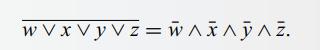
Using perfect induction, prove De Morgan’s theorem with four variables, specifically And WAX^y^2=wvxvjvz
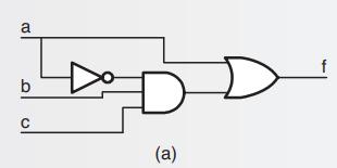
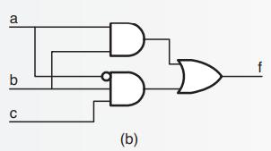
Draw a schematic for the following un simplified logic equation: f(x, y, z) = (x^y) V z.
In 2015, some manufacturers introduced 14 nm processors. If we assume that gate lengths scale with the square root of the number of transistors as given by Moore’s law, in what year will gate lengths be five silicon atoms across?
Showing 100 - 200
of 216
1
2
3
Step by Step Answers