New Semester
Started
Get
50% OFF
Study Help!
--h --m --s
Claim Now
Question Answers
Textbooks
Find textbooks, questions and answers
Oops, something went wrong!
Change your search query and then try again
S
Books
FREE
Study Help
Expert Questions
Accounting
General Management
Mathematics
Finance
Organizational Behaviour
Law
Physics
Operating System
Management Leadership
Sociology
Programming
Marketing
Database
Computer Network
Economics
Textbooks Solutions
Accounting
Managerial Accounting
Management Leadership
Cost Accounting
Statistics
Business Law
Corporate Finance
Finance
Economics
Auditing
Tutors
Online Tutors
Find a Tutor
Hire a Tutor
Become a Tutor
AI Tutor
AI Study Planner
NEW
Sell Books
Search
Search
Sign In
Register
study help
computer science
logic and computer design fundamentals
Logic And Computer Design Fundamentals 5th Edition M. Morris Mano, Charles Kime, Tom Martin - Solutions
How many times does the control unit refer to memory when it fetches and executes a three- word instruction using two indirect addressing- mode addresses if the instruction is(a) A computational type requiring two operands from two distinct memory locations with the return of the result to the
An instruction is stored at location 550 with its address field at location 551. The address field has the value 2410. A processor register R1 contains the number 2310. Evaluate the effective address if the addressing mode is(a) Direct;(b) Immediate;(c) Relative;(d) Indexed with R1 as the index
A computer with a register ile, but without PUSH and POP instructions, is to be used to implement a stack. The computer does have the following register indirect addressing modes:Show how these instructions can be used to provide the equivalent of PUSH and POP by using the instructions and register
Assume a computer with 8-bit words for the multiple- precision addition of two 32-bit unsigned numbers,(a) Write a program to execute the addition, using add and add with carry instructions.(b) Execute the program for the given operands. Each byte is expressed as a 2-digit hexadecimal number. 1F
A computer with an independent I/O system has the input and output instructionswhere ADRS is the address of an I/O register port. Give the equivalent instructions for a computer with memory- mapped I/O. IN R[DR] ADRS OUT ADRS R[SB]
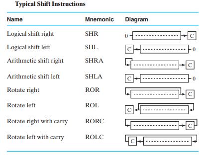
An 8-bit register contains the value 01101001, and the carry bit is equal to 1. Perform the eight shift operations given by the instructions listed in Table 9-5 as a sequence of operations on this register.Table 9-5 Typical Shift Instructions Name Logical shift right Logical shift left Arithmetic
A computer has a 32-bit word length, and all instructions are one word in length. The register ile of the computer has 16 registers.(a) For a format with no mode ields and three register addresses, what is the maximum number of opcodes possible?(b) For a format with two register address ields,
A complex instruction, push registers (PSHR), pushes the contents of all of the registers onto the stack. There are eight registers, R0 through R7, in the CPU. A corresponding instruction, POPR, pops the saved contents of the registers back from the stack into the registers.(a) Write a register
(a) Perform the logic AND, OR, and XOR with the two bytes 01101001 and 11001110.(b) Repeat part (a) with the two bytes 01010001 and 00111001.
Given the 16-bit value 1010 0101 1001 1000, what operation must be performed, and what operand is needed, in order to(a) The most significant 8 bits to 1s?(b) The bits in even positions (the leftmost bit is 15 and the rightmost bit is 0) to 0?(c) The bits in odd positions?
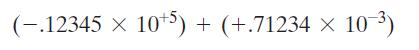
Show how the following two floating- point numbers are to be added to get a normalized result: (-.12345 10+5) + (+.71234 10-) X
A 36-bit floating- point number consists of 26 bits plus sign for the fraction and 8 bits plus sign for the exponent. What are the largest and smallest positive nonzero quantities for normalized numbers?
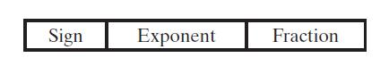
There are many possible formats for floating point numbers. Consider the following 10-formatwhere the sign ield is one bit (1: negative, 0: positive), the exponent ield is 4 bits with an excess 8 number for the bias, and the fraction ield is a 5-bit normalized number (i.e., for all numbers except
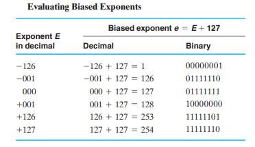
A 4-bit exponent uses an excess 7 number for the bias. List all biased binary exponents from +8 through -7.
The IEEE standard double-precision floating-point operand format consists of 64 bits. The sign occupies 1 bit, the exponent has 11 bits, and the fraction occupies 52 bits. The exponent bias is 1023 and the base is 2. There is an implied bit to the left of the binary point in the fraction. Infinity
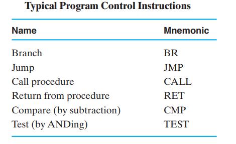
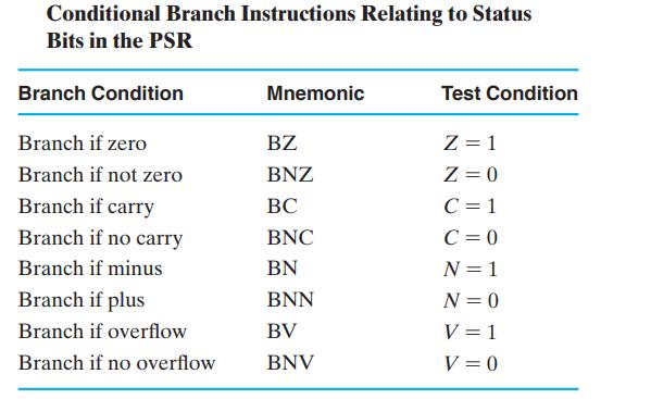
It is necessary to branch to ADRS if the bit in the least significant position of the operand in a 16-bit register is equal to 1. Show how this can be done with the TEST (Table 9-7) and BNZ (Table 9-8) instructions.Table 9-7Table 9-8 Typical Program Control Instructions Name Branch Jump Call
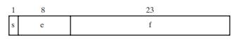
The IEEE standard single- precision floating- point format shown in Figure 9-8 uses 32 bits. Figure 9-8(a) What is the 8-digit hexadecimal representation of the decimal number -9.359375?(b) What decimal number is represented by the hexadecimal value 41CBA000? - s 8 e 23 f
Prove that if the equality 2x = 10y holds, then y = 0.3x. Using this relationship, calculate the largest and smallest normalized floating- point numbers in decimal that can be accommodated in the single- precision IEEE format.
Consider the two 8-bit numbers A = 10110110 and B = 00110111.(a) Give the decimal equivalent of each number, assuming that (1) they are unsigned and (2) they are signed 2s complement.(b) Add the two binary numbers and interpret the sum, assuming that the numbers are (1) unsigned and (2) signed 2s
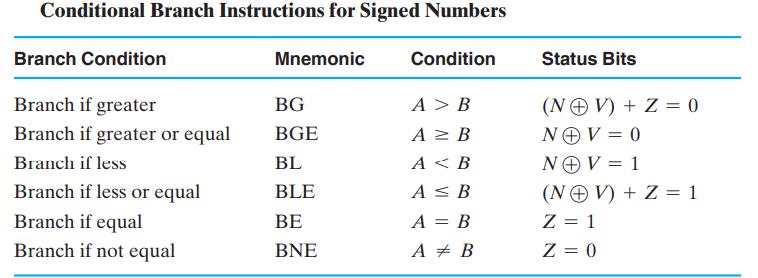
The program in a computer compares two signed 2s complement numbers A and B by performing subtraction A - B and updating the status bits. For operands let A = 11011010 and B = 01110110,(a) Evaluate the difference and interpret the binary result.(b) Determine the value of status bits N (sign), Z
Repeat Problem 9-28 with A = 10100100 and B = 10101001.Problem 9-28The program in a computer compares two signed 2s complement numbers A and B by performing subtraction A - B and updating the status bits. For operands let A = 11011010 and B = 01110110,(a) Evaluate the difference and interpret the
The program in a computer compares two unsigned numbers A and B by performing a subtraction A - B and updating the status bits. For operands let A = 01011101 and B = 01011100,(a) Evaluate the difference and interpret the binary result.(b) Determine the values of status bits C (borrow) and Z
The top of a memory stack contains 5000. The stack pointer SP contains 4000. A two- word procedure call instruction is located in memory at address 2000, followed by the address ield of 502 at location 2001. All of these are decimal values. What are the contents of PC, SP, and the top of the
What are the basic differences between a branch, a procedure call, and a program interrupt?
A computer responds to an interrupt request signal by pushing onto the stack contents of the PC and the current PSR. The computer then reads new PSR contents from memory from the location given by the interrupt vector address (IVAD). The irst address of the service program is taken from memory at
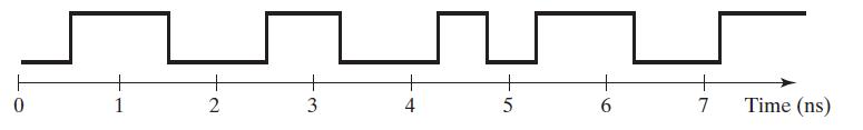
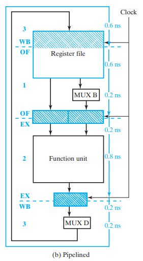
A pipelined datapath is similar to that in Figure 10-1(b), but with the delays from the top to the bottom replaced by the following values: 0.5 ns, 0.5 ns, 0.1 ns, 0.1 ns, 0.7 ns, 0.1 ns, and 0.1 ns. Determine(a) The maximum clock frequency.(b) The latency time.(c) The maximum throughput for
Assume that a computer has eight general purpose registers R0–R7, a stack pointer register SP, and program counter PC. If the calling convention for this computer is that registers R0 and R1 are used to pass parameter values to a procedure, register R2 is used to return a value to the calling
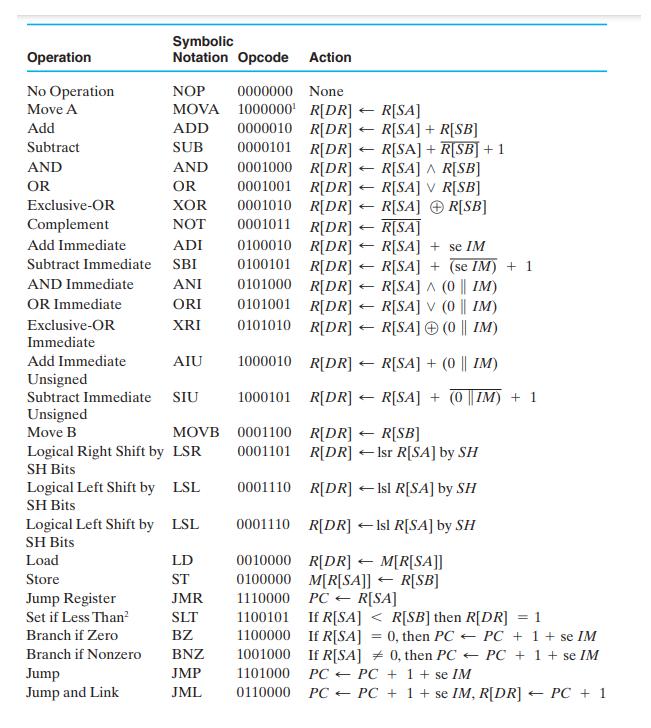
For each of the RISC operations in Table 10-1, list the addressing mode or modes used.Table 10-1 Operation No Operation Move A Add Subtract AND OR Exclusive-OR Complement Add Immediate Subtract Immediate AND Immediate OR Immediate Exclusive-OR Immediate Symbolic Notation Opcode Action NOP 0000000
A program consisting of a sequence of ten instructions without branch or jump instructions is to be executed in an 8-stage pipelined RISC computer with a clock period of 0.5 ns. Determine(a) The latency time for the pipeline(b) The maximum throughput for the pipeline.(c) The time required for
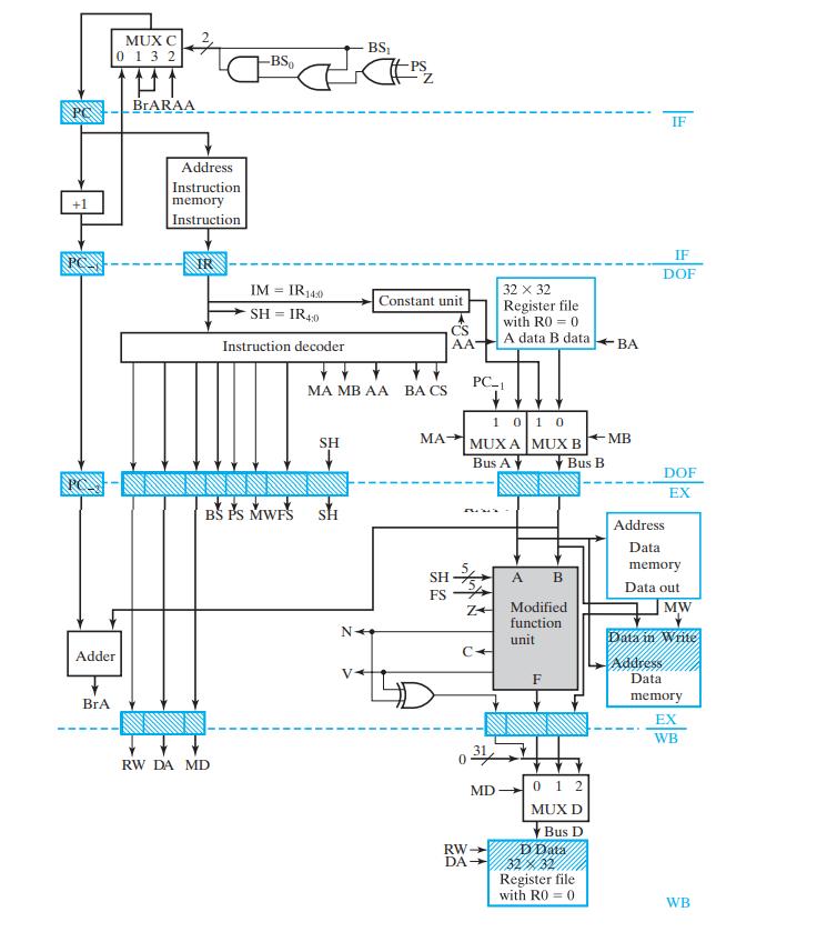
Repeat Problem 10-6 for the instruction LSR R6 R2 001D with R6 containing 00000000 and R2 containing 01ABCDEF.Problem 10-6For the RISC CPU in Figure 10-8, manually simulate, in hexadecimal, the processing of the instruction ADI R1 R16 2F01 located in PC = 10F.Assume that R16 contains 0000001F. Show
The sequence of seven LDI instructions in the register-number program with the pipeline execution pattern given on page 540 is fetched and executed. Manually simulate the execution by giving, for each clock cycle, the values in pipeline registers PC, IR, Data A, Data B, Data F, Data I, and in the
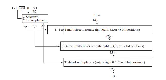
Simulate the operation of the barrel shifter in Figure 10-9 for each of the following shifts and A = 3DF3CB4A16. List the hexadecimal values on the 47 lines, 35 lines, and 32 lines out of the three levels of the shifter.(a) Right, SH = 0F(b) Left, SH = 1DFigure 10-9 Left/right 0 SH +54 Selective
For the RISC CPU in Figure 10-8, manually simulate, in hexadecimal, the processing of the instruction ADI R1 R16 2F01 located in PC = 10F.Assume that R16 contains 0000001F. Show the contents of each of the pipeline platforms and of the register file (the latter only when a change in value occurs)
Repeat Problem 10-6 for the instruction SLT R7 R3 R5 with R3 containing 0000F001 and R5 containing 0000000F.Problem 10-6For the RISC CPU in Figure 10-8, manually simulate, in hexadecimal, the processing of the instruction ADI R1 R16 2F01 located in PC = 10F.Assume that R16 contains 0000001F. Show
Repeat Problem 10-6 for the instruction SIU R2 R2 635A with R2 containing 0A5FBC2B.Problem 10-6For the RISC CPU in Figure 10-8, manually simulate, in hexadecimal, the processing of the instruction ADI R1 R16 2F01 located in PC = 10F.Assume that R16 contains 0000001F. Show the contents of each of
Use a computer-based logic minimization program to design the instruction decoder for a RISC from Table 10-3. Create an HDL model of your design and verify its correctness in simulation.Table 10-3 Control Words for Instructions Symbolic Notation Action NOP None MOVA R[DR] 1 R[SA] ADD R[DR] SUB AND
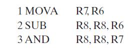
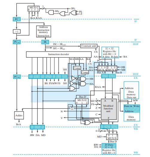
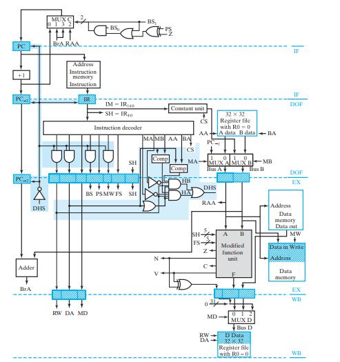
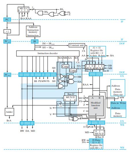
For the RISC design, draw the execution diagram for the following RISC program, and indicate any data hazards that are present: 1 MOVA 2 SUB 3 AND R7, R6 R8, R8, R6 R8, R8, R7
Draw the execution diagrams for the program in Problem 10-11, assumingProblem 10-11For the RISC design, draw the execution diagram for the following RISC program, and indicate any data hazards that are present:(a) RISC CPU with data stall given in Figure 10-12.Figure 10-12(b) RISC CPU with data
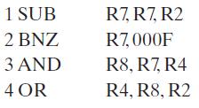
For the RISC design, draw the execution diagram for the following RISC program (with the contents of R7 nonzero after the subtraction), and indicate any data or control hazards that are present: 1 SUB 2 BNZ 3 AND 4 OR R7, R7, R2 R7, 000F R8, R7, R4 R4, R8, R2
Rewrite the RISC programs in Problems 10-11 and 10-12, using NOPs to avoid all data and control hazards, and draw the new execution diagrams.Problem 10-11For the RISC design, draw the execution diagram for the following RISC program, and indicate any data hazards that are present:Problem 10-12For
Simulate the processing of the program in Problem 10-12 using the RISC CPU with data-hazard stall in Figure 10-12. Give the contents of each pipeline platform and the register file (the latter only whenever a change occurs) for each clock cycle. Initially, R2 contains 0000001016, R4 contains
Repeat Problem 10-15 using the RISC CPU with data forwarding in Figure 10-13.Problem 10-15Simulate the processing of the program in Problem 10-12 using the RISC CPU with data-hazard stall in Figure 10-12. Give the contents of each pipeline platform and the register file (the latter only whenever a
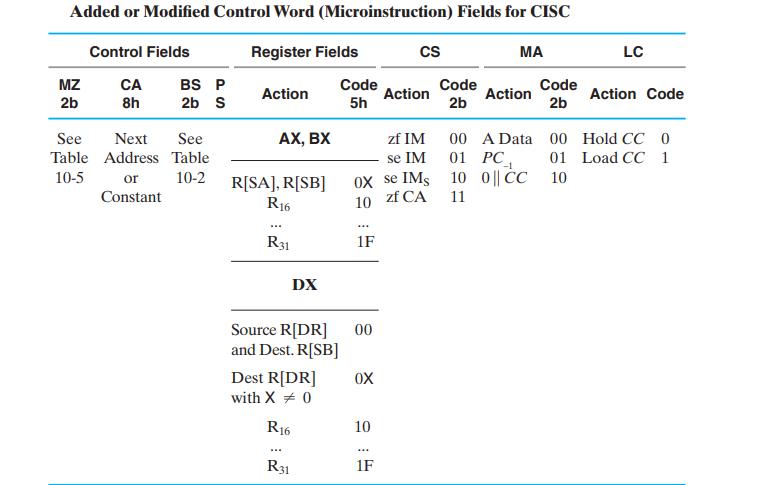
Design the constant unit in the pipelined CISC CPU by using the information given in Table 10-4 and multiple-bit multiplexers, AND gates, OR gates, and inverters. Create an HDL model of your design and verify its correctness in simulation.Table 10-4 Added or Modified Control Word (Microinstruction)
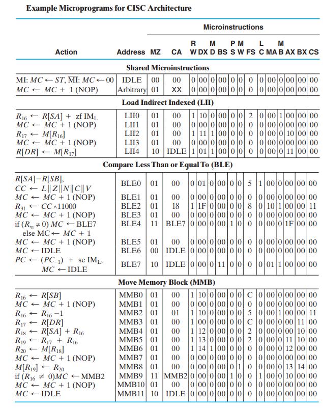
Write microcode for the execution part of each of the following CISC instructions. Give both a register transfer description and binary or hexadecimal representations similar to those shown in Table 10-6 for the binary code for each microinstruction.Table 10-6(a) Branch if overflow(b) Branch if
Repeat Problem 10-21 for the following CISC instructions that are specified by register transfer statements.Problem 10-21Write microcode for the execution part of each of the following CISC instructions. Give both a register transfer description and binary or hexadecimal representations similar to
Repeat Problem 10-22 for the following CISC instructions.Problem 10-22 Repeat Problem 10-21 for the following CISC instructions that are specified by register transfer statements.Problem 10-21Write microcode for the execution part of each of the following CISC instructions. Give both a register
Repeat Problem 10-22 for the following CISC instructions.Borrow B is defined as the complement of the carry out, C.Problem 10-22Repeat Problem 10-21 for the following CISC instructions that are specified by register transfer statements.Problem 10-21Write microcode for the execution part of each of
Repeat Problem 10-21 for the CISC instruction, Memory Scalar Add. This instruction uses the contents of R[SB] as the vector length. It adds the elements of the vector with its least significant element in memory pointed to by R[SA] and places the result in the memory location pointed to by
Repeat Problem 10-21 for the CISC instruction, Memory Vector Add. This instruction uses the contents of R[SB] as the vector length. It adds the vector with its least signiicant element in memory pointed to by R[SA] to the vector with its least signiicant element in memory pointed to by R[DR]. The
PADDB (Add Packed Byte Integers) is the mnemonic for an SSE SIMD instruction in the IA-32 architecture. In the RISC computer in this chapter, the equivalent instruction would add two 32-bit operands by adding the corresponding pairs of four bytes independently, one byte taken from each operand,
(a) In the Core 2 Duo, each core can perform a PMINSW (Minimum of Packed Signed Word Integers) instruction with two 128-bit operands, placing the result back in the irst operand. For 16-bit words, how many minimum words can be determined in parallel in the Core 2 Duo?(b) In the Cell processor,
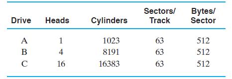
Find the formatted capacity of the hard drives described in the following table: Drive Heads A B 1 4 16 Cylinders 1023 8191 16383 Sectors/ Track 63 63 63 Bytes/ Sector 512 512 512
Estimate the time required to transfer a block of 1 MB (220 B) from a hard drive to memory given the following drive parameters: seek time, 8.5 ms; rotational delay, 4.17 ms; controller time, negligible; transfer rate, 150 MB/s.
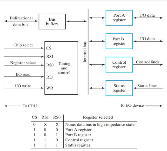
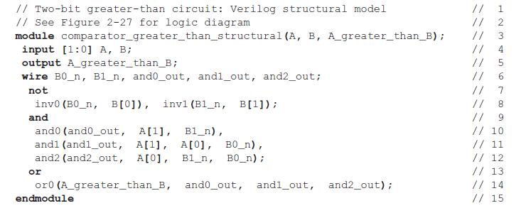
How many I/O interface units of the type shown in Figure 11-6 can be addressed by using a 16-bit address, assuming(a) Each of the chip select (CS) lines is attached to a different address line?(b) Address bits are fully decoded to form the chip select inputs?Figure 11-6 Bidirectional data bus
Find the number of pixels and subpixels for LCD screens with the following actual screen sizes:(a) 1280 х 1024.(b) 1600 х 1200.(c) 1680 х 1050.(d) 1920 х 1200.
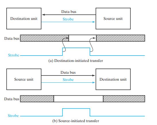
Assume that the transfers with strobing shown in Figure 11-7 are between a CPU on the left and an I/O interface on the right. There is an address coming from the CPU for each of the transfers, both of which are initiated by the CPU.(a) Draw block diagrams showing the interconnections for the
A different type of I/O interface does not have the RS1 and RS0 inputs. Up to two registers can be addressed by using a separate I/O read signal and I/O write signal for each address available. Assume that 25 percent of the registers at the interface with the CPU are read only, 25 percent of the
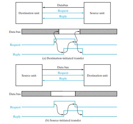
Assume that the transfers with handshaking shown in Figure 11-8 are between a CPU on the left and an I/O interface on the right. There is an address coming from the CPU for each of the transfers, both of which are initiated by the CPU.(a) Draw block diagrams, showing interconnections for the
Sketch the waveforms for the SYNC pattern used for USB and the corresponding NRZI waveform. Explain why the pattern selected is a good choice for achieving synchronization.
The following stream of data is to be transmitted by USB: 01111111001000000001101110000011(a) Assuming bit stuffing is not used, sketch the NRZI waveform.(b) Modify the stream by applying bit stuffing.(c) Sketch the NRZI waveform for the result in (b).
The 8-bit ASCII word “Bye” is to be transmitted to a device address 39 and endpoint 2. List the Output and Data 0 packets and the Handshake packet for a Stall for this transmission prior to NRZI encoding.
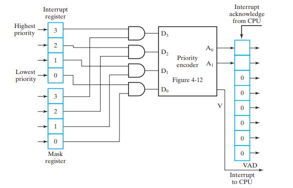
What changes are needed in Figure 11-17 to make the four VAD values equal to the binary equivalent of 024, 025, 026, and 027?Figure 11-17 Interrupt register Highest 3 priority Lowest priority 1 1 2 1 0 3 2 1 0 Mask register D3 D D Do Ao Priority encoder A Figure 4-12 Interrupt acknowledge from
Repeat Problem 11-13 for the word “Hlo” and a Handshake packet of type No Acknowledge.Problem 11-13The 8-bit ASCII word “Bye” is to be transmitted to a device address 39 and endpoint 2. List the Output and Data 0 packets and the Handshake packet for a Stall for this transmission prior to
Repeat Problem 11-18 for VAD values 122, 123, 124, and 125.Problem 11-18What changes are needed in Figure 11-17 to make the four VAD values equal to the binary equivalent of 024, 025, 026, and 027?Figure 11-17 Interrupt register Highest 3 priority Lowest priority 1 1 2 1 0 3 2 1 0 Mask register
Design parallel priority interrupt hardware for a system with six interrupt sources.
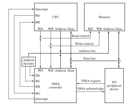
It is necessary to transfer 2048 words from a hard drive to a section of memory starting from address 4096. The transfer is by means of DMA, as shown in Figure 11-20.Figure 11-20(a) Give the initial values that the CPU must transfer to the DMA controller.(b) Give the step-by-step account of the
A priority structure is to be designed that provides vector addresses.(a) Obtain the condensed truth table of a 16 × 4 priority encoder.(b) The four outputs w, x, y, z from the priority encoder are used to provide an 8-bit vector address in the form 10wxyz01. List the 16 addresses, starting from
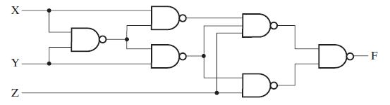
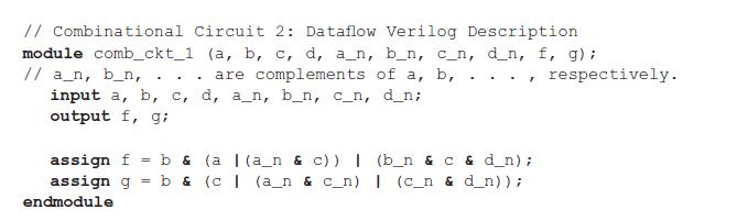
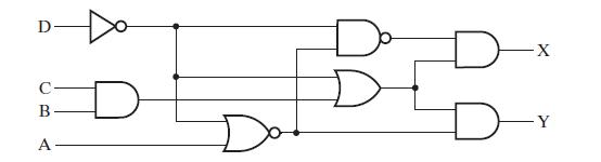
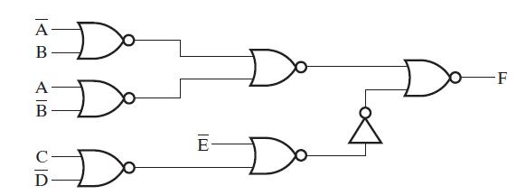
Write a datalow Verilog description for the circuit in Figure 2-43 by using the Boolean equation for the output F and using Figure 2-34 as a model.Figure 2-43Figure 2-34
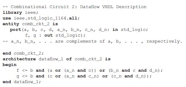
Find a logic diagram representing minimum 2-level logic needed to implement the Verilog datalow description in Figure 2-47. Note that complemented inputs are available.Figure 2-47
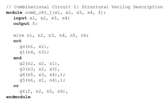
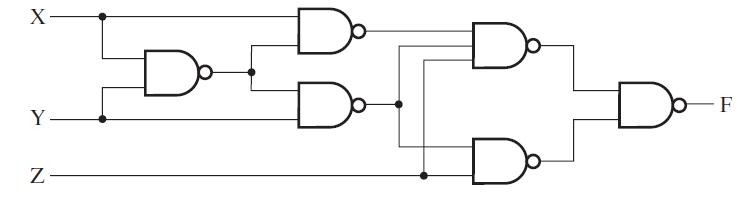
Using Figure 2-46 as a framework, write a structural Verilog description of the circuit in Figure 2-43. Replace X, Y, and Z with input [2:0] X. Compile and simulate your Verilog model for all eight possible input combinations to verify your description’s correctness.Figure 2-46Figure 2-43
Using Figure 2-33 as a framework, write a structural Verilog description of the circuit in Figure 2-44. Compile and simulate your Verilog model for all 16 possible input combinations to verify your description’s correctness.Figure 2-33Figure 2-44
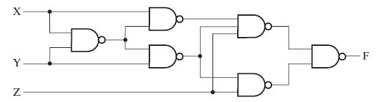
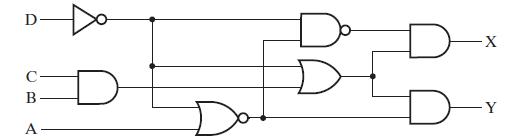
Find a logic diagram that corresponds to the Verilog structural description in Figure 2-46. Note that complemented inputs are not available.Figure 2-46
Write a datalow VHDL description for the circuit in Figure 2-43 by using the Boolean equation for the output F. Figure 2-43
Find a logic diagram representing minimum two- level logic needed to implement the VHDL datalow description in Figure 2-45. Note that complemented inputs are available.Figure 2-45
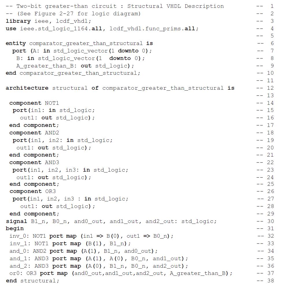
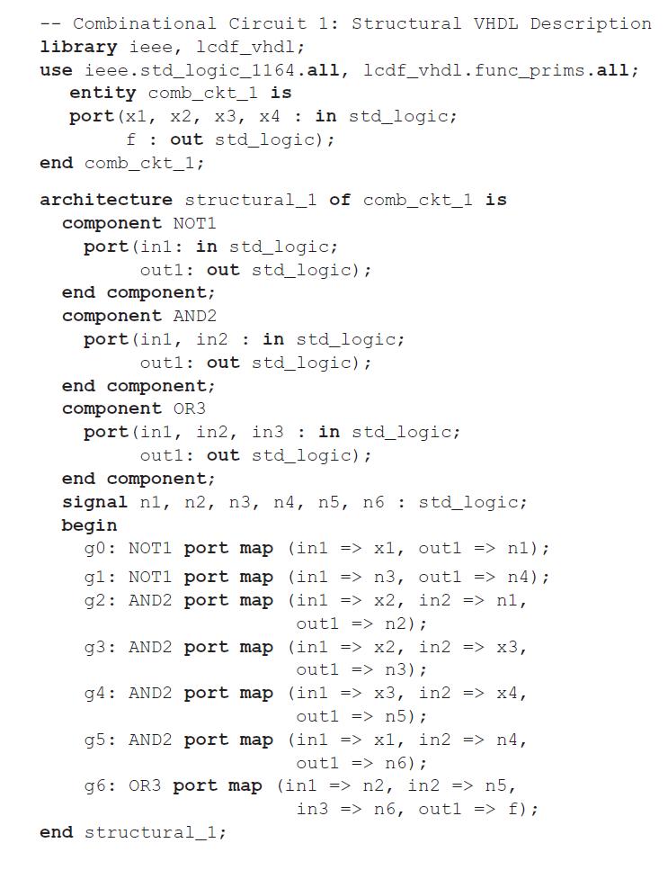
Using Figure 2-28 as a framework, write a structural VHDL description of the circuit in Figure 2-44. Consult package func_prims in library lcdf_vhdl for information on the various gate components. Compile func_prims and your VHDL model, and simulate your VHDL model for all 16 possible input
Using Figure 2-28 as a framework, write a structural VHDL description of the circuit in Figure 2-43. Replace X, Y, and Z with X (2:0). Consult package func_prims in library lcdf_vhdl for information on the various gate components. Compile func_prims and your VHDL model, and simulate your VHDL model
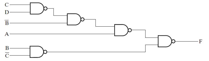
*Find a logic diagram that corresponds to the VHDL structural description in Figure 2-42. Note that complemented inputs are not available.Figure 2-42
For a given gate, tPHL = 0.05 ns and tPLH = 0.10 ns. Suppose that an inertial delay model is to be developed from this information for typical gate-delay behavior.(a) Assuming a positive output pulse (LHL), what would the propagation delay and rejection time be?(b) Discuss the applicability of
The rejection time for inertial delays is required to be less than or equal to the propagation delay. In terms of the discussion of the example in Figure 2-25, why is this condition necessary to determine the delayed output?Figure 2-25
Assume that tpd is the average of tPHL and tPLH. Find the delay from each input to the output in Figure 2-41 by(a) Finding tPHL and tPLH for each path, assuming tPHL = 0.20 ns and tPLH = 0.36 ns for each gate. From these values, ind tpd for each path.(b) Using tpd = 0.28 ns for each
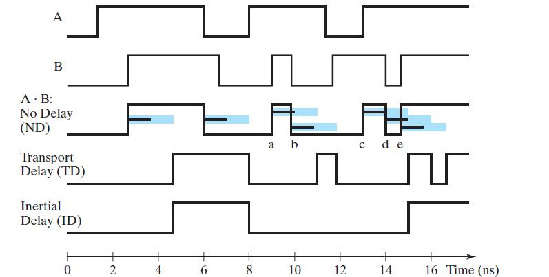
The waveform in Figure 2-40 is applied to an inverter. Find the output of the inverter, assuming that(a) It has no delay.(b) It has a transport delay of 0.06 ns.(c) It has an inertial delay of 0.06 ns with a rejection time of 0.04 ns. Figure 2-40
The NOR gates in Figure 2-39 have propagation delay tpd = 0.073 ns and the inverter has a propagation delay tpd = 0.048 ns. What is the propagation delay of the longest path through the circuit? Figure 2-39
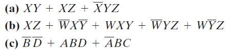
Implement the following Boolean function with exclusive- OR and AND gates, using a minimum number of gate inputs:
Prove that the dual of the exclusive-OR is also its complement.
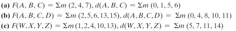
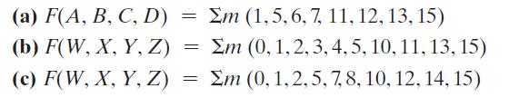
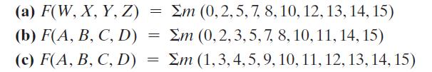
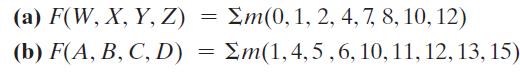
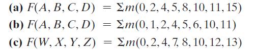
Optimize the following Boolean functions F together with the don’t-care conditions d in (1) sum-of-products and (2) product-of-sums form:
Optimize the following Boolean functions F together with the don’t-care conditions d. Find all prime implicants and essential prime implicants, and apply the selection rule.
Optimize the following Boolean functions F together with the don’ t-care conditions d:
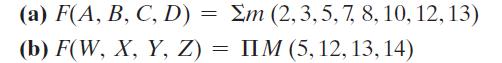
Optimize the following functions into (1) sum-of-products and (2) product-of-sums forms:
Optimize the following expressions in (1) sum-of-products and (2) product-of-sums forms:
Optimize the following Boolean functions in product- of- sums form:
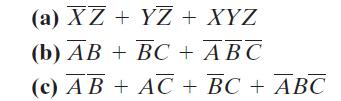
Optimize the following Boolean functions by inding all prime implicants and essential prime implicants and applying the selection rule:
Find all the prime implicants for the following Boolean functions, and determine which are essential:
Find the minterms of the following expressions by irst plotting each expression on a map:
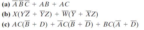
Optimize the following Boolean functions, using a map:
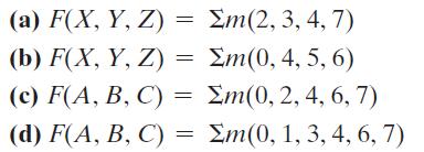
Optimize the following Boolean functions by means of a 4-variable map:
Optimize the following Boolean expressions using a map:
Optimize the following Boolean functions by means of a 3-variable map:
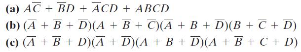
Draw the logic diagram for the following Boolean expressions. The diagram should correspond exactly to the equation. Assume that the complements of the inputs are not available.
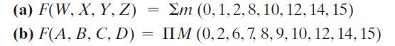
Convert the following expressions into sum- of- products and product-of-sums forms:
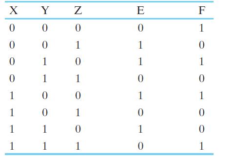
For the Boolean functions E and F, as given in the following truth table:
Showing 300 - 400
of 439
1
2
3
4
5
Step by Step Answers
![Register indirect + increment: LD Rj Ri ST Rj Ri Decrement + register indirect: LD Rj Ri ST Rj Ri Rj+M[Ri]](https://dsd5zvtm8ll6.cloudfront.net/images/question_images/1704/5/7/0/9336599b0353eae91704570929561.jpg)
![IN R[DR] ADRS OUT ADRS R[SB]](https://dsd5zvtm8ll6.cloudfront.net/images/question_images/1704/5/7/0/9696599b0592cda91704570967383.jpg)
![Control Words for Instructions Symbolic Notation Action NOP None MOVA R[DR] 1 R[SA] ADD R[DR] SUB AND OR XOR](https://dsd5zvtm8ll6.cloudfront.net/images/question_images/1704/5/7/3/5126599ba48092f31704573508297.jpg)

![(a) Push: R[SA] DR=SA. R[SA] + 1 followed by M[R[SA]] R[SB]. Assume (b) Pop: R[DR] M[R[SA]] followed by](https://dsd5zvtm8ll6.cloudfront.net/images/question_images/1704/5/7/4/5426599be4e5df141704574540551.jpg)
![(a) Add Memory Indirect: R[DR] (b) Add to Memory: M[R[DR]] M[R[SA]] + R[SB] R[SA] + M[M[R[SB]]]](https://dsd5zvtm8ll6.cloudfront.net/images/question_images/1704/5/7/4/6346599beaac3b041704574632958.jpg)
![(a) Add with carry: R[DR] R[SA] + R[SB] + C (b) Subtract with borrow: R[DR] R[SA] R[SB] - B -](https://dsd5zvtm8ll6.cloudfront.net/images/question_images/1704/5/7/4/6116599be93340691704574609329.jpg)