New Semester
Started
Get
50% OFF
Study Help!
--h --m --s
Claim Now
Question Answers
Textbooks
Find textbooks, questions and answers
Oops, something went wrong!
Change your search query and then try again
S
Books
FREE
Study Help
Expert Questions
Accounting
General Management
Mathematics
Finance
Organizational Behaviour
Law
Physics
Operating System
Management Leadership
Sociology
Programming
Marketing
Database
Computer Network
Economics
Textbooks Solutions
Accounting
Managerial Accounting
Management Leadership
Cost Accounting
Statistics
Business Law
Corporate Finance
Finance
Economics
Auditing
Tutors
Online Tutors
Find a Tutor
Hire a Tutor
Become a Tutor
AI Tutor
AI Study Planner
NEW
Sell Books
Search
Search
Sign In
Register
study help
computer science
logic and computer design fundamentals
Logic And Computer Design Fundamentals 5th Edition M. Morris Mano, Charles Kime, Tom Martin - Solutions
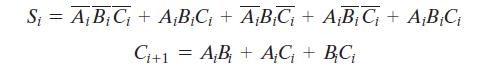
Implement the Boolean functionwith a 4–to–1-line multiplexer and external gates. Connect inputs A and B to the selection lines. The input requirements for the four data lines will be a function of the variables C and D. The values of these variables are obtained by expressing F as a function of
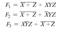
A combinational circuit is deined by the following three Boolean functions:Design the circuit with a decoder and external OR gates. F = X+Z+ XYZ F = X + Z + XYZ F3 = XYZ + X+Z
Solve Problem 3-47 using two 3–to–8-line decoders with enables, an inverter, and OR gates with a maximum fan-in of 4.Problem 3-47Implement the Boolean functionwith a 4–to–1-line multiplexer and external gates. Connect inputs A and B to the selection lines. The input requirements for the
Implement the following Boolean function with an 8–to–1-line multiplexer and a single inverter with variable D as its input: F(A, B, C, D) = m(2, 4, 6, 9, 10, 11, 15)
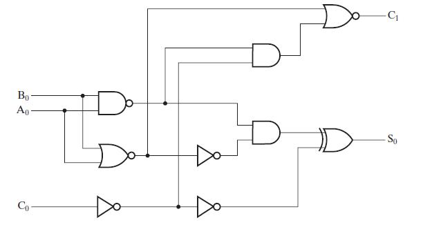
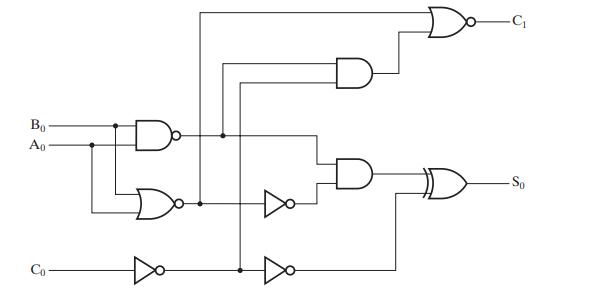
The logic diagram of the first stage of a 4-bit adder, as implemented in integrated circuit type 74283, is shown in Figure 3-58. Verify that the circuit implements a full adder.Figure 3-58 Bo Ao TD -C So
Design a combinational circuit that forms the 2-bit binary sum S1S0 of two 2-bit numbers A1A0 and B1B0 and has both a carry input C0 and carry output C2. Design the entire circuit implementing each of the three outputs with a two-level circuit plus inverters for the input variables. Begin the
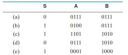
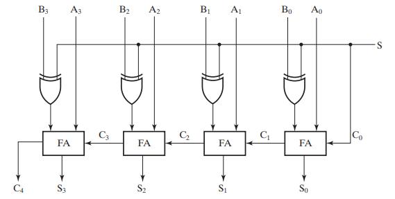
The adder–subtractor circuit of Figure 3-45 has the following values for input select S and data inputs A and B:Figure 3-45 Determine, in each case, the values of the outputs S3, S2, S1, S0, and C4. (a) (b) (c) (d) (e) S 0 1 1 0 1 A 0111 0100 1101 0111 0001 B 0111 0111 1010 1010 1000
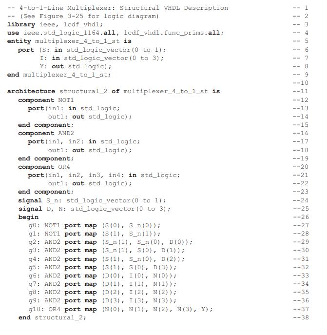
Using Figure 3-28 as a guide, write a structural VHDL description for the full-adder circuit in Figure 3-58. Compile and simulate your description. Apply all eight input combinations to check the correction function of your description.Figure 3-28Figure 3-58 4-to-1-Line Multiplexer: Structural VHDL
Perform the indicated subtraction with the following unsigned binary numbers by taking the 2s complement of the subtrahend:(a) 11010 - 10001(b) 11110 - 1110(c) 1111110 - 1111110(d) 101001 - 101
Repeat Problem 3-52, assuming the numbers are 2s complement signed numbers. Use extension to equalize the length of the operands. Indicate whether overflow occurs during the complement operations for any of the given subtrahends. Indicate whether overflow occurs overall for any of the given
Perform the arithmetic operations (+36) + (-24) and (-35) - (-24) in binary using signed 2s complement representation for negative numbers.
The following binary numbers have a sign in the leftmost position and, if negative, are in 2s complement form. Perform the indicated arithmetic operations and verify the answers.(a) 100111 + 111001(b) 001011 + 100110(c) 110001 - 010010(d) 101110 - 110111Indicate whether overflow occurs for each
Design two versions of the combinational circuit whose input is a 4-bit number and whose output is the 2s complement of the input number, for each of the following cases using AND, OR, and NOT gates:(a) The circuit is a simpliied two-level circuit, plus inverters as needed for the input
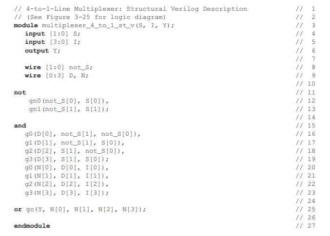
Using Figure 3-31 as a guide, write a structural Verilog description for the fulladder circuit in Figure 3-58. Compile and simulate your description. Apply all eight input combinations to check the correction function of your description.Figure 3-31Figure 3-58 // 4-to-1-Line Multiplexer: Structural
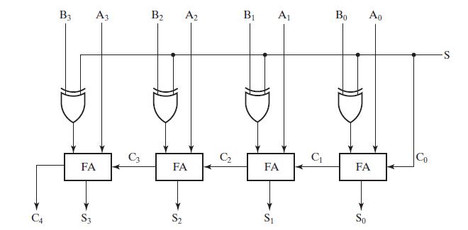
Compile and simulate the 4-bit adder in Figures 3-47 and 3-48. Apply combinations that check out the rightmost full adder for all eight input combinations; this also serves as a check for the other full adders. Also, apply combinations that check the carry chain connections between all full adders
Use contraction beginning with a 4-bit adder with carry out to design a 4-bit increment-by-2 circuit with carry out that adds the binary value 0010 to its 4-bit input. The function to be implemented is S = A + 0010.
Use contraction beginning with an 8-bit adder–subtractor without carry out to design an 8-bit circuit without carry out that increments its input by 000000101 for input S = 0 and decrements its input by 00000101 for input S = 1. Perform the design by designing the distinct 1-bit cells needed and
Design a combinational circuit that compares two 4-bit unsigned numbers A and B to see whether B is greater than A. The circuit has one output X, so that X = 1 if A < B and X = 0 if A ≥ B.
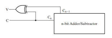
Using Figure 3-49 as a guide and a “when-else” on S from Figure 3-29, write a high-level behavior VHDL description for the adder–subtractor in Figure 3-46 (see Figure 3-45 for details). Compile and simulate your description.Assuming a ripple carry implementation, apply combinations that check
Repeat Problem 3-59 by using three-input, one-output circuits, one for each of the four bits. The four circuits are connected together in cascade by carrylike signals. One of the inputs to each cell is a carry input, and the single output is a carry output.Problem 3-59Design a combinational circuit
Compile and simulate the behavioral description of the 4-bit adder in Figure 3-49. Assuming a ripple carry implementation, apply combinations that check out the rightmost full adder for all eight input combinations. Also apply combinations that check the carry chain connections between all full
Repeat Problem 3-59 by applying contraction to a 4-bit subtractor and using the borrow out as X.Problem 3-59Design a combinational circuit that compares two 4-bit unsigned numbers A and B to see whether B is greater than A. The circuit has one output X, so that X = 1 if A < B and X = 0 if A ≥ B.
Design a combinational circuit that compares 4-bit unsigned numbers A and B to see whether A = B or A > B. Use an iterative circuit as in Problem 3-60.Problem 3-60Repeat Problem 3-59 by using three-input, one-output circuits, one for each of the four bits. The four circuits are connected together
Design a 5-bit signed-magnitude adder–subtractor. Divide the circuit for design into (1) sign generation and add–subtract control logic, (2) an unsigned number adder–subtractor using 2s complement of the minuend for subtraction, and (3) selective 2s complement result correction logic.
Using Figure 3-51 as a guide and a “binary decision” on S from Figure 3-34, write a high-level behavior Verilog description for the adder–subtractor in Figure 3-46 (see Figure 3-45 for details). Compile and simulate your description. Assuming a ripple carry implementation, apply input
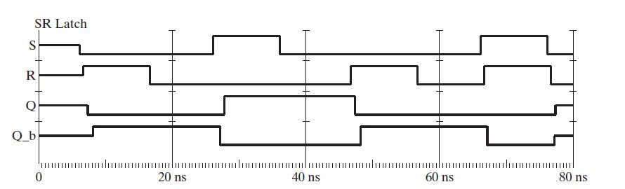
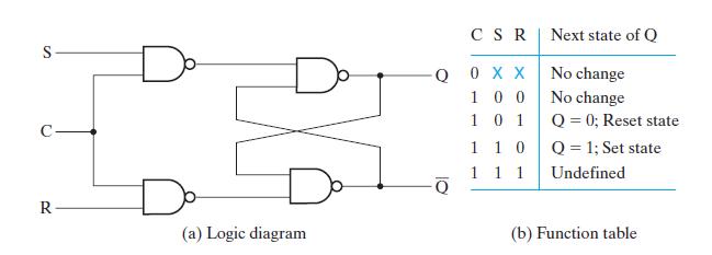
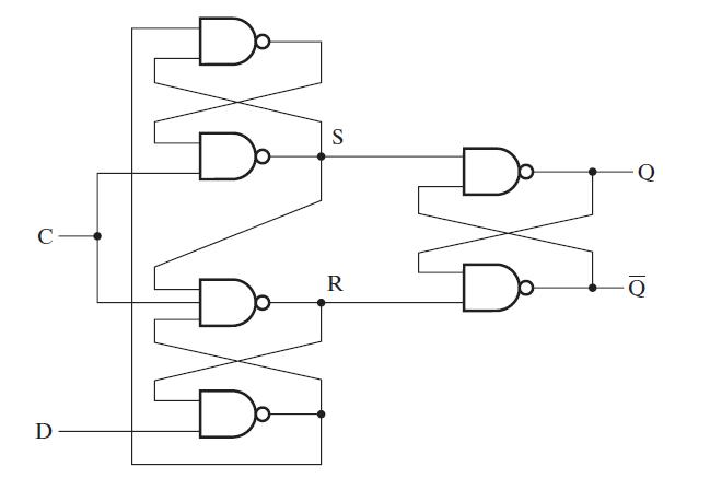
Perform a manual or computer- based logic simulation similar to that given in Figure 4-5 for the SR latch with control input C in Figure 4-7. In particular, examine the behavior of the circuit when S and R are changed while C has the value 1.Figure 4-5Figure 4-7 SR Latch S R Q_b
Compile and simulate the 4-bit adder in Figure 3-50. Apply combinations that check out the rightmost full adder for all eight input combinations; this also serves as a check for the other full adders. Also, apply combinations that check the carry chain connections between all full adders by
Compile and simulate the behavioral description of the 4-bit adder in Figure 3-51. Assuming a ripple carry implementation, apply all eight input combinations to check out the rightmost full adder. Also, apply combinations to check the carry chain connections between all full adders by demonstrating
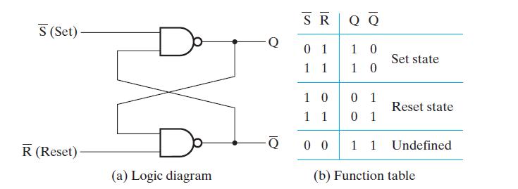
Perform a manual or computer- based logic simulation similar to that given in Figure 4-5 for the S̅R̅ latch shown in Figure 4-6. Construct the input sequence, keeping in mind that changes in state for this type of latch occur in response to 0 rather than 1.Figure 4-5Figure 4-6 SR Latch S R Q_b
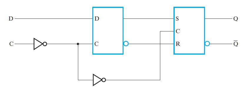
A popular alternative design for a positive- edge- triggered D lip- lop is shown in Figure 4-47. Manually or automatically simulate the circuit to determine whether its functional behavior is identical to that of the circuit in Figure 4-10.Figure 4-10Figure 4-47 D- C- D C S C R -Q
A sequential circuit with two D lip- lops A and B, one input Y, and one output Z is specified by the following input equations:(a) Draw the logic diagram of the circuit.(b) Derive the state table.(c) Derive the state diagram.(d) Is this a Mealy or a Moore machine? DA BY+AY, DB = Y, Z = AB
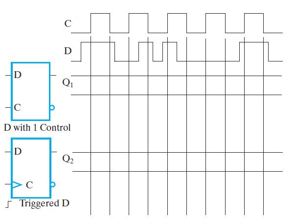
Clock and D waveforms, a D latch and an edge- triggered D lip- lop are shown in Figure 4-48. For both the latch and the lip- lop, carefully sketch the output waveform, Qi, obtained in response to the input waveforms. Assume that the propagation delay of the storage elements is negligible.
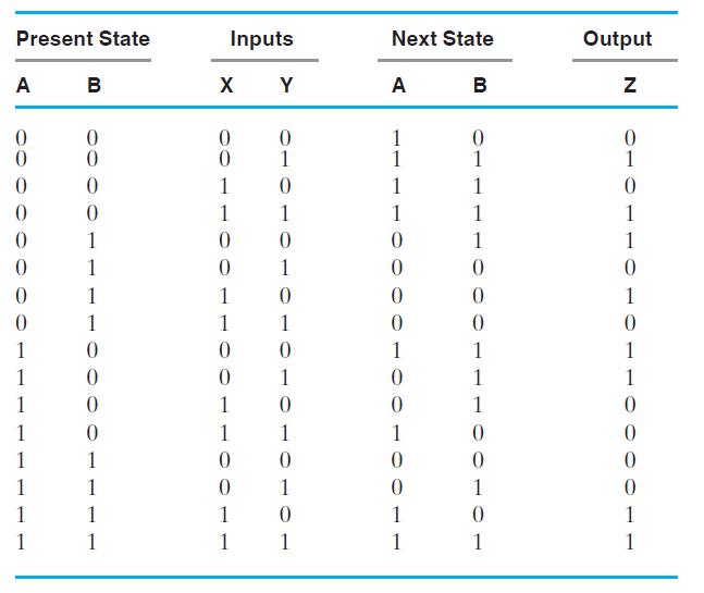
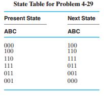
Draw the state diagram of the sequential circuit specified by the state table in Table 4-14. Present State A 0 0 0 0 0 0 0 0 1 1 1 1 1 1 1 B 0 0 0 0 1 1 1 0 0 0 0 1 1 1 Inputs X 0 0 1 1 0 0 1 1 0 0 1 1 0 0 1 1 Y 0 1 0 1 0 1 0 1 0 1 0 1 0 1 0 1 Next State A B 1 1 1 1 0 0 0 0 1 0 0 1 0 0 1 1 0 1 1 1
A sequential circuit has one lip-lop Q, two inputs X and Y, and one output S. The circuit consists of a D lip-lop with S as its output and logic implementing the functionwith D as the input to the D lip- lop. Derive the state table and state diagram of the sequential circuit. D = XOYS
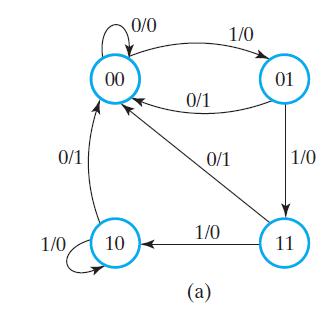
Starting from state 00 in the state diagram of Figure 4-15(a), determine the state transitions and output sequence that will be generated when an input sequence of 10011011110 is applied.Figure 4-15 (a) 0/1 1/0 00 10 0/0 0/1 0/1 1/0 1/0 (a) 01 1/0 11
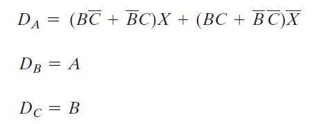
A sequential circuit has three D lip- lops A, B, and C, and one input X. The circuit is described by the following input equations:(a) Derive the state table for the circuit.(b) Draw two state diagrams, one for X = 0 and the other for X = 1. DA = (BC + (BC DB = A Dc = B + BC)X + (BC + BC)X
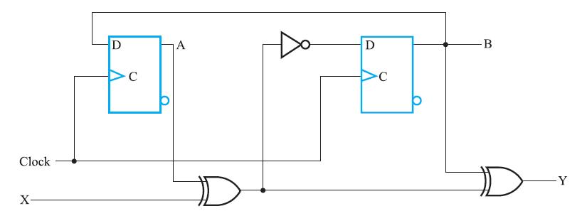
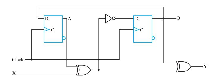
A sequential circuit has two D lip- lops, one input X, and one output Y. The logic diagram of the circuit is shown in Figure 4-49. Derive the state table and state diagram of the circuit.Figure 4-49 Clock X- D C A D C B -Y
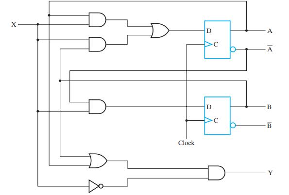
A sequential circuit is given in Figure 4-13.Figure 4-13(a) Add the necessary logic and/or connections to the circuit to provide an asynchronous reset to state A = 1, B = 0 for signal Reset = 0.(b) Add the necessary logic and/or connections to the circuit to provide a synchronous reset to state A
Design a sequential circuit with two D lip- lops A and B and one input X. When X = 0, the state of the circuit remains the same. When X = 1, the circuit goes through the state transitions from 00 to 10 to 11 to 01, back to 00, and then repeats.
The state diagram for a sequential circuit appears in Figure 4-50.Figure 4-50(a) Find the state table for the circuit.(b) Make a state assignment for the circuit using 2-bit codes and find the encoded state table.(c) Find an optimized circuit implementation using D lip- lops, NAND gates, and
The state diagram for a sequential circuit appears in Figure 4-51.Figure 4-51(a) Find the state table for the circuit.(b) Make a state assignment for the circuit using 3-bit codes for the six states;make one of the code bits equal to the output to save logic, and ind the encoded state table. The
The circuit given in Figure 4-52 is to be redesigned to cut its cost.(a) Find the state table for the circuit and replace the state codes with single- letter identiiers. States 100 and 111 were unused in the original design.(b) Check for and combine equivalent states.(c) Make a state assignment
A serial odd parity generator is to be designed. A binary sequence of arbitrary length is presented to the parity generator on input X. When a given bit is presented on input X, the corresponding odd parity bit for the binary sequence is to appear during the same clock cycle on output Z. To
A Universal Serial Bus (USB) communication link requires a circuit that produces the sequence 00000001. You are to design a synchronous sequential circuit that starts producing this sequence for input E = 1. Once the sequence starts, it completes. If E = 1, during the last output in the sequence,
Repeat Problem 4-20 for the sequence 01111110 that is used in a different communication network protocol.Problem 4-20:A Universal Serial Bus (USB) communication link requires a circuit that produces the sequence 00000001. You are to design a synchronous sequential circuit that starts producing this
Repeat Problem 4-23, designing a sequential circuit that transforms an NRZI message into a normal message. The mapping for such a circuit is as follows:(a) If a change from 0 to 1 or from 1 to 0 occurs between adjacent bits in the NRZI message, then the message bit is a 0.(b) If no change occurs
A sequential circuit has two lip- lops A and B, one input X, and one output Y. The state diagram is shown in Figure 4-54. Design the circuit with D lip- lops using a one- hot state assignment. Figure 4-54: 00/1 1 11/0 0 0 01/0 1 10/0
A computer has no stack, but instead uses register R7 as a link register (i.e., the computer stores the return address in R7).(a) Show the register transfers for a branch and link instruction.(b) Assuming that another branch and link is present in the procedure being called, what action must be
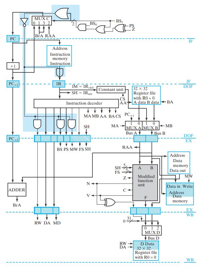
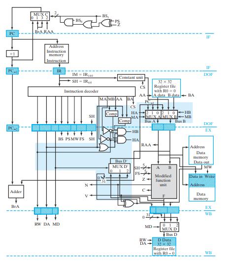
Draw the execution diagram for the program in Problem 10-12, assuming the combination of the RISC CPU with branch prediction in Figure 10-17 and the RISC CPU with data forwarding in Figure 10-13.Figure 10-17 Problem 10-12For the RISC design, draw the execution diagram for the following RISC
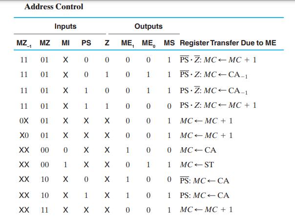
Design the address control logic described by Table 10-5 by using AND gates, OR gates, and inverters.Table 10-5 Address Control MZ Inputs MZ MI 11 01 X 11 01 X 11 01 X 11 01 X OX 01 X XO 01 X X XX 00 0 XX 00 1 X XX 10 X 0 xx PS Z 0 1 1 X xx X XX 10 X 1 XX 11 X X 0 1 0 1 X X X X X X X Outputs ME,
Explain how a DDRAM achieves a data rate that is a factor of two higher than a comparable SDRAM.
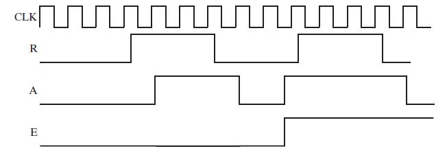
A pair of signals Request (R) and Acknowledge (A) is used to coordinate transactions between a CPU and its I/O system. The interaction of these signals is often referred to as a “handshake.” These signals are synchronous with the clock and, for a transaction, are to have their transitions
A serial leading- 1s detector is to be designed. A binary integer of arbitrary length is presented to the serial leading- 1s detector, most significant bit first, on input X. When a given bit is presented on input X, the corresponding output bit is to appear during the same clock cycle on output Z.
The state table for a 3-bit twisted ring counter is given in Table 4-15. This circuit has no inputs, and its outputs are the uncomplemented outputs of the lip- lops. Since it has no inputs, it simply goes from state to state whenever a clock pulse occurs. It has an asynchronous reset that
Do an automatic logic simulation- based verification of your design in Problem 4-14. The input sequence used in the simulation should include all transitions in Figure 4-50. The simulation output should include the input X and the state variables A, B, and output Z.Problem 4-14:The state diagram
Generate a verification sequence for the circuit described by the state table in Table 4-14. To reduce the length of the simulation sequence, assume that the simulator can handle X inputs and use X’s whenever possible. Assume that a Reset input is available to initialize the state to A = 0, B = 0
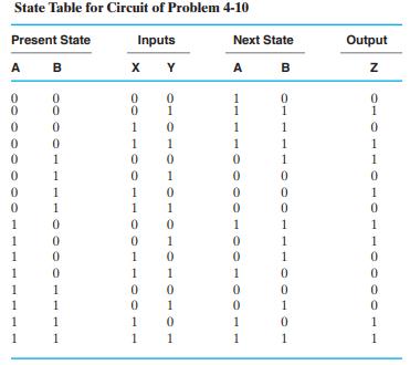
Design the circuit specified by Table 4-14 and use the sequence from Problem 4-31 (either yours or the one posted on the text website) to perform an automatic logic simulation- based verification of your design.Table 4-14: State Table for Circuit of Problem 4-10 Present State Inputs Y A B 00000 0 0
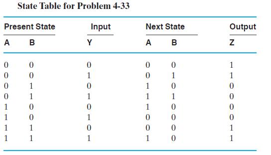
The state table for a sequential circuit is given in Table 4-16.(a) Draw the state diagram for the circuit.(b) Implement the circuit using D lip- lops and minimal input functions for each lip- lop. Reset is asynchronous and active low (RESET = 0), and initializes the state to A = 0, B = 0.Table
Find a state-machine diagram that is equivalent to the state diagram in Figure 4-55. Reduce the complexity of the transition conditions as much as possible. Attempt to make outputs unconditional by changing Mealy outputs to Moore outputs. Make a state assignment to your state- machine diagram and
Design the sequential circuit for the state- machine diagram from Problem 4-35. Use a one- hot state assignment, D lip- lops and AND gates, OR gates, and inverters.Problem 4-35:Find a state-machine diagram that is equivalent to the state diagram in Figure 4-55. Reduce the complexity of the
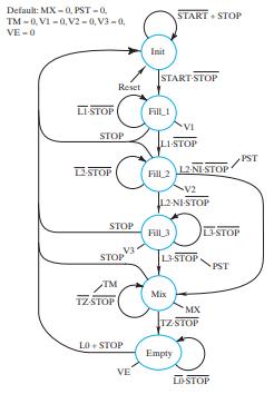
(a) Verify that the transitions in the state- machine diagram in Figure 4-27 obey the two transition conditions for state diagrams.(b) Repeat part(a) for the state-machine diagram in Figure 4-28.Figure 4-27:Figure 4-28: Default: MX-0, PST-0, TM-0, V1-0. V2-0, V3-0, VE-0 LI-STOP STOP L2-STOP FO
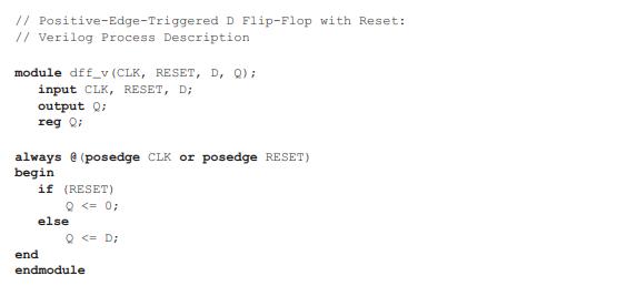
Design a new type of positive-edge-triggered lip-lop called the LH lip-lop. It has a clock C, a data input D, and a load input L. If, at the positive edge of C, L equals 1, then the data on D is stored in the lip-lop. If, at the positive edge of C, L equals 0, then the current stored value in the
You are to find the state- machine diagram for the following electronic vending-machine specification. The vending machine sells jawbreaker candy, one jawbreaker for 25¢. The machine accepts N (nickels = 5¢), D (dimes = 10¢), and Q (quarters = 25¢). When the sum of the coins inserted in
Write a gate- level structural VHDL description for the circuit from Problem 4-11. Use the VHDL model for a D lip- lop from Figure 4-29. Use the package func_prims in library lcdf_vhdl for the logic gate components.Problem 4-11:A sequential circuit has two D lip- lops, one input X, and one output
You are to find the state- machine diagram for the following electronic vending- machine specification. The vending machine sells soda for $1.50 per bottle. The machine accepts only D ($1 bills) and Q (quarters = 25¢). When the sum of money is greater than $1.50, i.e., two $1 bills, the machine
Write a behavioral VHDL description for the circuit from Problem 4-11 using a process to describe the state diagram.Problem 4-11:A sequential circuit has two D lip- lops, one input X, and one output Y. The logic diagram of the circuit is shown in Figure 4-49. Derive the state table and state
Although this chapter has introduced VHDL processes to describe sequential circuits, combinational circuits can also be described using processes. Write a VHDL description for the multiplexer in Figure 3-25 by using a process containing a case statement rather than the continuous assignment
Repeat Problem 4-42 by using a VHDL process containing if- then- else statements.Problem 4-42:Although this chapter has introduced VHDL processes to describe sequential circuits, combinational circuits can also be described using processes. Write a VHDL description for the multiplexer in Figure
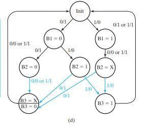
Write a VHDL description for the sequential circuit with the state diagram given by Figure 4-19(d). Include an asynchronous RESET signal to initialize the circuit to state Init. Compile your description, apply an input sequence to pass through every transition of the state diagram at least once,
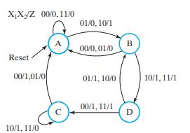
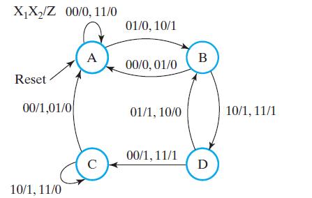
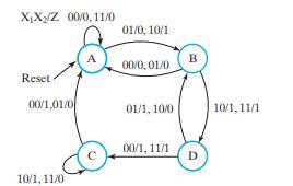
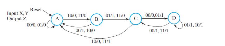
Write a VHDL description for the circuit specified in Problem 4-14.Problem 4-14:The state diagram for a sequential circuit appears in Figure 4-50.Figure 4-50: XX/Z 00/0, 11/0 Reset 00/1,01/0 10/1, 11/0 A 01/0, 10/1 00/0,01/0 01/1, 10/0 00/1, 11/1 B D 10/1, 11/1
Write a VHDL description for the state- machine diagram for the batch mixing system derived in Example 4-10.Example 4-10:A mixing system for large batches of liquids is designed to add up to three ingredients to a large circular mixing tank, mix the ingredients, and then empty the mixed liquid from
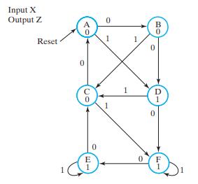
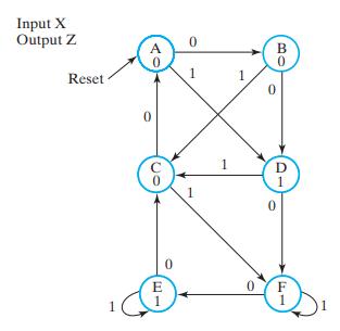
Write a VHDL description for the circuit specified in Problem 4-15.Problem 4-15:The state diagram for a sequential circuit appears in Figure 4-51.Figure 4-51: Input X Output Z Reset 1 A 0 0 0 0 E 1 0 1 1 1 0 30 B 0 D 1 0 F
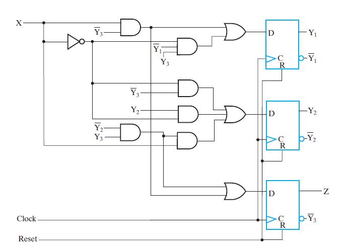
Write a gate- level structural Verilog description for the circuit from Problem 4-11. Use the Verilog model for a D lip- lop from Figure 4-33.Problem 4-11:A sequential circuit has two D lip- lops, one input X, and one output Y. The logic diagram of the circuit is shown in Figure 4-49. Derive the
Write a VHDL description for the state- machine diagram for the jawbreaker vending machine described in Problem 4-38. You may obtain the state- machine diagram by either solving Problem 4-38 or finding its solution on the textbook website.Problem 4-38:You are to ind the state- machine diagram for
Write a behavioral Verilog description for the circuit from Problem 4-11 using a process to describe the state diagram.Problem 4-11:A sequential circuit has two D lip- lops, one input X, and one output Y. The logic diagram of the circuit is shown in Figure 4-49. Derive the state table and state
Repeat Problem 4-51 by using a Verilog process containing if- else statements.Problem 4-51:Although this chapter has introduced Verilog processes to describe sequential circuits, combinational circuits can also be described using processes. Write a Verilog description for the multiplexer in Figure
Although this chapter has introduced Verilog processes to describe sequential circuits, combinational circuits can also be described using processes. Write a Verilog description for the multiplexer in Figure 3-25 by using a process containing a case statement rather than the continuous assignment
Write a Verilog description for the sequential circuit given by the state diagram in Figure 4-19(d). Include an asynchronous RESET signal to initialize the circuit to state Init. Compile your description, apply an input sequence to pass through every arc of the state diagram at least once, and
Write a Verilog description for the circuit speciied in Problem 4-14.Problem 4-14The state diagram for a sequential circuit appears in Figure 4-50.Figure 4-50: XX/Z 00/0, 11/0 Reset 00/1,01/0 10/1, 11/0 A 01/0, 10/1 00/0,01/0 01/1, 10/0 00/1, 11/1 B D 10/1, 11/1
Write a Verilog description for the state-machine diagram for the batch mixing system derived in Example 4-10.Example 4-10:A mixing system for large batches of liquids is designed to add up to three ingredients to a large circular mixing tank, mix the ingredients, and then empty the mixed liquid
Write a Verilog description for the circuit speciied in Problem 4-15.Problem 4-14:The state diagram for a sequential circuit appears in Figure 4-50.Figure 4-50: XX/Z 00/0, 11/0 Reset 00/1,01/0 10/1, 11/0 A 01/0, 10/1 00/0,01/0 01/1, 10/0 00/1, 11/1 B D 10/1, 11/1
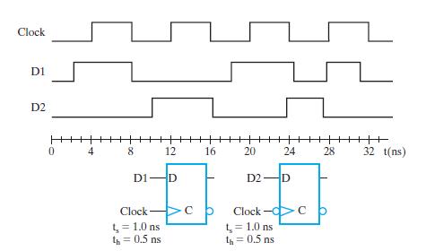
A set of waveforms applied to two D lip- lops is shown in Figure 4-56. These waveforms are applied to the lip- lops shown along with the values of their timing parameters.Figure 4-56(a) List the time(s) at which there are timing violations in signal D1 for lip- lop 2.(b) List the time(s) at which
Write a Verilog description for the state- machine diagram for the jawbreaker vending machine derived in Problem 4-38. You may obtain the state- machine diagram by either solving Problem 4-38 or inding its solution on the textbook website. In the parameter statement use a one- hot state
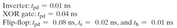
A sequential circuit is shown in Figure 4-49. The timing parameters for the gates and lip- lops are as follows:Figure 4-49:(a) Find the longest path delay from an external circuit input passing through gates only to an external circuit output.b) Find the longest path delay in the circuit from an
Repeat Problem 4-59, assuming that the circuit consists of two copies of the circuit in Figure 4-49 with input X of the second circuit copy driven by output Y of the first circuit copy.Problem 4-59A sequential circuit is shown in Figure 4-49. The timing parameters for the gates and lip- lops are as
Write a gate- level HDL description of the circuit from Problem 4-59 including delays for each component. Show that the circuit operates incorrectly when operated at a frequency greater than the maximum frequency you found as your answer for Problem 4-59. Problem 4-59A sequential circuit is shown
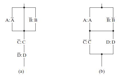
Find the Boolean function that corresponds to the closed paths through each of the given switch model networks in Figure 5-14.Figure 5-14 A: A C: C D:D (a) B: B A: A C: C (b) B: B D: D
Find the CMOS switch model networks for the following functions:(a) 3-input NAND gate.(b) 4-input NOR gate.
An integrated circuit logic family has NAND gates with a fan- out of eight standard loads and buffers with a fan- out of 16 standard loads. Sketch a schematic showing how the output signal of a single NAND gate can be applied to 38 other gate inputs, using as few buffers as possible. Assume that
(a) Given a 256 х 8 ROM chip with an enable input, show the external connections necessary to construct a 1K х 16 ROM with eight chips and a decoder.(b) How many 256 х 8 ROM chips would be required to construct a 4K х 32 ROM?
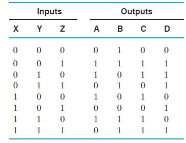
Tabulate the truth table for an 8 х 3 ROM that implements the following four Boolean functions: A(X,Y,Z) = m(0,6,7) B(X,Y,Z) = m(1,2,3,4,5)
A 32 х 8 ROM converts a 6-bit binary number to its corresponding two-digit BCD number. For example, binary 100001 converts to BCD 0011 0011 (decimal 33). Specify the truth table for the ROM.
Obtain the PLA equations for programming the four Boolean functions listed in Problem 5–7. Minimize the number of product terms. Be sure to attempt to share product terms between functions that are not prime implicants of individual functions and to consider the use of complemented
Specify the size of a ROM (number of words and number of bits per word)that will accommodate the truth table for the following combinational circuit components:(a) A 16-bit ripple carry adder with Cin and Cout.(b) An 8-bit adder– subtractor with Cin and Cout.(c) A code converter from a 4-digit
The following is the truth table of a three- input, four- output combinational circuit. Obtain the equations for programming the PAL device shown in Figure 5-10.Figure 5-10 X 0 0 0 0 1 1 1 1 Inputs Y Z 0 0 1 1 0 0 1 1 0 1 0 1 0 1 0 1 A B 0 1 1 0 1 Outputs C 0 1 0 1 1 0 1 0 0 1 1 D 0 0 1 1 1 1 0 1 1
Derive the PLA equations for the combinational circuit that squares a 3-bit number. Minimize the number of product terms. If necessary to reduce product terms, share product terms between functions that are not prime implicants of individual functions and consider the use of complemented outputs.
List the PLA equations for programming a BCD–to–excess-3 code converter. If necessary to reduce product terms, share product terms between functions that are not prime implicants of individual functions and consider the use of complemented outputs.
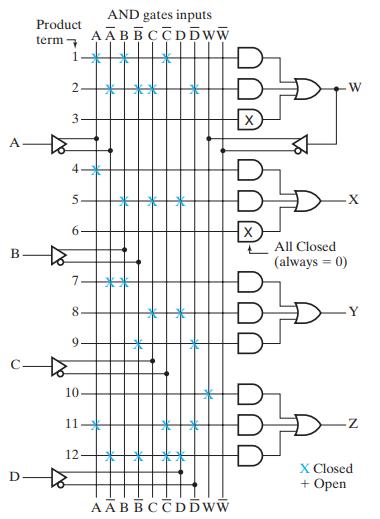
The following equations are to be implemented in the PAL device shown in Figure 5-10. Find the equations for programming the PAL.Figure 5-10 F = AB + CD + ABCD + ABC + ABCD G = AB + BCD + BCD + ABC
Repeat Problem 5-10, using a PAL device.Problem 5-10List the PLA equations for programming a BCD–to–excess-3 code converter. If necessary to reduce product terms, share product terms between functions that are not prime implicants of individual functions and consider the use of complemented
Use Shannon’s expansion theorem to express the following functions in terms of C and C̅. (a) F(A,B,C) (b) F(A,B,C) = AB + BC + AC = m(0,2,3,5,6)
Showing 100 - 200
of 439
1
2
3
4
5
Step by Step Answers
![// 4-bit Adder: Behavioral Verilog Description module adder_4_b_v (A, B, CO, S, C4); input [3:0] A, B; input](https://dsd5zvtm8ll6.cloudfront.net/images/question_images/1704/4/5/9/0846597fb4ce3c741704459084682.jpg)
![//4-bit Adder: Behavioral Verilog Description module adder_4_b_v (A, B, CO, S, C4); input [3:0] A, B; input](https://dsd5zvtm8ll6.cloudfront.net/images/question_images/1704/4/5/8/9836597fae7647951704458983141.jpg)

![0/0 or 1/1 0/1 B2=0] 0/0 or 1/1 B3 = X B3=0 0/1 (B1=0) 0/1 1/0 0/1 Init B2 = 1 (d) 1/0 1/0 B1 = 1 0/1 or 1/1](https://dsd5zvtm8ll6.cloudfront.net/images/question_images/1704/4/6/6/390659817d649d421704466389860.jpg)