New Semester
Started
Get
50% OFF
Study Help!
--h --m --s
Claim Now
Question Answers
Textbooks
Find textbooks, questions and answers
Oops, something went wrong!
Change your search query and then try again
S
Books
FREE
Study Help
Expert Questions
Accounting
General Management
Mathematics
Finance
Organizational Behaviour
Law
Physics
Operating System
Management Leadership
Sociology
Programming
Marketing
Database
Computer Network
Economics
Textbooks Solutions
Accounting
Managerial Accounting
Management Leadership
Cost Accounting
Statistics
Business Law
Corporate Finance
Finance
Economics
Auditing
Tutors
Online Tutors
Find a Tutor
Hire a Tutor
Become a Tutor
AI Tutor
AI Study Planner
NEW
Sell Books
Search
Search
Sign In
Register
study help
computer science
logic and computer design fundamentals
Logic And Computer Design Fundamentals 5th Edition M. Morris Mano, Charles Kime, Tom Martin - Solutions
For the programmable logic block shown in Figure 5-13, show the necessary configuration settings to implement each of the following types of circuits. You can assume that the upper data input of each multiplexer is chosen with a select input of 0.(a) A combinational function of inputs a, b, and
Implement the Moore state machine described by the following state table using the programmable logic block shown in Figure 5-13. Your answer should include the coniguration bits for the logic block.Figure 5-13 Present State in1 State0 State0 State0 State0 Statel Statel Statel Statel 0 0 1 1 0 0 1
(a) Design a 4-LUT using only 2-LUTs and 2-to-1 multiplexers.(b) Implement the function F = AB + C̅D + AB̅C + A̅BCD + AB̅C̅D̅ using the 4-LUT from (a).
For the programmable logic block shown in Figure 5-13, what functions should be entered into the 2-LUTs to implement a 1-bit 2s complement subtractor performing the operation a - b?Figure 5-13 b 2-LUT 1 2 2-LUT MUX2 18 MUXI carry_in sum addition logic carry_out MUX3 DQ clock www MUX4 out 10
Assume that registers R1 and R2 in Figure 6-6 hold two unsigned numbers. When select input X is equal to 1, the adder–subtractor circuit performs the arithmetic operation “R1 + 2s complement of R2.” This sum and the output carry Cn are transferred into R1 and C when K1 = 1 and a positive edge
Perform the bitwise logic AND, OR, and XOR of the two 8-bit operands 10011001 and 11000011.
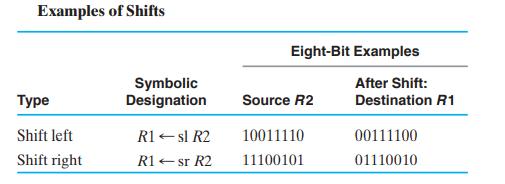
Starting from the 8-bit operand 11001010, show the values obtained after applying each shift microoperation given in Table 6-5.Table 6-5 Examples of Shifts Type Shift left Shift right Symbolic Designation R1 sl R2 R1-sr R2 Eight-Bit Examples After Shift: Destination R1 Source R2 10011110 11100101
Given the 16-bit operand 10101100 01010011, what operation must be performed and what operand must be used:(a) Clear all odd bit positions to 0? (Assume bit positions are 15 through 0 from left to right.)(b) Set the rightmost 4 bits to 1?(c) Complement the most signiicant 8 bits?
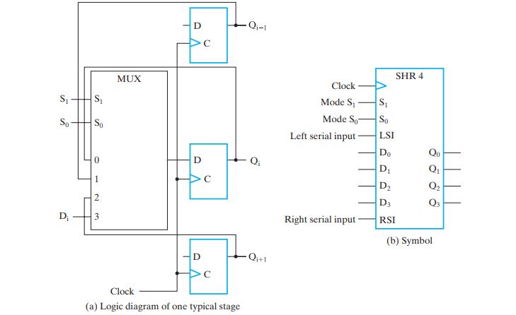
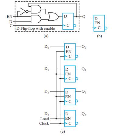
Modify the register of Figure 6-11 so that it will operate according to the following function table, using mode selection inputs S1 and S0:Figure 6-11 S So D S So 0 - 2 3 MUX D D D C Clock (a) Logic diagram of one typical stage -Q-1 -Q+1 Clock Mode S Mode So Left serial input- Right serial
A switch-tail counter (also called twisted ring counter, Johnson counter) uses the complement of the serial output of a right shift register as its serial input.(a) Starting from an initial state of 000, list the sequence of states after each shift until the register returns to 000.(b) Beginning
How many lip-lop values are complemented in an 8-bit binary ripple counter to reach the next count value after:(a) 11111111?(b) 01100111?(c) 01010110
For the CMOS logic family, the power consumption is proportional to the sum of the changes from 1-to-0 and 0-to-1 on all gate inputs and outputs in the circuit. When designing counters in very low-power circuits, ripple counters are preferred over regular synchronous binary counters. Carefully
(a) Construct a 4-bit up/down counter that uses a Gray-code counting sequence.(b) Repeat Problem 6-9 by comparing the numbers of changing inputs and outputs on the Gray-code counter to a 4-bit regular synchronous binary counter and a 4-bit ripple counter.Problem 6-9For the CMOS logic family, the
Construct a 16-bit serial-parallel counter, using four 4-bit parallel counters. Suppose that all added logic is AND gates and that serial connections are employed between the four counters. What is the maximum number of AND gates in a chain that a signal must propagate through in the 16-bit counter?
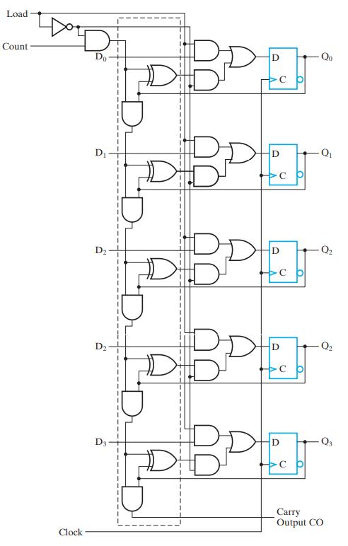
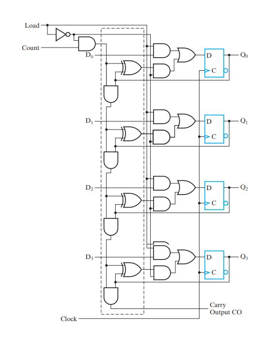
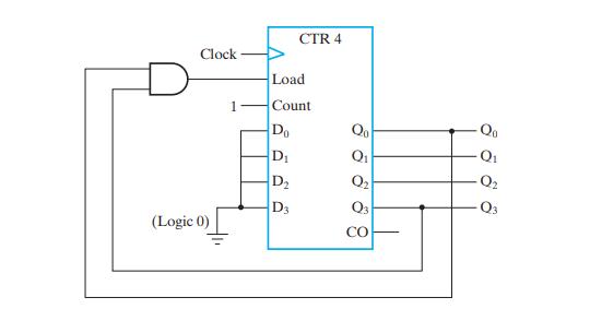
Using two binary counters of the type shown in Figure 6-14 and logic gates, construct a binary counter that counts from decimal 11 through decimal 233. Also, add an additional input and logic to the counter to initialize it synchronously to 11 when the signal INIT is 1. Figure 6-14 Load Count D Do
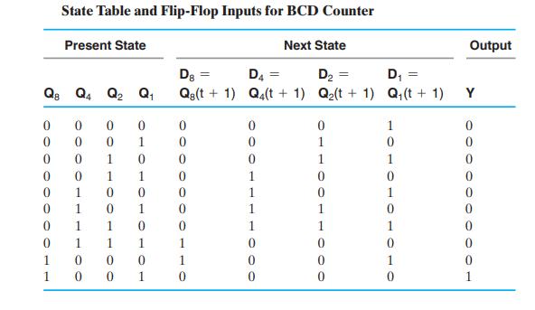
Verify the lip-lop input equations of the synchronous BCD counter specified in Table 6-9. Draw the logic diagram of the BCD counter with a count enable input.Table 6-9 0 0 Qs Q Q2 Q 8 0 0 0 0 0 State Table and Flip-Flop Inputs for BCD Counter 0 1 1 Present State 0 OOOO 0 0 0 0 0 1 0 1 1 0 1 0 1 1 0
(a) Using the synchronous binary counter of Figure 6-14 and an AND gate, construct a counter that counts from 0000 through 1010.(b) Repeat for a count from 0000 to 1110. Minimize the number of inputs to the AND gate.
Use D lip-lops and gates to design a binary counter with each of the following repeated binary sequences:(a) 0, 1, 2(b) 0, 1, 2, 3, 4, 5
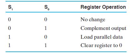
Draw the logic diagram of a 4-bit register with mode selection inputs S1 and S0. The register is to be operated according to the function table below. S 0 0 1 1 So 0 0 1 0 1 Register Operation No change Complement output Load parallel data Clear register to 0
Use D-type flip-flops and gates to design a counter with the following repeated binary sequence: 0, 2, 1, 3, 4, 6, 5, 7.
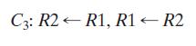
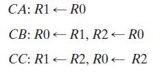
Show the diagram of the hardware that implements the register transfer statement C3: R2R1, R1 R2
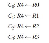
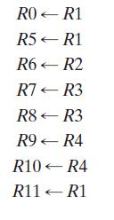
The outputs of registers R0, R1, R2, and R3 are connected through 4-to-1 multiplexers to the inputs of a ifth register, R4. Each register is 8 bits long. The required transfers, as dictated by four control variables, areThe control variables are mutually exclusive (i.e., only one variable can be
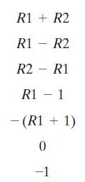
Using two 4-bit registers R1 and R2, a 4-bit adder, a 2-to-1 multiplexer, and a 4-to-1 multiplexer, construct a circuit that implements the following operations under the control of the three multiplexer select inputs and the adder’s carry-in input: R1 + R2 R1 - R2 R2 - R1 R1 1 - (R1 + 1) 0 -1
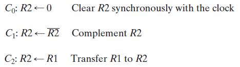
Using two 4-bit registers R1 and R2, and AND gates, OR gates, and inverters, draw one bit slice of the logic diagram that implements all of the following statements:The control variables are mutually exclusive (i.e., only one variable can be equal to 1 at any time) while the other two are equal to
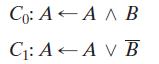
A register cell is to be designed for an 8-bit register A that has the following register transfer functions:Find optimum logic using AND, OR, and NOT gates for the D input to the D lip-lop in the cell. C: A - C: A AV B
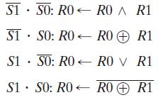
A register cell is to be designed for an 8-bit register R0 that has the following register transfer functions:Find optimum logic using AND, OR, and NOT gates for the D input to the D lip-lop in the cell. S1 S1 SO: RORO ^ R1 SO: RO R0 R1 S1 SO: RORO V R1 S1 SO: RORO + R1 .
Two register transfer statements are given (otherwise, R1 is unchanged):(a) Using a 4-bit counter with parallel load as in Figure 6-14 and a 4-bit adder as in Figure 4-5, draw the logic diagram that implements these register transfers.(b) Repeat part (a) using a 4-bit adder as in Figure 3-43 plus
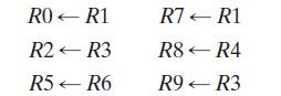
Logic to implement transfers among three registers, R0, R1, and R2, is to be implemented. Use the control variable assumptions given in Problem 6–20. The register transfers are as follows:Using registers and dedicated multiplexers, draw a detailed logic diagram of the hardware that implements a
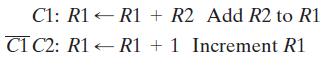
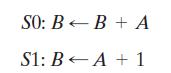
A register cell is to be designed for register B, which has the following register transfers:Share the combinational logic between the two transfers as much as possible. SO: BB+ A S1: B A + 1
Repeat Problem 6-26 using one multiplexer-based bus and one direct connection from one register to another instead of dedicated multiplexers.Problem 6-26Logic to implement transfers among three registers, R0, R1, and R2, is to be implemented. Use the control variable assumptions given in Problem
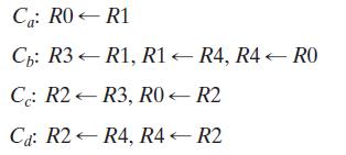
A system is to have the following set of register transfers, implemented using buses:(a) For each destination register, list all of the source registers.(b) For each source register, list all of the destination registers.(c) With consideration for which of the transfers must occur
(a) Implement function H = X̅Y + XZ using two three-state buffers and an inverter.(b) Construct an exclusive-OR gate by interconnecting two three-state buffers and two inverters.
The following register transfers are to be executed in, at most, two clock cycles: (a) What is the minimum number of buses required? Assume that only one bus can be attached to a register input and that any net connected to a register input is counted as a bus.(b) Draw a block diagram
What is the minimum number of clock cycles required to perform the following set of register transfers using one bus?Assume that only one bus can be attached to a register input and that any net connected to a register input is counted as a bus. RO < R1 R2 R3 R5 R6 R7 - R1 R8 R4 R9 R3
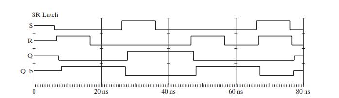
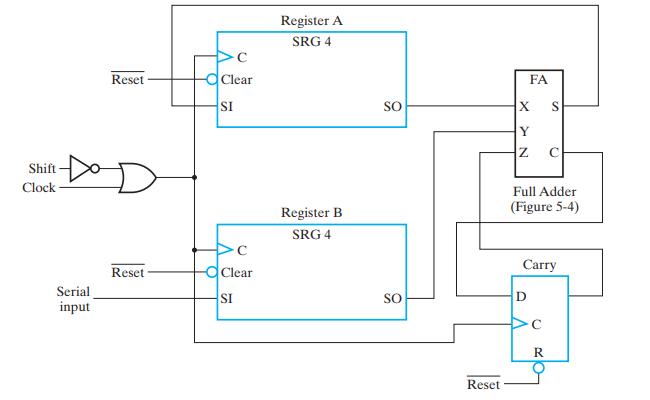
The serial adder of Figure 6-24 uses two 4-bit registers. Register A holds the binary number 0111 and register B holds 0101. The carry lip-lop is initially reset to 0. List the binary values in register A and the carry lip-lop after each of four shifts.Figure 6-24 Shift Clock Serial input Reset
The content of a 4-bit register is initially 0101. The register is shifted eight times to the right, with the sequence 10110001 as the serial input. The leftmost bit of the sequence is applied first. What is the content of the register after each shift?
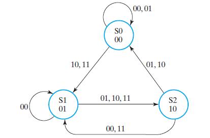
A state diagram of a sequential circuit is given in Figure 6-37. Find the corresponding state machine diagram using a minimum amount of notation. The inputs to the circuit are X1 and X2, and the outputs are Z1 and Z2.Figure 6-37 00 S1 01 10, 11 SO 00 01, 10, 11 00, 11 00, 01 01, 10 S2 10
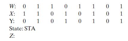
Find the response for the state machine diagram in Figure 6-38 to the following sequence of inputs (assume that the initial state is STA):Figure 6-38 W: 0 X: 1 Y: 0 State: STA Z: 1 1 1 1 0 0 0 0 1 1 1 1 1 0 1 0 0 1 0 0 0 1 1 1
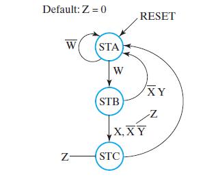
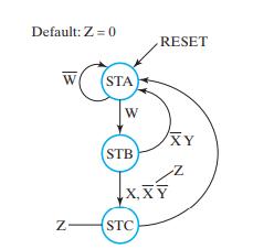
A state machine diagram is given in Figure 6-38. Find the state table for the corresponding sequential circuit.Figure 6-38 Default: Z = 0 W Z- STA W STB RESET X, XY STC XY Z
Find the state machine diagram corresponding to the following description: There are two states, A and B. If in state A and input X is 1, then the next state is A. If in state A and input X is 0, then the next state is B. If in state B and input Y is 0, then the next state is B. If in state B and
Find the state machine diagram for a circuit that detects a difference in value in an input signal X at two successive positive clock edges. If X has different values at two successive positive clock edges, then output Z is equal to 1 for the next clock cycle. Otherwise, output Z is 0.
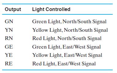
Find a state machine diagram for a trafic light controller that works as follows: A timing signal T is the input to the controller. T deines the yellow light interval, as well as the changes of the red and green lights. The outputs to the signals are deined by the following table:While T = 0, the
Implement the state machine diagram in Figure 6-38 by using one lip-lop per state assignment.Figure 6-38 Default: Z=0 W N (STA) W RESET (STB) X,XY (STC) XY
The state machine diagram for a synchronous circuit with clock CK for a washing machine is to be developed. The circuit has three external inputs, START, FULL, and EMPTY (which are 1 for at most a single clock cycle and are mutually exclusive), and external outputs, HOT, COLD, DRAIN, and TURN. The
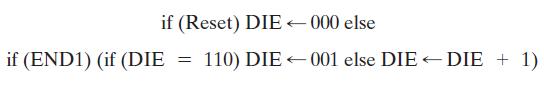
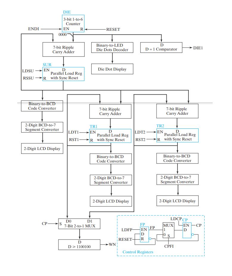
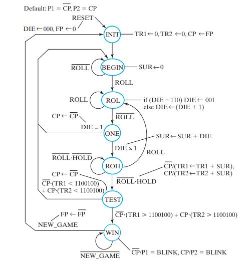
Do two designs for the DIE circuit for the Game of PIG and compare the gate-input costs of your two designs using information from Figure 6-14. Note that the register transfer description of DIE is:Figure 6-14.(a) Perform the design by using the technique given for the BCD counter design in Figure
Design the following combinational circuits for the Game of PIG datapath given in Figure 6-31:Figure 6-31(a) D = 1 comparator.(b) D ≥ 1100100 comparator.Use AND gates, OR gates, and inverters. Assume the maximum gate fan-in is four. ENDI SUR LDSU- Binary-to-BCD Code Converter 0000 7-bit Ripple
Implement the state machine diagram derived in Problem 6-40 by using a Gray-code state assignment.Problem 6-40Find the state machine diagram for a circuit that detects a difference in value in an input signal X at two successive positive clock edges. If X has different values at two successive
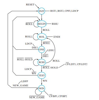
(a) Show the details of a check of the constraints given on transition conditions as applied to Figure 6-30.(b) Implement the state machine diagram for the Game of PIG in Figure 6-30 using a one-hot state assignment D lip-lops, and gates.Figure 6-30 RESET ROLL ROLL LDCP ROLL HOLD LDCP LDFP NEW
Find the state machine diagram in the form of Figure 6-29 for a Game of PIG using two dice. Also, add the following rule: If a pair of 1s is rolled, then the player’s total score becomes 0. The two dice create an interesting problem: How do you make sure that the values rolled on the two dice
Design the 2-digit binary-to-BCD code converter in the datapath for the Game of PIG. Design the least significant digit as a function of (B3, B2, B1, B0)without an incoming carry C0. The outputs are to be C4, D3, D2, D1, D0. Design the same circuit with an incoming carry C0 ixed to 1. For the most
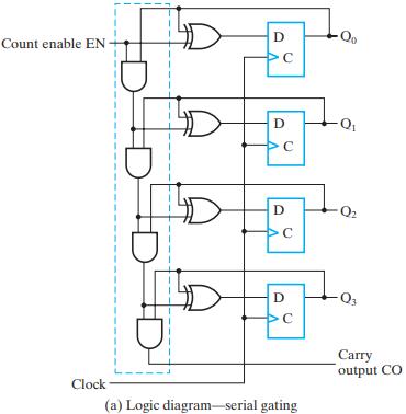
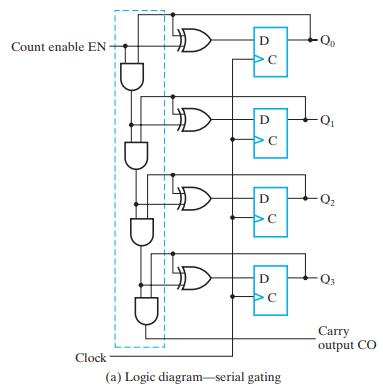
Write a Verilog description for the 4-bit binary counter in Figure 6-13(a) using a register for the D lip-lops and Boolean equations for the logic. Compile and simulate your description to demonstrate correctness.Figure 6-13(a) Count enable EN- Clock D D C D C D C (a) Logic diagram-serial gating
Design a digital system with three 16-bit registers AR, BR, and CR and 16-bit data input IN to perform the following operations, assuming a 2s complement representation and ignoring overlow:(a) Transfer two 16-bit signed numbers to AR and BR on successive clock cycles after a go signal G becomes
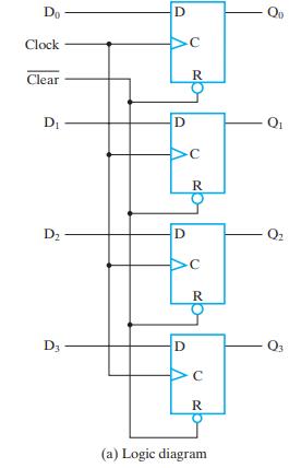
Write a behavioral VHDL description for the 4-bit register in Figure 6-1(a). Compile and simulate your description to demonstrate correctness.Figure 6-1(a). Do Clock Clear D D D3 D D D D C R R R C RP (a) Logic diagram Qo Q 9 03
Repeat Problem 6-52 for the 4-bit register with parallel load in Figure 6-2.Figure 6-2Problem 6-52Write a behavioral VHDL description for the 4-bit register in Figure 6-1(a). Compile and simulate your description to demonstrate correctness.Figure 6-1(a). B ID Flip-flop with enable (a) D+ C+ Do D D-
Write a VHDL description for the 4-bit binary counter in Figure 6-13(a), using a register for the D lip-lops and Boolean equations for the logic. Compile and simulate your description to demonstrate correctness.Figure 6-13(a) Count enable EN Clock 1 1 1 1 I 1 1 1 1 1 I D 5 D C D C D C D DC (a)
Repeat Problem 6-55 for the 4-bit register with parallel load in Figure 6-2.Figure 6-2Problem 6-55Write a behavioral Verilog description for the 4-bit register in Figure 6-1(a). Compile and simulate your description to demonstrate correctness.Figure 6-1(a). B ID Flip-flop with enable (a) D+ C+ Do D
Write a behavioral Verilog description for the 4-bit register in Figure 6-1(a). Compile and simulate your description to demonstrate correctness.Figure 6-1(a). Do Clock Clear D D D3 D D D D C R R R C RP (a) Logic diagram Qo Q 9 03
Write, compile, and simulate a VHDL description for the state machine diagram shown in Figure 6-38. Use a simulation input that passes through all paths in the state machine diagram, and include both the state and output Z as simulation outputs. Correct and resimulate your design if
Write, compile, and simulate a Verilog description for the state machine diagram in Figure 6-38. Use code 00 for state STA, 01 for state STB, and 10 for state STC. Use a simulation input that passes through all paths in the state-machine diagram and include both the state and Z as simulation
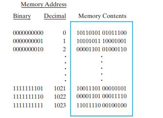
a) Word number (835)10 in the memory shown in Figure 7-2 contains the binary equivalent of (15,103)10. List the 10-bit address and the 16-bit memory contents of the word.(b) Repeat part (a) for word number (513)10 containing the binary equivalent of (44,252)10.Figure 7-2 Memory Address Binary
The following memories are specified by the number of words times the number of bits per word. How many address lines and input–output data lines are needed in each case?(a) 48K х 8,(b) 512K х 32,(c) 64M х 64, and(d) 2G х 1.
A 64K х 16 RAM chip uses coincident decoding by splitting the internal decoder into row select and column select.(a) Assuming that the RAM cell array is square, what is the size of each decoder, and how many AND gates are required for decoding an address?(b) Determine the row and column
Assume that the largest decoder that can be used in an m х 1 RAM chip has 14 address inputs and that coincident decoding is employed. In order to construct RAM chips that contain more one-bit words than m, multiple RAM cell arrays, each with decoders and read/write circuits, are included in the
A DRAM has 15 address pins and its row address is 1 bit longer than its column address. How many addresses, total, does the DRAM have?
A 4 GB DRAM uses 4-bit data and has equal-length row and column addresses. How many address pins does the DRAM have?
A DRAM has a refresh interval of 64 ms and has 8192 rows. What is the interval between refreshes for distributed refresh? What is the total time required out of the 64 ms for a refresh of the entire DRAM? What is the minimum number of address pins on the DRAM?
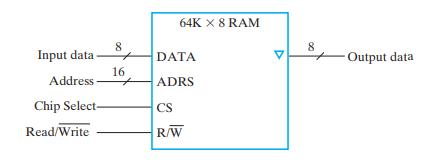
Using the 64K х 8 RAM chip in Figure 7-9 plus a decoder, construct the block diagram for a 1M х 32 RAM.Figure 7-9 Input data- Address Chip Select- Read/Write 8 16 + 64K X 8 RAM DATA ADRS CS R/W 8 Output data
(a) How many 128K х 16 RAM chips are needed to provide a memory capacity of 2 MB?(b) How many address lines are required to access 2 MB? How many of these lines are connected to the address inputs of all chips?(c) How many lines must be decoded to produce the chip select inputs? Specify the
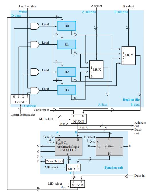
A datapath similar to the one in Figure 8-1 has 64 registers. How many selection lines are needed for each set of multiplexers and for the decoder?Figure 8-1 Load enable Write D data 0123 Decoder D address Load Destination select Load Load Load Constant in- MB select n V4 C+ N Z A RO Zero Detect MF
Explain how SDRAM takes advantage of the two-dimensional storage array to provide a high data access rate.
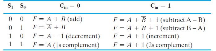
Design an arithmetic circuit with two selection variables S1 and S0 and two n- bit data inputs A and B. The circuit generates the following eight arithmetic operations in conjunction with carry Cin:Draw the logic diagram for the two least significant bits of the arithmetic circuit. S So 0 0 0 1 1
Given an 8-bit ALU with outputs F7 through F0 and available carries C8 and C7, show the logic circuit for generating the signals for the four status bits N (sign), Z (zero), V (overflow), and C (carry).
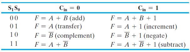
Design a 4-bit arithmetic circuit, with two selection variables S1 and S0, that generates the arithmetic operations in the following table. Draw the logic diagram for a typical single- bit stage and the LSB stage. S So 00 01 10 11 Cin = 0 F = A + B (add) F = A (transfer) F = B (complement) F = A +
Inputs Xi and Yi of each full adder in an arithmetic circuit have digital logic specified by the Boolean functionswhere S is a selection variable, Cin is the input carry, and Ai and B i are input data for stage i.(a) Draw the logic diagram for the 4-bit circuit, using full adders and
Design an ALU that performs the following operations:Give the result of your design as the logic diagram for a single stage of the ALU. Your design should have one carry line to the left and one carry line to the right between stages and three selection bits. If you have access to logic
Design one bit of a digital circuit that performs the four logic operations of exclusive- OR, exclusive- NOR, NOR, and NAND on register operands A and B with the result to be loaded into register A. Use two selection variables.(a) Using a Karnaugh map, design minimum logic for one typical stage,
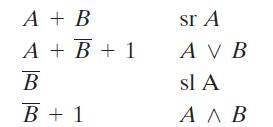
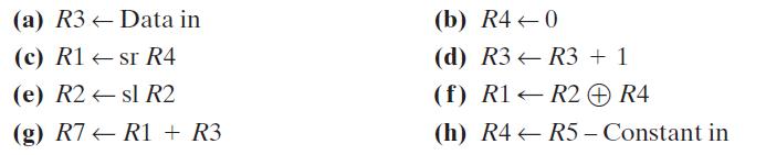
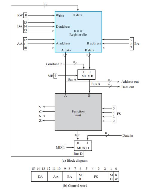
Specify the 16-bit control word that must be applied to the datapath of Figure 8-11 to implement each of the following microoperations:Figure 8-11 Data in sr R4 sl R2 (a) R3 (c) R1 (e) R2 (g) R7R1 + R3 (b) R40 (d) R3 R3 + 1 (f) R1 R2 R4 (h) R4R5 - Constant in
Given the sequence of 16-bit control words below for the datapath in Figure 8-11 and the initial ASCII character codes in 8-bit registers, simulate the datapath to determine the alphanumeric characters in the registers after the execution of the sequence. The result is a scrambled word: what is
Find the output Y of the 4-bit barrel shifter in Figure 8-9 for each of the following bit patterns applied to S1, S0, D3, D2, D1, and D0:(a) 110101(b) 101011(c) 011010(d) 001101
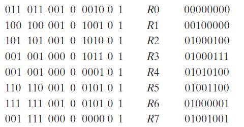
Given the following 16-bit control words for the datapath of Figure 8-11, determine (a) the microoperation that is executed and (b) the change in the contents of the register for each control word (assume that the registers are 8-bit registers and that, before the execution of a control word,
The single- cycle computer in Figure 8-15 executes the ive instructions described by the register transfers in the table that follows.Figure 8-15(a) Complete the following table, giving the binary instruction decoder outputs from Figure 8-16 during execution of each of the instructions:Figure
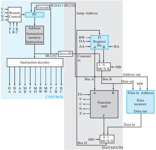
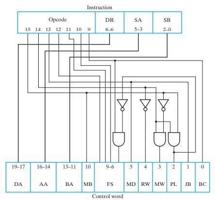
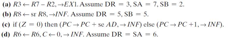
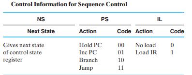
List the control logic state table entries for the multiple- cycle computer (see Tables 8-12, 8-13 and 8-15) that implement the following register transfer statements. Assume that in all cases the present state is EX0. If an opcode is needed, use a symbolic name based on the problem part— e.g.,
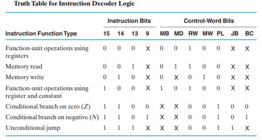
Using the information in the truth table in Table 8-10, verify that the design for the single- bit outputs in the decoder in Figure 8-16 is correct.Table 8-10Figure 8-16 Truth Table for Instruction Decoder Logic Instruction Function Type Function-unit operations using registers Memory read Memory
A computer has a 32-bit instruction word broken into ields as follows:opcode, six bits; two register ile address ields, ive bits each; and one immediate operand/register ile address ield, 16 bits.(a) What is the maximum number of operations that can be speciied?(b) How many registers can be
Manually simulate the single- cycle computer in Figure 8-15 for the following sequence of instructions, assuming that each register initially contains contents equal to its index (i.e., R0 contains 0, R1 contains 1, and so on):Figure 8-15Give (a) the binary value of the instruction on the current
A digital computer has a memory unit with a 32-bit instruction and a register file with 64 registers. The instruction set consists of 130 different operations. There is only one type of instruction format, with an opcode part, a register ile address, and an immediate operand part. Each instruction
A digital computer has 32-bit instructions. There are a number of different instruction formats, and the number of bits in each format used for opcodes varies depending on the bits needed for other fields. If the first bit of the opcode is 0, then there are three opcode bits. If the first bit of
Give an instruction for the single- cycle computer that resets register R4 to 0 and updates the Z and N status bits based on the value 0 transferred to R4.By examining the detailed ALU logic, determine the values of the V and C status bits.
a) Manually simulate the SRM (shift right multiple) instruction in the multiple- cycle computer for operand 0101100111000111 for OP = 5.(b) Repeat part (a) for the SLM (shift left multiple) instruction.
Repeat Problem 8-22 for the two instructions: Add and check OV (AOV), described by the register transferand branch on overlow (BRV), described by the register transferThe opcode for AOV is 1000101 and for BRV is 1000110. Note that register R8 is used as a “status” register that stores the
A new instruction is to be deined for the multiple- cycle computer with opcode 0010001. The instruction implements the register transferFind the state machine diagram for implementing the instruction, assuming that 0010001 is the opcode. Form the part of the control state table that implements this
In the SRM and SLM instructions, both the operand R[SA] and the shift amount ield OP are checked to see if either is 0 before the shifts begin.(a) Redraw the state machine diagram for these operations with these checks removed.(b) Use the original diagram and the new diagram to compare the number
A new instruction, SMR (Store Multiple Registers), with symbolic opcode name SMR, is to be implemented for the multiple- cycle computer. The instruction stores the contents of eight registers in eight consecutive memory locations. Register R[SA] specifies the address in memory M to which the
A new instruction is to be defined for the multiple- cycle computer. The instruction compares two unsigned integers stored in register R[SA] and R[SB]. If the integers are equal, then bit 0 of R[DR] is set to 1. If R[SA] is greater than R[SB], then bit 1 of R[DR] is set to 1. Otherwise, bits 0 and
A new instruction, ANDN (AND NOT), is to be implemented for the multiple-cycle computer. The instruction performs R[DR] = R[SA]^(NOT(R[SB])). The instruction allows individual bits in register SA to be cleared based upon a mask stored in SB, where the bit to be cleared is a 1 in the mask value.
A program is to be written for a stack architecture for the arithmetic expression(a) Find the corresponding RPN expression.(b) Write the program using PUSH, POP, ADD, MUL, SUB, and DIV instructions as appropriate for the operators in the expression.(c) Show the contents of the stack after the
Repeat Problem 9-3 for the arithmetic expressionProblem 9-3A program is to be written for a stack architecture for the arithmetic expression(a) Find the corresponding RPN expression.(b) Write the program using PUSH, POP, ADD, MUL, SUB, and DIV instructions as appropriate for the operators in the
Using the instructions for the single- cycle computer, write a program that reads through an array of 16-bit signed 2s complement numbers stored in data memory and finds the minimum value in the array. Your program must read the address of the start of the array (i.e., a pointer to the array) from
A two- word relative mode branch- type instruction is stored in memory at locations 207 and 208 (decimal). The branch is made to an address equivalent to decimal 195. Let the address field of the instruction (stored at address 208) be designated by X.(a) Determine the value of X in
Repeat Problem 9-6 for a branch instruction in locations 143 and 144 and a branch address equivalent to 1000. All values are in decimal.Problem 9-6A two- word relative mode branch- type instruction is stored in memory at locations 207 and 208 (decimal). The branch is made to an address equivalent
Showing 200 - 300
of 439
1
2
3
4
5
Step by Step Answers

![Instruction Register Transfer R[0] R[7] R[3] R[1] M[R[4]] R[2] R[5]+2 R[3] sl R[6] if (R([4] = 0) PC](https://dsd5zvtm8ll6.cloudfront.net/images/question_images/1704/5/6/8/2286599a5a42333e1704568225237.jpg)
![Control-Word Information for Datapath DX AX BX Code MB Code FS R[DR] R[SA] R[SB] OXXX Register 0 F = A R8 R8](https://dsd5zvtm8ll6.cloudfront.net/images/question_images/1704/5/6/8/5726599a6fc9e2ec1704568570419.jpg)
![R[DR] R[SB] + M[R[SA]]](https://dsd5zvtm8ll6.cloudfront.net/images/question_images/1704/5/6/8/6946599a776cd8591704568693070.jpg)