New Semester
Started
Get
50% OFF
Study Help!
--h --m --s
Claim Now
Question Answers
Textbooks
Find textbooks, questions and answers
Oops, something went wrong!
Change your search query and then try again
S
Books
FREE
Study Help
Expert Questions
Accounting
General Management
Mathematics
Finance
Organizational Behaviour
Law
Physics
Operating System
Management Leadership
Sociology
Programming
Marketing
Database
Computer Network
Economics
Textbooks Solutions
Accounting
Managerial Accounting
Management Leadership
Cost Accounting
Statistics
Business Law
Corporate Finance
Finance
Economics
Auditing
Tutors
Online Tutors
Find a Tutor
Hire a Tutor
Become a Tutor
AI Tutor
AI Study Planner
NEW
Sell Books
Search
Search
Sign In
Register
study help
computer science
digital design computer
Digital Design and Computer Architecture 2nd edition David Harris, Sarah Harris - Solutions
You are walking down the hallway when you run into your lab partner walking in the other direction. The two of you first step one way and are still in each other’s way. Then you both step the other way and are still in each other’s way. Then you both wait a bit, hoping the other person will
You would like to build a synchronizer that can receive asynchronous inputs with an MTBF of 50 years. Your system is running at 1 GHz, and you use sampling flip-flops with τ = 100 ps, T0 = 110 ps, and tsetup = 70 ps. The synchronizer receives a new asynchronous input on average 0.5 times per
A field programmable gate array (FPGA) uses configurable logic blocks (CLBs) rather than logic gates to implement combinational logic. The Xilinx Spartan 3 FPGA has propagation and contamination delays of 0.61 and 0.30 ns, respectively, for each CLB. It also contains flip-flops with propagation and
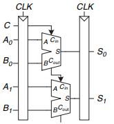
You are designing an adder for the blindingly fast 2-bit RePentium Processor. The adder is built from two full adders such that the carry out of the first adder is the carry in to the second adder, as shown in Figure 3.75. Your adder has input and output registers and must complete the addition in
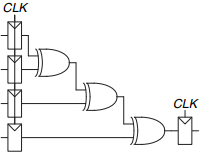
Ben Bitdiddle has designed the circuit in Figure 3.74 to compute a registered four-input XOR function. Each two-input XOR gate has a propagation delay of 100 ps and a contamination delay of 55 ps. Each flip-flop has a setup time of 60 ps, a hold time of 20 ps, a clock-to-Q maximum delay of 70 ps,
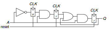
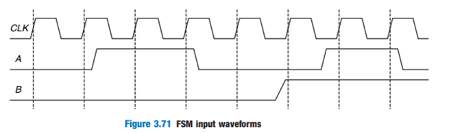
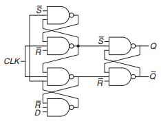
Repeat Exercise 3.31 for the FSM shown in Figure 3.73. Recall that the s and r register inputs indicate set and reset, respectively. Data From Problem 31Analyze the FSM shown in Figure 3.72. Write the state transition and output tables and sketch the state transition diagram. Describe in words
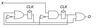
Analyze the FSM shown in Figure 3.72. Write the state transition and output tables and sketch the state transition diagram. Describe in words what the FSM does. X- CLK CLK
Design an FSM with one input, A, and two outputs, X and Y. X should be 1 if A has been 1 for at least three cycles altogether (not necessarily consecutively). Y should be 1 if A has been 1 for at least two consecutive cycles. Show your state transition diagram, encoded state transition table, next
Your company, Detect-o-rama, would like to design an FSM that takes two inputs, A and B, and generates one output, Z. The output in cycle n, Zn, is either the Boolean AND or OR of the corresponding input An and the previous input An-1, depending on the other input, Bn: Zn= An An−1 if Bn= 0 Zn= An
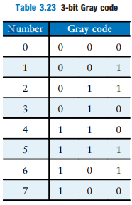
Gray codes have a useful property in that consecutive numbers differ in only a single bit position. Table 3.23 lists a 3-bit Gray code representing the numbers 0 to 7. Design a 3-bit modulo 8 Gray code counter FSM with no inputs and three outputs. (A modulo N counter counts from 0 to N − 1, then
How would you factor the FSM from Exercise 3.20 into multiple simpler machines? How many states does each simpler machine have? What is the minimum total number of bits necessary in this factored design? Data From Problem 20You are designing an FSM to keep track of the mood of four students
You are designing an FSM to keep track of the mood of four students working in the digital design lab. Each student’s mood is either HAPPY (the circuit works), SAD (the circuit blew up), BUSY (working on the circuit), CLUELESS (confused about the circuit), or ASLEEP (face down on the circuit
Design an asynchronously settable D flip-flop using logic gates.
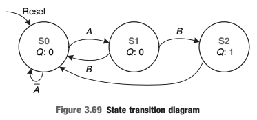
Describe in words what the state machine in Figure 3.69 does. Using binary state encodings, complete a state transition table and output table for the FSM. Write Boolean equations for the next state and output and sketch a schematic of the FSM. Reset A B so S1 S2 Q: 0 Q: 1 Q:0 в Figure 3.69
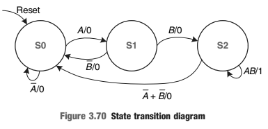
Describe in words what the state machine in Figure 3.70 does. Using binary state encodings, complete a state transition table and output table for the FSM. Write Boolean equations for the next state and output and sketch a schematic of the FSM. Reset A/0 B/O S1 S2 so B/O AB/1 A/O Ā+ BIO
Accidents are still occurring at the intersection of Academic Avenue and Bravado Boulevard. The football team is rushing into the intersection the moment light B turns green. They are colliding with sleep-deprived CS majors who stagger into the intersection just before light A turns red. Extend the
Alyssa P. Hacker’s snail has a daughter with a Mealy machine FSM brain. The daughter snail smiles whenever she slides over the pattern 1101 or the pattern 1110. Sketch the state transition diagram for this happy snail using as few states as possible. Choose state encodings and write a combined
You have been enlisted to design a soda machine dispenser for your department lounge. Sodas are partially subsidized by the student chapter of the IEEE, so they cost only 25 cents. The machine accepts nickels, dimes, and quarters. When enough coins have been inserted, it dispenses the soda and
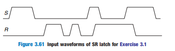
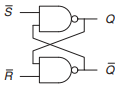
Given the input waveforms shown in Figure 3.61, sketch the output, Q, of an SR latch. л Figure 3.61 Input waveforms of SR latch for Exercise 3.1
Sketch a reasonably simple combinational circuit implementing each of the functions from Exercise 2.6.
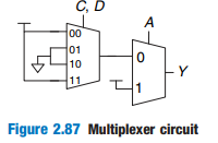
Write a minimized Boolean equation for the function performed by the circuit in Figure 2.87. C, D A 00 01 10 11 Figure 2.87 Multiplexer circuit
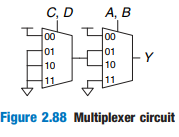
Write a minimized Boolean equation for the function performed by the circuit in Figure 2.88. C, D A, B 00 01 10 11 00 01 10 11 Figure 2.88 Multiplexer circuit
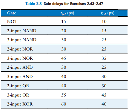
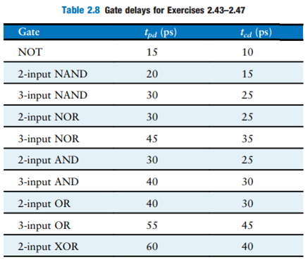
Redesign the circuit from Exercise 2.35 to be as fast as possible. Use only the gates from Table 2.8. Sketch the new circuit and indicate the critical path. What are its propagation delay and contamination delay? Table 2.8 Gate delays for Exercises 2.43–2.47 (sd) Pd, 15 Gate ted (ps) NOT 10 15
Implement the function from Figure 2.80(b) using (a) An 8:1 multiplexer(b) A 4:1 multiplexer and one inverter(c) A 2:1 multiplexer and two other logic gates B Y 1
Implement the function from Exercise 2.17(a) Using (a) an 8:1 multiplexer(b) A 4:1 multiplexer and no other gates(c) A 2:1 multiplexer, one OR gate, and an inverter
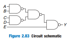
Determine the propagation delay and contamination delay of the circuit in Figure 2.83. Use the gate delays given in Table 2.8.
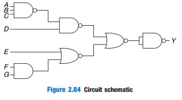
Determine the propagation delay and contamination delay of the circuit in Figure 2.84. Use the gate delays given in Table 2.8. Table 2.8 Gate delays for Exercises 2.43–2.47 (sd) Pdq 15 Gate ted (ps) NOT 10 2-input NAND 15 30 3-input NAND 25 2-input NOR 30 25 3-input NOR 45 35 2-input AND 30
Sketch a schematic for a fast 3:8 decoder. Suppose gate delays are given in Table 2.8 (and only the gates in that table are available). Design your decoder to have the shortest possible critical path, and indicate what that path is. What are its propagation delay and contamination delay? Table 2.8
Redesign the priority encoder from Exercise 2.36 to be as fast as possible. You may use any of the gates from Table 2.8. Sketch the new circuit and indicate the critical path. What are its propagation delay and contamination delay? Table 2.8 Gate delays for Exercises 2.43–2.47 (sd) Pd, 15
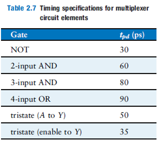
Design an 8:1 multiplexer with the shortest possible delay from the data inputs to the output. You may use any of the gates from Table 2.7 on page 92. Sketch a schematic. Using the gate delays from the table, determine this delay. Table 2.7 Timing specifications for multiplexer circuit elements
Draw a state machine that can detect when it has received the serial input sequence 01010.
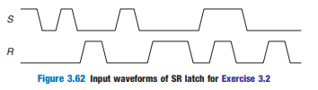
Given the input waveforms shown in Figure 3.62, sketch the output, Q, of an SR latch. Figure 3.62 Input waveforms of SR latch for Exercise 3.2
Design a serial (one bit at a time) two’s complementer FSM with two inputs, Start and A, and one output, Q. A binary number of arbitrary length is provided to input A, starting with the least significant bit. The corresponding bit of the output appears at Q on the same cycle. Start is asserted
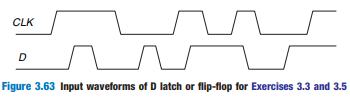
Given the input wave forms shown in Figure 3.63, sketch the output, Q, of a D latch. CLK Figure 3.63 Input waveforms of D latch or flip-flop for Exercises 3.3 and 3.5
What is the difference between a latch and a flip-flop? Under what circumstances is each one preferable?
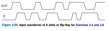
Given the input waveforms shown in Figure 3.64, sketch the output, Q, of a D latch. CLK Figure 3.64 Input waveforms of D latch or flip-flop for Exercises 3.4 and 3.6
Design a 5-bit counter finite state machine.
Given the input wave forms shown in Figure 3.63, sketch the output, Q, of a D flip-flop. CLK D
Design an edge detector circuit. The output should go HIGH for one cycle after the input makes a 0 → 1 transition.
Given the input wave forms shown in Figure 3.64, sketch the output, Q, of a D flip-flop. CLK D
Describe the concept of pipelining and why it is used.
Is the circuit in Figure 3.65 combinational logic or sequential logic? Explain in a simple fashion what the relationship is between the inputs and outputs. What would you call this circuit?
Describe what it means for a flip-flop to have a negative hold time.
Is the circuit in Figure 3.66 combinational logic or sequential logic? Explain in a simple fashion what the relationship is between the inputs and outputs. What would you call this circuit? CLK
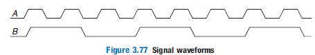
Given signal A, shown in Figure 3.77, design a circuit that produces signal B. A B Figure 3.77 Signal waveforms
The toggle (T) flip-flop has one input, CLK, and one output, Q. On each rising edge of CLK, Q toggles to the complement of its previous value. Draw a schematic for a T flip-flop using a D flip-flop and an inverter.
Consider a block of logic between two registers. Explain the timing constraints. If you add a buffer on the clock input of the receiver (the second flipflop), does the setup time constraint get better or worse?
A JK flip-flop receives a clock and two inputs, J and K. On the rising edge of the clock, it updates the output, Q. If J and K are both 0, Q retains its old value. If only J is 1, Q becomes 1. If only K is 1, Q becomes 0. If both J and K are 1, Q becomes the opposite of its present state.(a)
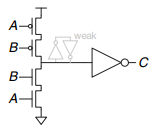
The circuit in Figure 3.67 is called a Muller C-element. Explain in a simple fashion what the relationship is between the inputs and output. A-[ B-HAY weak в- A-
Design an asynchronously resettable D latch using logic gates.
Design an asynchronously resettable D flip-flop using logic gates.
Design a synchronously settable D flip-flop using logic gates.
Suppose a ring oscillator is built from N inverters connected in a loop. Each inverter has a minimum delay of tcd and a maximum delay of tpd. If N is odd, determine the range of frequencies at which the oscillator might operate.
Which of the circuits in Figure 3.68 are synchronous sequential circuits? Explain. (a)(b)(c) (d) CLK
You are designing an elevator controller for a building with 25 floors. The controller has two inputs: UP and DOWN. It produces an output indicating the floor that the elevator is on. There is no floor 13. What is the minimum number of bits of state in the controller?
A priority encoder has 2N inputs. It produces an N-bit binary output indicating the most significant bit of the input that is TRUE, or 0 if none of the inputs are TRUE. It also produces an output NONE that is TRUE if none of the inputs are TRUE. Design an eight-input priority encoder with inputs
An M-bit thermometer code for the number k consists of k 1’s in the least significant bit positions and M – k 0’s in all the more significant bit positions. A binary-to-thermometer code converter has N inputs and 2N –1 outputs. It produces a 2N –1 bit thermometer code for the number
Design a modified priority encoder that receives an 8-bit input, A7:0, and produces two 3-bit outputs, Y2:0 and Z2:0 Y indicates the most significant bit of the input that is TRUE. Z indicates the second most significant bit of the input that is TRUE. Y should be 0 if none of the inputs are TRUE. Z
A circuit has four inputs and two outputs. The inputs Α3:0 represent a number from 0 to 15. Output P should be TRUE if the number is prime (0 and 1 are not prime, but 2, 3, 5, and so on, are prime). Output D should be TRUE if the number is divisible by 3. Give simplified Boolean equations for each
Complete the design of the seven-segment decoder segments Sc through Sg(a) Derive Boolean equations for the outputs Sc through Sg assuming that inputs greater than 9 must produce blank (0) outputs.(b) Derive Boolean equations for the outputs Sc through Sg assuming that inputs greater than 9 are
Ben Bitdiddle will enjoy his picnic on sunny days that have no ants. He will also enjoy his picnic any day he sees a hummingbird, as well as on days where there are ants and ladybugs. Write a Boolean equation for his enjoyment (E) in terms of sun (S), ants (A), hummingbirds (H), and ladybugs (L).
Sketch a circuit for the function from Exercise 2.31.
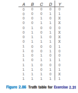
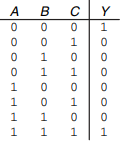
Find a minimal Boolean equation for the function in Figure 2.86. Remember to take advantage of the don’t care entries. х х х х х х Figure 2.86 Truth table for Exercise 2.31 O HOH OHOH OHOH OHOH Olo o
Does your circuit from Exercise 2.29 have any potential glitches when one of the inputs changes? If not, explain why not. If so, show how to modify the circuit to eliminate the glitches.
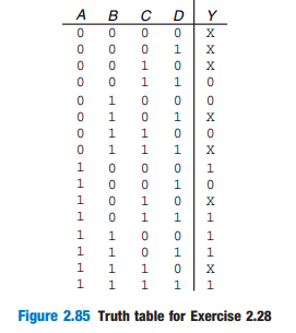
Sketch a circuit for the function from Exercise 2.28.
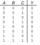
Find a minimal Boolean equation for the function in Figure 2.85. Remember to take advantage of the don’t care entries. Figure 2.85 Truth table for Exercise 2.28 Oo HO H OHOH OHOHOHOH
Repeat Exercise 2.26 for the circuit in Figure 2.84. Data From Problem 26.Using De Morgan equivalent gates and bubble pushing methods, redraw the circuit in Figure 2.83 so that you can find the Boolean equation by inspection. Write the Boolean equation. Figure 2.84 Circuit schematic A B- C-
Using De Morgan equivalent gates and bubble pushing methods, redraw the circuit in Figure 2.83 so that you can find the Boolean equation by inspection. Write the Boolean equation. B- C- D- E- Dor Figure 2.83 Circuit schematic
Minimize the Boolean equations from Exercise 2.24 and sketch an improved circuit with the same function.
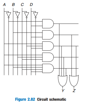
Write Boolean equations for the circuit in Figure 2.82. You need not minimize the equations. А в сD Figure 2.82 Circuit schematic
Prove De Morgan’s Theorem (T12) for three variables, B2, B1, B0, using perfect induction.
Prove that the following theorems are true using perfect induction. You need not prove their duals.(a) The idempotency theorem (T3)(b) The distributivity theorem (T8)(c) The combining theorem (T10)
Alyssa P. Hacker says that any Boolean function can be written in minimal sum-of-products form as the sum of all of the prime implicants of the function. Ben Bitdiddle says that there are some functions whose minimal equation does not involve all of the prime implicants. Explain why Alyssa is right
Give an example of a circuit with a cyclic path that is nevertheless combinational.
Give an example of a truth table requiring between 3 billion and 5 billion rows that can be constructed using fewer than 40 (but at least 1) two-input gates.
Simplify each of the following Boolean equations. Sketch a reasonably simple combinational circuit implementing the simplified equation.(a) (b)(c) Y = ABC+BC +BC Y = (A+B+C)D+AD+B
Simplify each of the following Boolean equations. Sketch a reasonably simple combinational circuit implementing the simplified equation(a) (b)(c) Y = BC+ĀBC+ BT Y = A+ĀB+AB +A+B
Sketch a reasonably simple combinational circuit implementing each of the functions from Exercise 2.14.Data From Problem 14(a) (b)(c) Y = ABC+ĀBT Y = ABC+ AB
Sketch a reasonably simple combinational circuit implementing each of the functions from Exercise 2.13.Data from Problem 13(a) (b)(c) Y = AC+ABC Y = AB+ABC+(A+T)
Simplify the following Boolean equations using Boolean theorems. Check for correctness using a truth table or K-map.(a) (b)(c) Y = ABC+ĀBT Y = ABC+ AB
Simplify the following Boolean equations using Boolean theorems. Check for correctness using a truth table or K-map.(a) (b)(c) Y = AC+ABC Y = AB+ABC+(A+T)
Repeat Exercise 2.8 using only NOT gates and NAND and NOR gates.
Repeat Exercise 2.7 using only NOT gates and NAND and NOR gates.
Repeat Exercise 2.8 using only NOT gates and AND and OR gates.
Repeat Exercise 2.7 using only NOT gates and AND and OR gates.
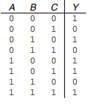
Minimize each of the Boolean equations from Exercise 2.2.Data From Problem 2Write a Boolean equation in sum-of-products canonical form for each of the truth tables in Figure 2.81.(a) (b)(c)(d)(e) A в 1 O HOH O HOH
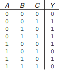
Minimize each of the Boolean equations from Exercise 2.1.Data From Problem 1Write a Boolean equation in sum-of-products canonical form for each of the truth tables in Figure 2.80.(a) (b)(c)(d)(e) A Oo HO1O1OH
Explain why a circuit’s contamination delay might be less than (instead of equal to) its propagation delay.
Write a Boolean equation in product-of-sums canonical form for the truth tables in Figure 2.81.(a) (b)(c)(d)(e) A в 1 O HOH O HOH
A gate or set of gates is universal if it can be used to construct any Boolean function. For example, the set {AND, OR, NOT} is universal.(a) Is an AND gate by itself universal? Why or why not?(b) Is the set {OR, NOT} universal? Why or why not?(c) Is a NAND gate by itself universal? Why or why not?
Write a Boolean equation in product-of-sums canonical form for the truth tables in Figure 2.80.(a) (b)(c)(d)(e) A Oo HO1O1OH
What is a tristate buffer? How and why is it used?
Design a circuit that will tell whether a given month has 31 days in it. The month is specified by a 4-bit input Α3:0. For example, if the inputs are 0001, the month is January, and if the inputs are 1100, the month is December. The circuit output Y should be HIGH only when the month specified by
Write a Boolean equation in sum-of-products canonical form for each of the truth tables in Figure 2.81.(a) (b)(c)(d)(e) A в 1 O HOH O HOH
Sketch a transistor-level circuit for a CMOS four-input NOR gate.
How many bytes are in a 64-bit word?
Repeat Exercise 1.56 for the following numbers. (a) 710 + 1310 (b) 1710 + 2510 (c) −2610 + 810 (d) 3110 + −1410 (e) −1910 + −2210 (f) −210 + −2910
A flying saucer crashes in a Nebraska cornfield. The FBI investigates the wreckage and finds an engineering manual containing an equation in the Martian number system: 325 + 42 = 411. If this equation is correct, how many fingers would you expect Martians to have?
Sketch a schematic for the two-input XOR function using only NAND gates. How few can you use?
Write a Boolean equation in sum-of-products canonical form for each of the truth tables in Figure 2.80.(a) (b)(c)(d)(e) A Oo HO1O1OH
Showing 200 - 300
of 430
1
2
3
4
5
Step by Step Answers