New Semester
Started
Get
50% OFF
Study Help!
--h --m --s
Claim Now
Question Answers
Textbooks
Find textbooks, questions and answers
Oops, something went wrong!
Change your search query and then try again
S
Books
FREE
Study Help
Expert Questions
Accounting
General Management
Mathematics
Finance
Organizational Behaviour
Law
Physics
Operating System
Management Leadership
Sociology
Programming
Marketing
Database
Computer Network
Economics
Textbooks Solutions
Accounting
Managerial Accounting
Management Leadership
Cost Accounting
Statistics
Business Law
Corporate Finance
Finance
Economics
Auditing
Tutors
Online Tutors
Find a Tutor
Hire a Tutor
Become a Tutor
AI Tutor
AI Study Planner
NEW
Sell Books
Search
Search
Sign In
Register
study help
computer science
digital design computer
Digital Design and Computer Architecture 2nd edition David Harris, Sarah Harris - Solutions
The following questions examine the limitations of the jump instruction, j. Give your answer in number of instructions relative to the jump instruction.(a) In the worst case, how far can the jump instruction (j) jump forward (i.e., to higher addresses)? (The worst case is when the jump instruction
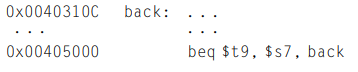
What is the range of instruction addresses to which conditional branches, such as beq and bne, can branch in MIPS? Give your answer in number of instructions relative to the conditional branch instruction.
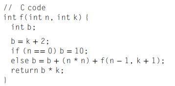
Consider the following high-level function.? (a) Translate the high-level function f into MIPS assembly language. Pay particular attention to properly saving and restoring registers across function calls and using the MIPS preserved register conventions. Clearly comment your code. You can use the
Consider the following C code snippet.? (a) Implement the C code snippet in MIPS assembly language. Use $s0 to hold the variable i. Be sure to handle the stack pointer appropriately. The array is stored on the stack of the setArray function.(b) Assume setArray is the first function called. Draw
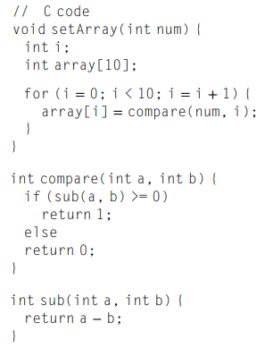
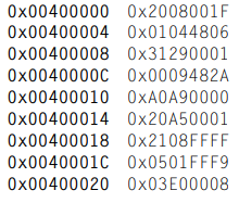
Consider the following MIPS assembly language snippet. The numbers to the left of each instruction indicate the instruction address.? (a) Translate the instruction sequence into machine code. Write the machine code instructions in hexadecimal.(b) List the addressing mode used at each line of
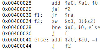
Convert the following beq, j, and jal assembly instructions into machine code. Instruction addresses are given to the left of each instruction.? (a) (b) (c) (d) (e) 0x00401000 beq $t0, $s1, Loop 0x00401004 Ox00401008 Ox0040100C Loop:
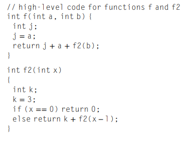
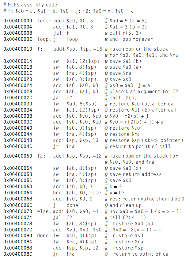
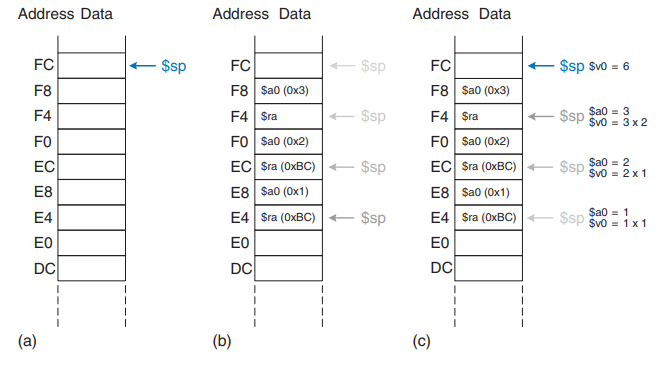
Ben Bitdiddle is trying to compute the function f(a, b) = 2a + 3b for nonnegative b. He goes overboard in the use of function calls and recursion and produces the following high-level code for functions f and f2.? Ben then translates the two functions into assembly language as follows. He also
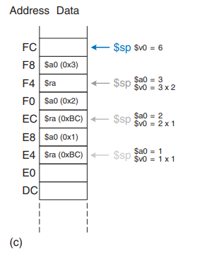
Consider C Code Example 6.27. For this exercise, assume factorial is called with input argument n = 5.(a) What value is in $v0 when factorial returns to the calling function?(b) Suppose you delete the instructions at addresses 0x98 and 0xBC that save and restore $ra. Will the program(1) enter an
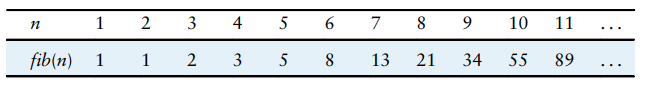
Each number in the Fibonacci series is the sum of the previous two numbers. Table 6.16 lists the first few numbers in the series, fib(n).? (a) What is fib(n) for n = 0 and n = ?1?(b) Write a function called fib in a high-level language that returns the Fibonacci number for any nonnegative value
Convert the high-level function from Exercise 6.18 into MIPS assembly code. Data from Problem 18Write a function in a high-level language for int find42(int array[], int size). size specifies the number of elements in array, and array specifies the base address of the array. The function
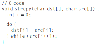
The high-level function strcpy copies the character string src to the character string dst? (a) Implement the strcpy function in MIPS assembly code. Use $s0 for i.(b) Draw a picture of the stack before, during, and after the strcpy function call. Assume $sp = 0x7FFFFF00 just before strcpy is
Write a function in a high-level language for int find42(int array[], int size). size specifies the number of elements in array, and array specifies the base address of the array. The function should return the index number of the first array entry that holds the value 42. If no array entry is 42,
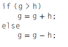
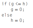
Implement the following high-level code segments using the slt instruction. Assume the integer variables g and h are in registers $s0 and $s1, respectively.? (a)? (b) (c) if (g > h) g = g + h; else g = g – h;
The nori instruction is not part of the MIPS instruction set, because the same functionality can be implemented using existing instructions. Write a short assembly code snippet that has the following functionality: $t0 = $t1 NOR 0xF234. Use as few instructions as possible.
Repeat Exercise 6.14 for the following machine code. $a0 and $a1 are the inputs. $a0 contains a 32-bit number and $a1 is the address of a 32-element array of characters (char).? Data from problem 14 Convert the following program from machine language into MIPS assembly language. The numbers on
Convert the following program from machine language into MIPS assembly language. The numbers on the left are the instruction addresses in memory, and the numbers on the right give the instruction at that address. Then reverse engineer a high-level program that would compile into this assembly
Repeat Exercise 6.12 for the instructions in Exercise 6.11.
Consider I-type instructions.(a) Which instructions from Exercise 6.10 are I-type instructions?(b) Sign-extend the 16-bit immediate of each instruction from part (a) so that it becomes a 32-bit number.? Data From problem 10 Convert the following MIPS assembly code into machine language. Write the
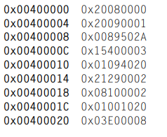
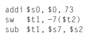
Repeat Exercise 6.10 for the following MIPS assembly code:? Data From problem 10 Convert the following MIPS assembly code into machine language. Write the instructions in hexadecimal.? addi $s0, $0, 73 $t1, -7($t2) sub $t1, $s 7, $s2 SW
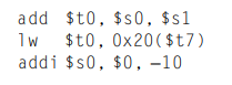
Convert the following MIPS assembly code into machine language. Write the instructions in hexadecimal.? add $t0, $s0, $s1 1w $t0, 0x20( $t7) addi $s0, $0, -10
Repeat Exercise 6.8 for the strings in Exercise 6.7
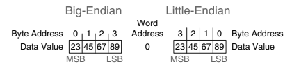
Show how the strings in Exercise 6.6 are stored in a byte-addressable memory on(a) a big-endian machine ?(b) a little-endian machine starting at memory address 0x1000100C. Use a memory diagram similar to Figure 6.4. Clearly indicate the memory address of each byte on each machine. Data From
Repeat Exercise 6.6 for the following strings.(a) howdy (b) lions(c) To the rescue! Data From problem 6Write the following strings using ASCII encoding. Write your final answers in hexadecimal. (a) SOS(b) Cool!(c) (your own name)
Write the following strings using ASCII encoding. Write your final answers in hexadecimal. (a) SOS(b) Cool!(c) (your own name)
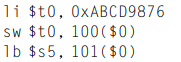
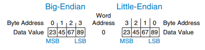
Explain how the following program can be used to determine whether a computer is big-endian or little-endian:? li $t0, 0XABCD9876 Sw $t0, 100( $0) lb $s5, 101($0)
Repeat Exercise 6.3 for memory storage of a 32-bit word stored at memory word 15 in a byte-addressable memory.? Data from problem 3 Consider memory storage of a 32-bit word stored at memory word 42 in a byte-addressable memory.(a) What is the byte address of memory word 42?(b) What are the byte
Consider memory storage of a 32-bit word stored at memory word 42 in a byte-addressable memory.(a) What is the byte address of memory word 42?(b) What are the byte addresses that memory word 42 spans?(c) Draw the number 0xFF223344 stored at word 42 in both big-endian and little-endian machines.
The MIPS architecture has a register set that consists of 32-bit registers. Is it possible to design a computer architecture without a register set? If so, briefly describe the architecture, including the instruction set. What are advantages and disadvantages of this architecture over the MIPS
Give three examples from the MIPS architecture of each of the architecture design principles:(1) simplicity favors regularity(2) make the common case fast(3) smaller is faster(4) good design demands good compromises. Explain how each of your examples exhibits the design principle.
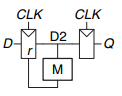
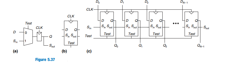
Write the HDL for a 4-bit scannable flip-flop like the one shown in Figure 5.37. Simulate and test your HDL module to prove that it functions correctly. Do D, D2 DN-1 CLK- CLK D 아- D Q 아 Test ... S, Sout S. Sout Sn Sout S, Sout CLK in in 아- mos S. out Test Test Test Test Test Sin 1 Test Sout
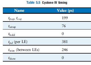
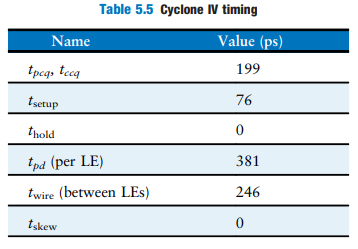
You would like to use an FPGA to implement an M&M sorter with a color sensor and motors to put red candy in one jar and green candy in another. The design is to be implemented as an FSM using a Cyclone IV FPGA. According to the data sheet, the FPGA has timing characteristics shown in Table 5.5.
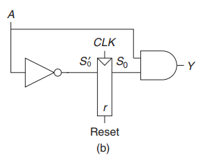
Repeat Exercise 5.57 for the FSM of Figure 3.31(b).? A CLK Só So Y Reset (b)
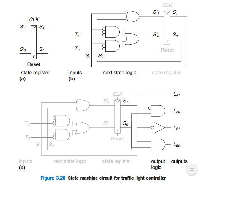
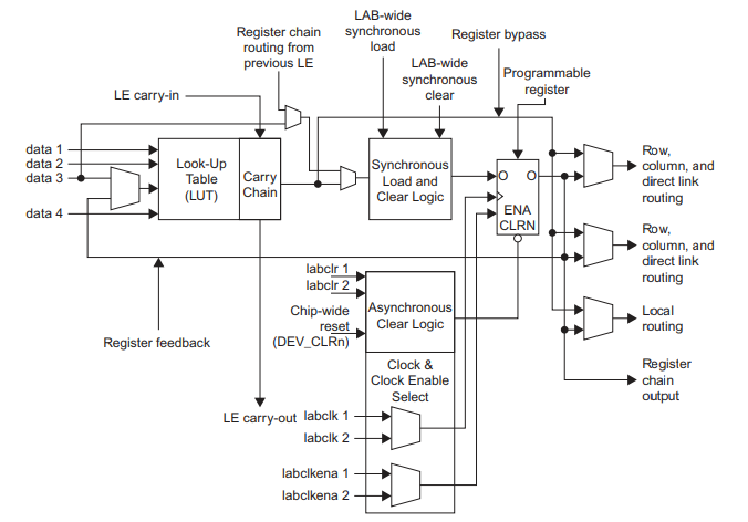
Consider the Cyclone IV LE shown in Figure 5.58. According to the datasheet, it has the timing specifications given in Table 5.5.(a) What is the minimum number of Cyclone IV LEs required to implement the FSM of Figure 3.26?(b) Without clock skew, what is the fastest clock frequency at which this
Repeat Exercise 5.55 for the following functions.(a) an eight-input priority encoder(b) a 3:8 decoder(c) a 4-bit carry propagate adder (with no carry in or out)(d) the FSM from Exercise 3.22(e) the Gray code counter from Exercise 3.27
How many Cyclone IV FPGA LEs are required to perform each of the following functions? Show how to configure one or more LEs to perform the function. You should be able to do this by inspection, without performing logic synthesis.(a) the combinational function from Exercise 2.13(c)(b) the
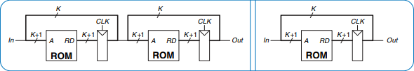
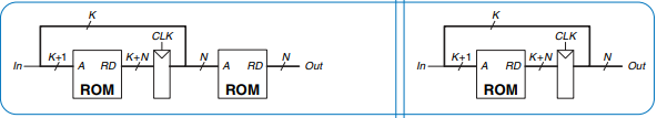
Consider the ROM circuits in Figure 5.65. For each row, can the circuit in column I be replaced by an equivalent circuit in column II by proper programming of the latter?s ROM?? (a) (b) (c) (d) N N RDH A RDH N RD ROM ROM ROM
Specify the size of a ROM that you could use to program each of the following combinational circuits. Is using a ROM to implement these functions a good design choice? Explain why or why not.(a) a 16-bit adder/subtractor with Cin and Cout (b) an 8 × 8 multiplier(c) a 16-bit priority encoder
2 Implement the functions from Exercise 5.51 using a 4 × 8 × 3 PLA. You may use dot notation.
Implement the following functions using a single 16 × 3 ROM. Use dot notation to indicate the ROM contents. (a) X = AB +BC̅D + A̅B̅ (b) Y = AB +BD (c) Z = A +B+ C + D
The extraterrestrial life project team has just discovered aliens living on the bottom of Mono Lake. They need to construct a circuit to classify the aliens by potential planet of origin based on measured features available from the NASA probe: greenness, brownness, sliminess, and ugliness. Careful
Flash EEPROM, simply called Flash memory, is a fairly recent invention that has revolutionized consumer electronics. Research and explain how Flash memory works. Use a diagram illustrating the floating gate. Describe how a bit in the memory is programmed. Properly cite your sources.
The English language has a good deal of redundancy that allows us to reconstruct garbled transmissions. Binary data can also be transmitted in redundant form to allow error correction. For example, the number 0 could be coded as 00000 and the number 1 could be coded as 11111. The value could then
An N-bit Johnson counter consists of an N-bit shift register with a reset signal. The output of the shift register (Sout) is inverted and fed back to the input (Sin). When the counter is reset, all of the bits are cleared to 0.(a) Show the sequence of outputs, Q3:0, produced by a 4-bit Johnson
Modify the counter from Exercise 5.44 such that the counter will either increment by 4 or load a new 32-bit value, D, on each clock edge, depending on a control signal Load. When Load = 1, the counter loads the new value D.
Design a 32-bit counter that adds 4 at each clock edge. The counter has reset and clock inputs. Upon reset, the counter output is all 0.
Build a 32-bit synchronous Up/Down counter. The inputs are Reset and Up. When Reset is 1, the outputs are all 0. Otherwise, when Up = 1, the circuit counts up, and when Up = 0, the circuit counts down.
When adding two floating-point numbers, the number with the smaller exponent is shifted. Why is this? Explain in words and give an example to justify your explanation.
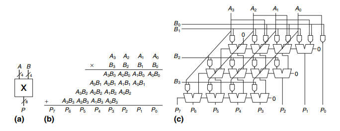
Find the critical path for the 4 ? 4 divider from Figure 5.20 in terms of a 2:1 mux delay (tMUX), an adder delay (tFA), and an inverter delay (tINV). What is the delay of an N ? N divider built in the same way? A3 A2 A, Ao Bo B, A3 A2 B, B2 Bị B. A, Ao B2 A B to te AB, AB, A,B, ABo AB, AB, A,B,
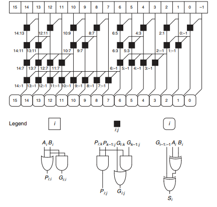
Design the 16-bit prefix adder of Figure 5.7 in an HDL. Simulate and test your module to prove that it functions correctly.? 13 12 11 10 9 e -1 7 65 4 3 2 15 14 10:9 8:7 6:5 4:3 2:1 0:-1 14:13 12:11 14:11 13:11 10:7T9:7 6:3 5:3 2:-1 1:-1 14:7 13:7 12:711:7 6:-1 5:-1 4:-1 3:-1 14:1 13-1 12-1 J11-1
What is the delay for the following types of 64-bit adders? Assume that each two-input gate delay is 150 ps and that a full adder delay is 450 ps.(a) a ripple-carry adder(b) a carry-lookahead adder with 4-bit blocks(c) a prefix adder
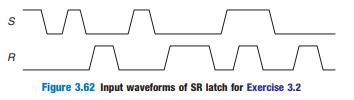
Write an HDL module for the serial two?s complementer from Question 3.2.? Data from problem 3.2 Given the input waveforms shown in Figure 3.62, sketch the output, Q, of an SR latch.? Figure 3.62 Input waveforms of SR latch for Exercise 3.2
Write an HDL module for the FSM from Exercise 3.30. Data from problem 3.30Design an FSM with one input, A, and two outputs, X and Y. X should be 1 if A has been 1 for at least three cycles altogether (not necessarily consecutively). Y should be 1 if A has been 1 for at least two consecutive
Write an HDL module for the FSM from Exercise 3.29.? Data from problem 3.29 Your company, Detect-o-rama, would like to design an FSM that takes two inputs, A and B, and generates one output, Z. The output in cycle n, Zn, is either the Boolean AND or OR of the corresponding input An and the
Write an HDL module for the UP/DOWN Gray code counter from Exercise 3.28. Data from problem 3.28Extend your modulo 8 Gray code counter from Exercise 3.27 to be an UP/DOWN counter by adding an UP input. If UP = 1, the counter advances to the next number. If UP = 0, the counter retreats to the
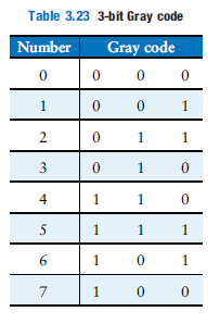
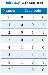
Write an HDL module for the Gray code counter from Exercise 3.27.? Data from problem 3.27 Gray codes have a useful property in that consecutive numbers differ in only a single bit position. Table 3.23 lists a 3-bit Gray code representing the numbers 0 to 7. Design a 3-bit modulo 8 Gray code
Write an HDL module for the soda machine dispenser from Exercise 3.26. Data from problem 3.26You have been enlisted to design a soda machine dispenser for your department lounge. Sodas are partially subsidized by the student chapter of the IEEE, so they cost only 25 cents. The machine accepts
Write an HDL module for the daughter snail from Exercise 3.25. Data from problem 3.25Alyssa P. Hacker’s snail has a daughter with a Mealy machine FSM brain. The daughter snail smiles whenever she slides over the pattern 1101 or the pattern 1110. Sketch the state transition diagram for this
Write an HDL module for the improved traffic light controller from Exercise 3.24. Data from problem 3.24Accidents are still occurring at the intersection of Academic Avenue and Bravado Boulevard. The football team is rushing into the intersection the moment light B turns green. They are
Write an HDL module for the FSM with the state transition diagram given in Figure 3.70 from Exercise 3.23.
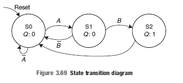
Write an HDL module for the FSM with the state transition diagram given in Figure 3.69 from Exercise 3.22.? Data from Problem 3.22 Describe in words what the state machine in Figure 3.69 does. Using binary state encodings, complete a state transition table and output table for the ?FSM. Write
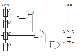
Write an HDL module describing the circuit in Figure 3.42.? Data From chapter 3 CLK CLK A n1 B the X'
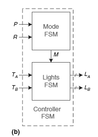
Write three HDL modules for the factored parade mode traffic light controller from Example 3.8. The modules should be called controller, mode, and lights, and they should have the inputs and outputs shown in Figure 3.33(b).? Data From Problem Chapter 2 P Mode FSM M TA Lights FSM Le Controller
Write an HDL module for the traffic light controller from Section 3.4.1.
Write an HDL module for the latch from Figure 3.18. Use one assignment statement for each gate. Specify delays of 1 unit or 1 ns to each gate. Simulate the latch and show that it operates correctly. Then increase the inverter delay. How long does the delay have to be before a race condition causes
Write an HDL module for a JK flip-flop. The flip-flop has inputs, clk, J, and K, and output Q. On the rising edge of the clock, Q keeps its old value if J = K = 0. It sets Q to 1 if J = 1, resets Q to 0 if K = 1, and inverts Q if J=K=1.
Write an HDL module for an SR latch.
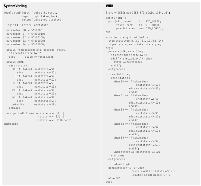
Sketch the state transition diagram for the FSM described by the following HDL code. An FSM of this nature is used in a branch predictor on some microprocessors.? SystemVerilog VHDL library IEEE; use IEEE.STD LOGIC_1164. all: module fsm1(input logic clk, reset. input logic taken, back, output
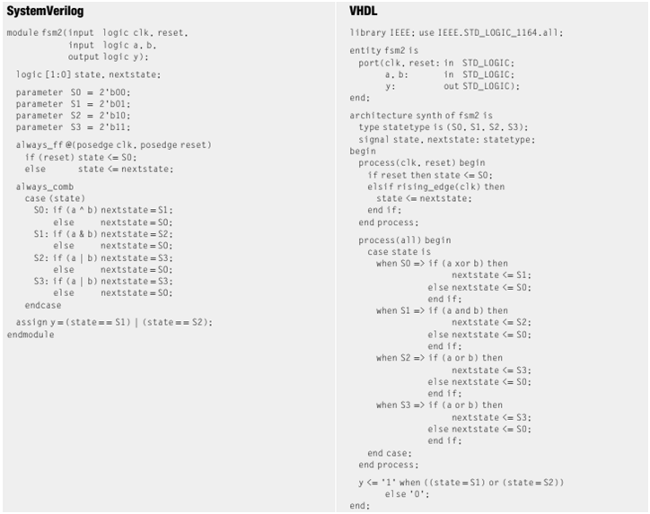
Sketch the state transition diagram for the FSM described by the following HDL code.? SystemVerilog VHDL module fsm2(input logic clk. reset. 11brary IEEE; use IEEE.STD_LOGIC_1164.all: input logic a. b. output logic y): logic [1:0] state, nextstate: entity fsm2 is port(clk, reset: in STD_LOGIC: in
Write an HDL module that implements the binary-to-thermometer code converter from Exercise 2.38. Data from problem 2.38An M-bit thermometer code for the number k consists of k 1’s in the least significant bit positions and M – k 0’s in all the more significant bit positions. A
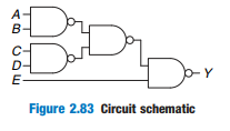
Write an HDL module that implements the circuit from Exercise 2.26.? Data from Problem 2. 26 Using De Morgan equivalent gates and bubble pushing methods, redraw the circuit in Figure 2.83 so that you can find the Boolean equation by inspection. Write the Boolean equation. ? A D- E- Figure 2.83
Write HDL modules that implement the Boolean equations from Exercise 2.13.Data from Problem 14Write an HDL module for a 2:4 decoder
Write an HDL module for a 2:4 decoder.
A synchronizer is built from a pair of flip-flops with tsetup = 50 ps, T0 = 20 ps, and τ = 30 ps. It samples an asynchronous input that changes 108 times per second. What is the minimum clock period of the synchronizer to achieve a mean time between failures (MTBF) of 100 years?
Extend your modulo 8 Gray code counter from Exercise 3.27 to be an UP/DOWN counter by adding an UP input. If UP = 1, the counter advances to the next number. If UP = 0, the counter retreats to the previous number.? Data From Problem 27 Gray codes have a useful property in that consecutive numbers
Why must N be odd in Exercise 3.16? Data From Problem 16Suppose a ring oscillator is built from N inverters connected in a loop. Each inverter has a minimum delay of tcd and a maximum delay of tpd. If N is odd, determine the range of frequencies at which the oscillator might operate.
Sketch a reasonably simple combinational circuit implementing each of the functions from Exercise 2.5. Reasonably simple means that you are not wasteful of gates, but you don’t waste vast amounts of time checking every possible implementation of the circuit either.
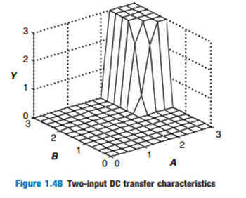
While walking down a dark alley, Ben Bit diddle encounters a two input gate with the transfer function shown in Figure 1.48. The inputs are A and B and the output is Y. A Figure 1.48 Two-Input DC transfer characteristics
Write an HDL module that implements the modified priority encoder from Exercise 2.37. Data from problem 2.37Design a modified priority encoder that receives an 8-bit input, A7:0, and produces two 3-bit outputs, Y2:0 and Z2:0 Y indicates the most significant bit of the input that is TRUE.
Write an HDL module that implements the priority encoder from Exercise 2.36. Data from Problem 2.36A priority encoder has 2N inputs. It produces an N-bit binary output indicating the most significant bit of the input that is TRUE, or 0 if none of the inputs are TRUE. It also produces an output
Write an HDL module that implements the functions from Exercise 2.35. Data from Problem 2.35A circuit has four inputs and two outputs. The inputs Α3:0 represent a number from 0 to 15. Output P should be TRUE if the number is prime (0 and 1 are not prime, but 2, 3, 5, and so on, are prime).
Write an HDL module that implements the logic function from Exercise 2.28. Pay careful attention to how you handle don’t cares. Data from Problem 2.28Find a minimal Boolean equation for the function in Figure 2.85. Remember to take advantage of the don’t care entries. A B х х х х
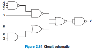
Write an HDL module that implements the circuit from Exercise 2.27. Data From Problem 2.27Repeat Exercise 2.26 for the circuit in Figure 2.84. D-Y Figure 2.84 Circuit schematic
Write an HDL module for a 6:64 decoder using three instances of the 2:4 decoders from Exercise 4.13 and a bunch of three-input AND gates. Data from problem 13Write an HDL module for a 2:4 decoder.
Write an HDL module for an eight-input priority circuit.
Section 4.5.4 pointed out that a synchronizer could be correctly described with blocking assignments if the assignments were given in the proper order. Think of a simple sequential circuit that cannot be correctly described with blocking assignments, regardless of order.
Repeat Exercise 4.9 using a 4:1 multiplexer and as many NOT gates as you need.
Write a structural module to compute the logic function, y = ab̅ + b̅c̅+a̅bc, using multiplexer logic. Use the 8:1 multiplexer from Exercise 4.8.Data From Problem 8Write an 8:1 multiplexer module called mux8 with inputs s2:0, d0, d1, d2, d3, d4, d5, d6, d7, and output y.
Write an 8:1 multiplexer module called mux8 with inputs s2:0, d0, d1, d2, d3, d4, d5, d6, d7, and output y.
Write a self-checking testbench for Exercise 4.6. Create a test vector file containing all 16 test cases. Simulate the circuit and show that it works. Introduce an error in the test vector file and show that the testbench reports a mismatch.
Write an HDL module for a hexadecimal seven-segment display decoder. The decoder should handle the digits A, B, C, D, E, and F as well as 0–9.
Write an HDL module called minority. It receives three inputs, a, b, and c. It produces one output, y, that is TRUE if at least two of the inputs are FALSE.
Write a self-checking testbench for Exercise 4.3. Create a test vector file containing all 16 test cases. Simulate the circuit and show that it works. Introduce an error in the test vector file and show that the testbench reports a mismatch.
Write an HDL module that computes a four-input XOR function. The input is a3:0, and the output is y.
What does the following SystemVerilog statement do? result = | (data[15:0] & 16'hC820);
Sketch a schematic of the circuit described by the following HDL code. Simplify the schematic so that it shows a minimum number of gates. SystemVerilog VHDL module exercise2(input logic [3:0] a. output logic (1:0] y): library IEEE; use IEEE.STD_LOGIC_1164.all; entity exercise2 is port(a: in
Explain the difference between blocking and non blocking assignments in SystemVerilog. Give examples.
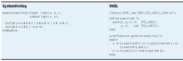
Sketch a schematic of the circuit described by the following HDL code. Simplify the schematic so that it shows a minimum number of gates. SystemVerilog VHDL module exerctsel (input 1ogt ca, b. c. output l ogi c y. z); 1ibrary IEEE; use IEEE.STD LOGIC_1164.all: assign y = a & b &c|a &b & -c | a & -b
Write a line of HDL code that gates a 32-bit bus called data with another signal called sel to produce a 32-bit result. If sel is TRUE, result = data. Otherwise, result should be all 0’s.
Ben Bitdiddle invents a new and improved synchronizer in Figure 3.76 that he claims eliminates metastability in a single cycle. He explains that the circuit in box M is an analog “metastability detector” that produces a HIGH output if the input voltage is in the forbidden zone between VIL and
You have built a synchronizer using flip-flops with T0 = 20 ps and τ = 30 ps. Your boss tells you that you need to increase the MTBF by a factor of 10. By how much do you need to increase the clock period?
Showing 100 - 200
of 430
1
2
3
4
5
Step by Step Answers


![SystemVerilog VHDL module exercise2(input logic [3:0] a. output logic (1:0] y): library IEEE; use IEEE.STD_LOGIC_1164.al](https://dsd5zvtm8ll6.cloudfront.net/si.question.images/images/question_images/1547/3/0/6/9565c3a07cce671d1547289597013.jpg)