New Semester
Started
Get
50% OFF
Study Help!
--h --m --s
Claim Now
Question Answers
Textbooks
Find textbooks, questions and answers
Oops, something went wrong!
Change your search query and then try again
S
Books
FREE
Study Help
Expert Questions
Accounting
General Management
Mathematics
Finance
Organizational Behaviour
Law
Physics
Operating System
Management Leadership
Sociology
Programming
Marketing
Database
Computer Network
Economics
Textbooks Solutions
Accounting
Managerial Accounting
Management Leadership
Cost Accounting
Statistics
Business Law
Corporate Finance
Finance
Economics
Auditing
Tutors
Online Tutors
Find a Tutor
Hire a Tutor
Become a Tutor
AI Tutor
AI Study Planner
NEW
Sell Books
Search
Search
Sign In
Register
study help
business
organization development
Computer Organization 5th Edition V Carl Hamacher, Carl Hamacher, Zvonko G Vranesic, Safwat G Zaky - Solutions
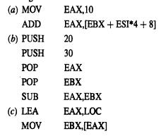
Assume the following register and memory contents in an IA-32 computer: Register EBX contains 1000. Register ESI contains 2. The numbers 1, 2, 3, 4, 5, and 6, are stored in successive doubleword locations starting at memory address 1000. The address label LOC represents address 1008. What is the
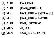
Which of the following IA-32 instructions would cause the assembler to issue a syntax error message? Why? (a) ADD EAX,EAX (b) ADD [EAX],[EBX+4] (c) SUB EAX,[EBX + ESI*4 +20] (d) SUB EAX,[EBX + ESI*10] (e) ADD EAX,-31728542 (f) MOV 20,EAX (g) MOV EAX,[EBP + ESP*4]
A program trace is a listing of the contents of certain registers and memory locations at different times during the execution of a program. List the contents of registers EAX, EBX, and ECX after each of the first three executions of the LOOP instruction in the program in Figure 3.40b. Present the
Write an IA-32 program that compares the corresponding bytes of two lists of bytes and places the larger byte in a third list. The two lists start at byte locations X and Y, and the larger-byte list starts at LARGER. The length of the lists is stored in memory location N.
An IA-32 program is required for the following character manipulation task: A string of n characters is stored in the memory in consecutive byte locations, beginning at location STRING. Another, shorter string of m characters is stored in consecutive byte locations, beginning at location SUBSTRING.
Write an IA-32 program that generates the first n numbers of the Fibonacci series. In this series, the first two numbers are 0 and 1, and each subsequent number is generated by adding the preceding two numbers. For example, for n = 8, the series is 0, 1, 1, 2, 3, 5, 8, 13 Your program should store
Write an IA-32 program to convert a word of text from lowercase to uppercase. The word consists of ASCII characters stored in successive byte locations in the memory, starting at location WORD and ending with a space character. (See Appendix E for the ASCII code.)
The list of student marks shown in Figure 2.14 is changed to contain j test scores for each student. Assume that there are n students. Write an IA-32 program for computing the sums of the scores on each test and store these sums in the memory doubleword locations at addresses SUM, SUM+4, SUM+8,....
Write an IA-32 program to reverse the order of bits in register EAX. For example, if the starting pattern in EAX is 1110... 0100, the result left in EAX should be 00100111. (Hint: Use shift and rotate operations.)LO1
Consider the queue structure described in Problem 2.18. Write IA-32 APPEND and REMOVE routines that transfer data between a processor register and the queue. Be careful to inspect and update the state of the queue and the pointers each time an operation is attempted and performed.
Write an IA-32 program that reads n characters from a keyboard and echoes them back to a display after pushing them onto a user stack as they are read. Use register EBX as the stack pointer. The count value n is stored in memory doubleword location N.
Assume that the average time taken to fetch and execute an instruction in the program in Figure 3.44 is 10 nanoseconds. If keyboard characters are entered at the rate of 10 per second, approximately how many times is the JNC READ instruction executed per character entered? Assume that the time
In the IA-32 program in Figure 3.44, "in-line" code is used to read a line of charac- ters and display them. Rewrite this program in the form of a main program that calls a subroutine named GETCHAR to read a single character and calls another subrou- tine named PUTCHAR to display a single
Repeat problem 3.63, passing parameters on the processor stack.LO1
Write an IA-32 program to accept three decimal digits from a keyboard. Each digit is represented in the ASCII code (see Appendix E). Assume that these three digits represent a decimal integer in the range 0 to 999 and convert the integer into a binary number representation. The high-order digit is
The decimal-to-binary conversion program of Problem 3.65 is to be implemented us- ing two nested subroutines. The main program that calls the first subroutine passes two parameters by pushing them onto the processor stack. The first parameter is the address of a 3-byte memory buffer area for
Consider an array of numbers A(i,j), where i = 0 through n-1 is the row index and j = 0 through m-1 is the column index. The array is stored in the memory of a IA-32 computer one row after another, with elements of each row occupying m successive doubleword locations. Write an IA-32 subroutine for
Using the format for presenting results that is described in Problem 3.53, give a program trace for the byte-sorting program in Figure 3.50b. Show the contents of registers EDI, ECX, and DL, and list byte locations LIST, LIST+1,..., LIST + 4 for a 5-byte list after each execution of the last
Rewrite the byte-sorting program in Figure 3.50b as a subroutine that sorts a list of 32-bit positive integers. The calling program should pass the list address to the sub- routine. The first 32-bit quantity at that location is the number of entries in the list, followed by the numbers to be sorted.
Consider the byte-sorting program of Figure 3.50b. During each pass through a sublist, LIST(j) through LIST(0), list entries are swapped whenever LIST(k) > LIST(j). An alternative strategy is to keep track of the address of the largest value in the sublist, and to perform, at most, one swap at the
Assume that the list of student test scores shown in Figure 2.14 is stored in the memory as a linked list as shown in Figure 2.36. Write an IA-32 program that accomplishes the same thing as the program in Figure 2.15. The head record is stored at memory location 1000.LO1
The linked-list insertion subroutine in Figure 3.51 does not check if the ID of the new record matches that of a record already in the list. What happens in the execution of the subroutine if this is the case? Modify the subroutine to return the address of the matching record in register EDX if
The linked-list deletion subroutine in Figure 3.52 assumes that a record with the ID contained in register RIDNUM is in the list. What happens in the execution of the subroutine if there is no record with this ID? Modify the subroutine to return a zero in RIDNUM if deletion is successful, or leave
The input status bit in an interface circuit is cleared as soon as the input data buffer is read. Why is this important?LO1
Write a program that displays the contents of 10 bytes of the main memory in hexadec- imal format on a video display. Use either the assembler instructions of a processor of your choice or pseudo-instructions. Start at location LOC in the memory, and use two hex characters per byte. The contents of
The address bus of a computer has 16 address lines, A15-0. If the address assigned to one device is 7CA416 and the address decoder for that device ignores lines Ag and A9, what are all the addresses to which this device will respond?
What is the difference between a subroutine and an interrupt-service routine?
The discussion in this chapter assumed that interrupts are not acknowledged until the current machine instruction completes execution. Consider the possibility of suspend- ing operation of the processor in the middle of executing an instruction in order to acknowledge an interrupt. Discuss the
Three devices, A, B, and C, are connected to the bus of a computer. I/O transfers for all three devices use interrupt control. Interrupt nesting for devices A and B is not allowed, but interrupt requests from C may be accepted while either A or B is being serviced. Suggest different ways in which
Consider a computer in which several devices are connected to a common interrupt- request line, as in Figure 4.8a. Explain how you would arrange for interrupts from device j to be accepted before the execution of the interrupt-service routine for device i is completed. Comment in particular on the
Consider the daisy chain arrangement in Figure 4.8a. Assume that after a device gen- erates an interrupt request, it turns off that request as soon as it receives the interrupt- acknowledge signal. Is it still necessary to disable interrupts in the processor before entering the interrupt-service
Successive data blocks of N bytes each are to be read from a character-oriented input device, and program PROG is to perform some computation on each block of data. Write a control program, CONTROL, for the 68000, ARM, or Pentium processors that will perform the following functions. (a) Read data
A computer is required to accept characters from 20 video terminals. The main memory area to be used for storing data for each terminal is pointed to by a pointer PNTR, where n = 1 through 20. Input data must be collected from the terminals while another program PROG is being executed. This may be
Consider an I/O device that uses the vectored-interrupt capability of the 68000 processor. (a) Describe the sequence of steps that take place when the processor receives an interrupt request, and give the number of bus transfers required during each of these steps. Do not give details of bus
A logic circuit is needed to implement the priority network shown in Figure 4.86. The network handles three interrupt request lines. When a request is received on line INTRI, the network generates an acknowledgment on line INTAI. If more than one request is received, only the highest-priority
Interrupts and bus arbitration require means for selecting one of several requests based on their priority. Design a circuit that implements a rotating-priority scheme for four input lines, REQ1 through REQ4. Initially, REQ1 has the highest and REQ4 the lowest priority. After some line receives
The 68000 processor has a set of three lines called IPL2-0 that are used to signal interrupt requests. The 3-bit binary number on these lines is interpreted by the processor as representing the highest-priority device requesting an interrupt. Design a priority encoder circuit that accepts interrupt
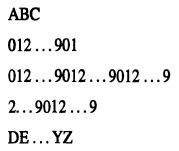
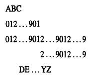
(This problem is suitable for use as a laboratory experiment.) Given a video terminal connected to the computer in your laboratory, complete the following two assignments.(a) Write an I/O routine A that prints letters in alphabetical order. It prints two lines as follows, and then stops: ABC...YZ
(This problem is suitable for use as a laboratory experiment.) In Problem 4.15, when the printing of a sequence is interrupted and later resumed, the sequence continues at the beginning of a new line. It is desired to add cursor movement control functions such that when printing of a sequence is
Consider the breakpoint scheme described in Section 4.2.5. A software-interrupt in- struction replaces a program instruction where the breakpoint is inserted. Before it returns to the original program. the debugging software puts the original program instruction back in its place, thus removing the
The software interrupt instruction, SWI, of the ARM can be used by a program to call the operating system to request some service. The service being requested is specified in the low-order 8 bits of the instruction. Each of the services provided by the operating system is performed by a separate
The interrupt-request line, which uses the open-collector scheme, carries a signal that is the logical OR of the requests from all the devices connected to it. In a different application, it is required to generate a signal that indicates that all devices connected to the bus are ready. Explain how
In some computers, the processor responds only to the leading edge of the interrupt- request signal on one of its interrupt-request lines. What happens if two independent devices are connected to this line?
In the arrangement in Figure 4.20, a device becomes the bus master only when it receives a low-to-high transition on its bus grant input. Assume that device 1 requests the bus and receives a grant. While it is still using the bus, device 3 asserts its BR output. Draw a timing diagram showing how
Assume that in the bus arbitration arrangement in Figure 4.20, the processor keeps asserting BG1 as long as BR is asserted. When device i is requesting the bus, it becomes the bus master only when it receives a low-to-high transition on its BGi input. (a) Assume that devices are allowed to assert
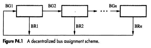
Consider the daisy-chain arrangement shown in Figure P4.1, in which the bus-request signal is fed back directly as the bus grant. Assume that device 3 requests the bus andbegins using it. When device 3 is finished, it deactivates BR3. Assume that the delay from BGi to BG(i + 1) in any device isd.
Shortly after device 3 in Problem 4.23 releases the bus, devices 1 and 5 request the bus simultaneously. Show that they can both receive a bus grant.LO1
Consider the bus arbitration scheme shown in Figure 4.20. Assume that a local signal called BUSREQ in the device interface circuit is equal to 1 whenever the device needs to use the bus. Design the part of the interface circuit that has BUSREQ, BGI, and BBSY as inputs and that generates BR, BG(i +
Consider the arbitration circuit shown in Figure 4.22. Assume that the priority code for a device is stored in a register in the interface circuit. Design a circuit to implement this ar- bitration scheme. Arbitration begins when Start-Arbitration is asserted. A little later, the arbitration circuit
How would the timing diagram in Figure 4.26 be affected if the distance between the processor and the I/O device is increased? How can this increased distance be accom- modated in the case of Figure 4.24?LO1
An industrial plant uses several limit sensors for monitoring temperature, pressure, and other factors. The output of each sensor consists of an ON/OFF switch, and eight such sensors need to be connected to the bus of a small computer. Design an appropriate interface so that the state of all eight
Design an appropriate interface for connecting a seven-segment display as an output device on a synchronous bus. (See Figure A.37 in Appendix A for a description of a seven-segment display.)LO1
Add an interrupt capability to the interface in Figure 4.29. Show how you can introduce an interrupt enable bit, which can be set or cleared by the processor as bit 6 of the status register of the interface. The interface should assert an interrupt request line, INTR, when interrupts are enabled
The bus of a processor uses the multiple-cycle scheme described in Section 4.5.1. The speed of a memory unit is such that a read operation follows the timing diagram shown in Figure 4.25. Design an interface circuit to connect this memory unit to the bus.LO1
Consider a write operation on a bus that uses the multiple-cycle scheme described in Section 4.5.1. Assume that the processor can send both address and data in the first clock cycle of a bus transaction. But the memory requires two clock cycles after that to store the data. (a) Can the bus be used
Figures 4.24 to 4.26 provide three different approaches to bus design. What happens in each case if the addressed device does not respond due to a malfunction? What problems would this cause and what remedies are possible?LO1
In the timing diagram in Figure 4.25, the processor maintains the address on the bus until it receives a response from the device. Is this necessary? What additions are needed on the device side if the processor sends an address for one cycle only?LO1
Consider a synchronous bus that operates according to the timing diagram in Fig- ure 4.24. The address transmitted by the processor appears on the bus after 4 ns. The propagation delay on the bus wires between the processor and different devices con- nected varies from 1 to 5 ns, address decoding
The time required for a complete bus transfer in the case of Figure 4.26 varies depending on the delays involved. Consider a bus having the same parameters as in Problem 4.35. What is the minimum and maximum bus cycle time?LO1
Give a block diagram similar to the one in Figure 5.10 for a 8M 32 memory using 512K x 8 memory chips.LO1
Consider the dynamic memory cell of Figure 5.6. Assume that C = 50 femtofarads (10-15 F) and that leakage current through the transistor is about 9 picoamperes (10-12 A). The voltage across the capacitor when it is fully charged is equal to 4.5 V. The cell must be refreshed before this voltage
In the bottom right corner of Figure 5.8 there are data input and data output registers. Draw a circuit that can implement one bit of each of these registers, and show the required connections to the block "Read/Write circuits & latches" on one side and the data bus on the other side.LO1
Consider a main memory constructed with SDRAM chips that have timing requirements depicted in Figure 5.9, except that the burst length is 8. Assume that 32 bits of data are transferred in parallel. If a 133-MHz clock is used, how much time does it take to transfer: (a) 32 bytes of data (b) 64 bytes
Criticize the following statement: "Using a faster processor chip results in a correspond- ing increase in performance of a computer even if the main memory speed remains the same."LO1
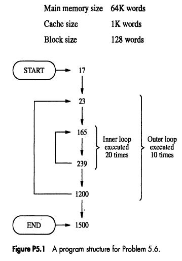
A program consists of two nested loops - a small inner loop and a much larger outer loop. The general structure of the program is given in Figure P5.1. The decimal memory addresses shown delineate the location of the two loops and the beginning and end of the total program. All memory locations in
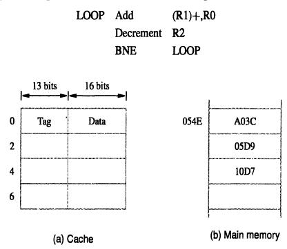
A computer uses a small direct-mapped cache between the main memory and the processor. The cache has four 16-bit words, and each word has an associated 13-bit tag, as shown in Figure P5.2a. When a miss occurs during a read operation, the requested word is read from the main memory and sent to the
Repeat Problem 5.7, assuming only instructions are stored in the cache. Data operands are fetched directly from the main memory and not copied into the cache. Why does this choice lead to faster execution than when both instructions and data are written into the cache?LO1
A block-set-associative cache consists of a total of 64 blocks divided into 4-block sets. The main memory contains 4096 blocks, each consisting of 128 words. (a) How many bits are there in a main memory address? (b) How many bits are there in each of the TAG, SET, and WORD fields?LO1
A computer system has a main memory consisting of 1M 16-bit words. It also has a 4K-word cache organized in the block-set-associative manner, with 4 blocks per set and 64 words per block. (a) Calculate the number of bits in each of the TAG, SET, and WORD fields of the main memory address format.
Repeat Problem 5.10, assuming that whenever a block is to be brought from the main memory and the corresponding set in the cache is full, the new block replaces the most recently used block of this set.LO1
Section 5.5.3 illustrates the effect of different cache-mapping techniques, using the program in Figure 5.19. Suppose that this program is changed so that in the second loop the elements are handled in the same order as in the first loop, that is, the control for the second loop is specified
A byte-addressable computer has a small data cache capable of holding eight 32-bit words. Each cache block consists of one 32-bit word. When a given program is executed, the processor reads data from the following sequence of hex addresses: 200, 204, 208, 20C, 2F4, 2F0, 200, 204, 218, 21C, 24C, 2F4
Repeat Problem 5.13, assuming that each cache block consists of two 32-bit words. For part (c), use a two-way set-associative cache.LO1
How might the value of k in the interleaved memory system of Figure 5.25b influence block size in the design of a cache memory to be used with the system?LO1
In many computers the cache block size is in the range of 32 to 128 bytes. What would be the main advantages and disadvantages of making the size of cache blocks larger or smaller?LO1
Consider the effectiveness of interleaving with respect to the size of cache blocks. Using calculations similar to those in Section 5.6.2, estimate the performance improvement for block sizes of 16, 8, and 4 words. Assume that all words loaded into the cache are accessed by the processor at least
Assume a computer has L1 and L2 caches, as discussed in Section 5.6.3. The cache blocks consist of 8 words. Assume that the hit rate is the same for both caches and that it is equal to 0.95 for instructions and 0.90 for data. Assume also that the times needed to access an 8-word block in these
Repeat Problem 5.18, assuming that a cache block consists of 4 words. Estimate an appropriate value for C2, assuming that the L2 cache is implemented with SRAM chips.LO1
Consider the following analogy for the concept of caching. A serviceman comes to a house to repair the heating system. He carries a toolbox that contains a number of tools that he has used recently in similar jobs. He uses these tools repeatedly, until he reaches a point where other tools are
A 1024 x 1024 array of 32-bit numbers is to be "normalized" as follows. For each column, the largest element is found and all elements of the column are divided by this maximum value. Assume that each page in the virtual memory consists of 4K bytes, and that 1M bytes of the main memory are
Consider a computer system in which the available pages in the physical memory are divided among several application programs. When all the pages allocated to a program are full and a new page is needed, the new page must replace one of the resident pages. The operating system monitors the page
In a computer with a virtual-memory system, the execution of an instruction may be interrupted by a page fault. What state information has to be saved so that this instruction can be resumed later? Note that bringing a new page into the main memory involves a DMA transfer, which requires execution
When a program generates a reference to a page that does not reside in the physical main memory, execution of the program is suspended until the requested page is loaded into the main memory. What difficulties might arise when an instruction in one page has an operand in a different page? What
A disk unit has 24 recording surfaces. It has a total of 14,000 cylinders. There is an average of 400 sectors per track. Each sector contains 512 bytes of data. (a) What is the maximum number of bytes that can be stored in this unit? (b) What is the data transfer rate in bytes per second at a
The seek time plus rotational delay in accessing a particular data block on a disk is usually much longer than the data flow period for most disk transfers. Consider a long sequence of accesses to the 3.5-inch disk given as an example in Section 5.9.1, for either Read or Write operations in which
The average seek time and rotational delay in a disk system are 6 ms and 3 ms, re- spectively. The rate of data transfer to or from the disk is 30 Mbytes/sec and all disk accesses are for 8 Kbytes of data. Disk DMA controllers, the processor, and the main memory are all attached to a single bus.
Given that magnetic disks are used as the secondary storage for program and data files in a virtual-memory system, which disk parameter(s) should influence the choice of page size?
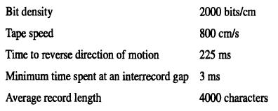
A tape drive has the following parameters:Estimate the percentage gain in time resulting from the ability to read records in both the forward and backward directions. Assume that records are accessed at random and that on average, the distance between two records accessed in sequence is four
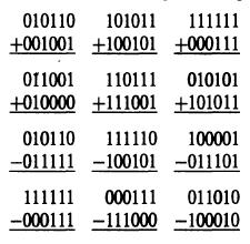
Consider the binary numbers in the following addition and subtraction problems to be signed, 6-bit values in the 2's-complement representation. Perform the operations indicated, specify whether or not arithmetic overflow occurs, and check your answers by converting operands and results to decimal
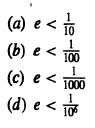
Signed binary fractions in 2's-complement representation are discussed at the beginning of Section 6.7. (a) Express the decimal values 0.5,-0.123, -0.75, and -0.1 as signed 6-bit fractions. (See Appendix E for decimal-to-binary fraction conversion.) (b) What is the maximum representation error,e,
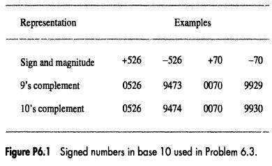
The 1's-complement and 2's-complement binary representation methods are special cases of the (b-1)'s-complement and b's-complement representation techniques in base b number systems. For example, consider the decimal system. The sign-and- magnitude values +526, -526, +70, and -70 have 4-digit
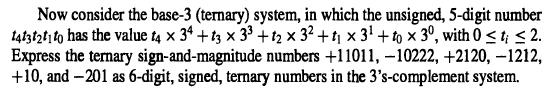
Represent each of the decimal values 56, -37, 122, and -123 as signed 6-digit numbers in the 3's-complement ternary format, perform addition and subtraction on them in all possible pairwise combinations, and state whether or not arithmetic overflow occurs for each operation performed. (See Problem
A half adder is a combinational logic circuit that has two inputs, x and y, and two outputs, s andc, that are the sum and carry-out, respectively, resulting from the binary addition of x and y. (a) Design a half adder as a two-level AND-OR circuit. (b) Show how to implement a full adder, as shown
Write a 68000 or IA-32 program to transform a 16-bit positive binary number into a 5-digit decimal number in which each digit of the number is coded in the binary-coded decimal (BCD) code. These BCD digit codes are to occupy the low-order 4 bits of five successive byte locations in the main memory.
Assume that four BCD digits, representing a decimal integer in the range 0 to 9999, are packed into the lower half of a 32-bit memory location DECIMAL. Write an ARM, 68000, or IA-32 subroutine to convert the decimal integer stored at DECIMAL into binary representation and to store it in the memory
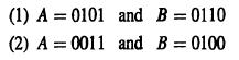
A modulo 10 adder is needed for adding BCD digits. Modulo 10 addition of two BCD digits, A = A3A2A1A and B = B3B2B Bo, can be achieved as follows: Add A to B (binary addition). Then, if the result is an illegal code that is greater than or equal to 1010, add 610. (Ignore overflow from this
Show that the logic expression CC-1 is a correct indicator of overflow in the addition of 2's-complement integers, by using an appropriate truth table.LO1
(a) Design a 64-bit adder that uses four of the 16-bit carry-lookahead adders shown in Figure 6.5 along with additional logic to generate C16, C32, C48, and C64, from co and the G and P variables shown in this figure. What is the relationship of the additional logic to the logic inside each
(a) How many logic gates are needed to build the 4-bit carry-lookahead adder shown in Figure 6.4? (b) Use appropriate parts of the result from Part (a) to calculate how many logic gates are needed to build the 16-bit carry-lookahead adder shown in Figure 6.5.LO1
Show that the worst case delay through an n x n array of the type shown in Figure 6.6b is 6(n-1) 1 gate delays, as claimed in Section 6.3.LO1
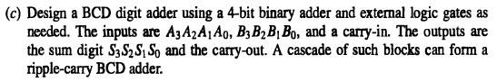
Showing 900 - 1000
of 1306
1
2
3
4
5
6
7
8
9
10
11
12
13
14
Step by Step Answers