New Semester
Started
Get
50% OFF
Study Help!
--h --m --s
Claim Now
Question Answers
Textbooks
Find textbooks, questions and answers
Oops, something went wrong!
Change your search query and then try again
S
Books
FREE
Study Help
Expert Questions
Accounting
General Management
Mathematics
Finance
Organizational Behaviour
Law
Physics
Operating System
Management Leadership
Sociology
Programming
Marketing
Database
Computer Network
Economics
Textbooks Solutions
Accounting
Managerial Accounting
Management Leadership
Cost Accounting
Statistics
Business Law
Corporate Finance
Finance
Economics
Auditing
Tutors
Online Tutors
Find a Tutor
Hire a Tutor
Become a Tutor
AI Tutor
AI Study Planner
NEW
Sell Books
Search
Search
Sign In
Register
study help
business
organization development
Computer Organization 5th Edition V Carl Hamacher, Carl Hamacher, Zvonko G Vranesic, Safwat G Zaky - Solutions
Give a general description of the hardware needed to support execution of the Alloc X,Y instruction used for managing the IA-64 register stack. Assume that small registers and adders are available. How are they used?
The Alpha 21264 processor has a much different arrangement of caches than the 21164. Why is the arrangement in the 21264 better? That is, under what circumstances do programs execute more quickly on the 21264, based only on the effects of cacheing? Include more than an observation on hit rates in
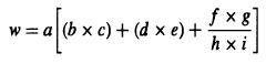
Show how the expressioncan be evaluated in an HP3000 computer. w= a[(bxc)+(de) + fx g hxi
In an HP3000 computer, Procedure, generates eight words of data, DI,..., DI8, which are stored in the stack. After these words are placed in the stack, but before the com- pletion of Procedure,, a new procedure, Procedure;, is called. It generates 10 words of data, DJ1,..., DJ10, which are also
Show how the expressioncan best be evaluated by the HP3000, ARM, Motorola 68000, and IA-32 computers. The values of variables w,a, b,c, d, and e are stored in memory locations. The following assumptions are made. The addresses do not reference successive locations. Direct memory addressing in the
What is the largest number of stack locations occupied during execution of the program in Figure 11.9?
Repeat Problem 11.16 for the HP3000 programs in Problems 11.13 and 11.15.LO1
Write a program loop whose instructions can be broadcast from the control processor in Figure 12.1 that will enable an array processor to iteratively compute temperatures in a plane, as discussed in Section 12.2. In addition to instructions that shift the network register contents between adjacent
Assume that a bus transfer takes T seconds and memory access time is 47 seconds. A read request over a conventional bus then requires 67 seconds to complete. How many conventional buses are needed to equal or exceed the bandwidth of a split- transaction bus that operates with the same time delays?
In a bus-based multiprocessor, the system bus can become a bottleneck if it does not support a high enough transfer rate. Suppose that a split-transaction bus is designed to be four times as wide as the word length of the processors used in the system. Will this increase the effective transfer rate
Assume that the cost of a 2 2 switch in a shuffle network is twice the cost of a crosspoint in a crossbar switch. There are n crosspoints in an n x n crossbar switch. As n increases, the crossbar becomes more costly than the shuffle network. What is the smallest value of n for which crossbar cost
Shuffle networks can be built from 4 x 4 and 8 x 8 switches, for example, instead of from 2x2 switches. Draw a 16 x 16 (n = 16) shuffle network built from 44 switches. If the cost of a 4 x 4 switch is four times the cost of a 2 2 switch, compare the cost of shuffle networks built from 4 x 4
Suppose that each procedure of a PAR segment (see Figure 12.14) requires 1 unit of time to execute. A program consists of three sequential segments. Each segment requires k time units and must be executed on a single processor. The three sequential segments are separated by two PAR segments, each
The shortest distance a message travels in an n-dimensional hypercube is 1 hop, and the longest distance a message needs to travel is n hops. Assuming that all possible source/destination pairs are equally likely, is the average distance a message needs to travel larger or smaller than (1 + n)/2?
A task that "busy-waits" on a lock variable by using a Test-and-Set instruction in a two-instruction loop, as in Figure 12.15, wastes bus cycles that could otherwise be used for computation. Suggest a way around this problem that involves a centralized queue of waiting tasks that is maintained by
What are the arguments for and against invalidation and updating as strategies for maintaining cache coherence?
Section 12.6.3 argues that cache coherence controls cannot replace the need for lock variables. Can the use of lock variables replace the need for explicit cache coherence controls?
Estimate the improvement in performance that can be achieved if the program in Fig- ure 12.19 is used rather than the program in Figure 12.18. Make some appropriate assumptions about the amount of time it takes to perform each step in the program.
Modify the program in Figure 12.19 to make it suitable for execution in a four-processor machine.
Modify the program in Figure 12.20 to make it suitable for execution in a four-processor system.
For small vectors, the approach in Figure 12.19 will be worse than if the dot product is computed using a single processor. Estimate the minimum size of the vectors for which this approach leads to better performance. Make some appropriate assumptions about the amount of time it takes to perform
Repeat Problem 12.14 for the approach in Figure 12.20.
Shared-memory multiprocessors and message-passing multicomputers are architec- tures that support simultaneous execution of tasks that interact with each other. Which of these two architectures can emulate the action of the other more easily? Briefly justify your answer.
The Ethernet bus LAN protocol is really only suitable when message transmission time is significantly larger than 2t, where r is the end-to-end bus propagation delay. Consider the case in which transmission time is less than T. Is it possible for a destination station to correctly receive an
A mailbox memory is a RAM memory with the following feature. A full/empty bit, F/E, is associated with each memory word location. The instructionis executed indivisibly as follows. The F/E bit associated with mailbox memory location BOXLOC is tested. If it is 0, denoting empty, then the contents of
Implement the COINCIDENCE function in sum-of-products form, where COINCIDENCE = XOR LO1
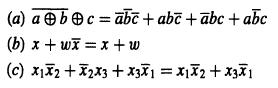
Prove the following identities by using algebraic manipulation and also by using truth tables.LO1 (a) abc abc + abc + abc + abc = (b) x+wx=x+w (c) x1x2+2x3 + x3x1 = x1x2+x31
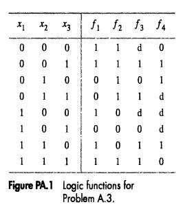
Derive minimal sum-of-products forms for the four 3-variable functionsf, f2, f3, and f4 given in Figure PA.1. Is there more than one minimal form for any of these functions? If so, derive all of them.LO1 f1 f2 f3 f4 0 0 0 1 1 d 0 0 0 1 1 1 1 1 0 1 0 10 1 0 1 1 0 1 1 d 1 00 1 0 d d 1 0 1 0 0 0 d 1
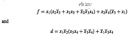
Find the simplest sum-of-products form for the function f using the don't-care conditiond, whereLO1 and d f = x1(x2x3 + x2x3 + x2x3x4) + x2x4(x3 + x1) d=x1x2(x3x4+3x4) + 1x3x4
Consider the function(a) Use a Karnaugh map to find a minimum cost sum-of-products (SOP) expression forf. (b) Find a minimum cost SOP expression for F, which is the complement off. Then, complement (using de Morgan's rule) this SOP expression to find an expression forf. The resulting expression
Find a minimum cost implementation of the function f(x1, x2, x3, x4), where f = 1 if either one or two of the input variables have the logic value 1. Otherwise, f = 0.LO1
Figure A.6 defines the 4-bit encoding of BCD digits. Design a circuit that has four inputs labeled b3, ..., bo, and an outputf, such that f = 1 if the 4-bit input pattern is a valid BCD digit; otherwise f = 0. Give a minimum cost implementation of this circuit.LO1
Two 2-bit numbers A = aao and B = bibo are to be compared by a four-variable function f(a, ao,b, bo). The function f is to have the value 1 wheneverwhere v(X) = x1 x21+xo x 2 for any 2-bit number. Assume that the variables A and B are such that v(A) - v(B)| 2. Synthesize f using as few gates as
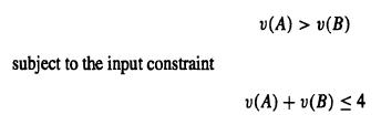
Repeat Problem A.8 for the requirement that f = 1 whenever.LO1 subject to the input constraint v(A) > v(B) v(A) + v(B) 4
Prove that the associative rule does not apply to the NAND operator.LO1
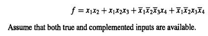
Implement the following function with no more than six NAND gates, each having three inputs.LO1 f=x1x2 + x1x2x3+X1x2x3x4 +12x34 Assume that both true and complemented inputs are available.
Show how to implement the following function using six or fewer two-input NAND gates. Complemented input variables are not available.LO1 f(x1+x3)(x2+x4)
Implement the following function as economically as possible using only NAND gates. Assume that complemented input variables are not available.LO1 f = (x1+x3)(x2+x4)
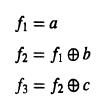
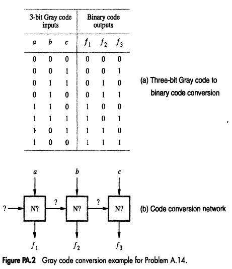
A number code in which consecutive numbers are represented by binary patterns that differ only in one bit position is called a Gray code. A truth table for a 3-bit Gray code to binary code converter is shown in Figure PA.2a. (a) Implement the three functions f1, f2, and f3 using only NAND gates.
Implement the XOR function using only 4 two-input NAND gates.
Figure A.37 defines a BCD to seven-segment display decoder. Give an implementation for this truth table using AND, OR, and NOT gates. Verify that the same functions are correctly implemented by the NAND gate circuits shown in the figure.LO1
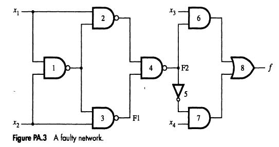
In the logic network shown in Figure PA.3, gate 3 fails and produces the logic value 1 at its output F1 regardless of the inputs. Redraw the network, making simplificationswherever possible, to obtain a new network that is equivalent to the given faulty network and that contains as few gates as
Figure A.16 shows the structure of a general CMOS circuit. Derive a CMOS circuit that implements the functionUse as few transistors as possible. (Hint: Consider series/parallel networks of transistors. Note the complementary series and parallel structure of the pull-up and pull-down networks in
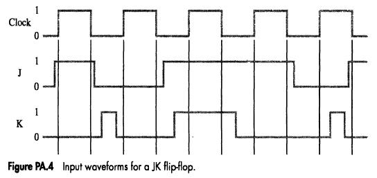
Draw the waveform for the output Q in the JK circuit of Figure A.31, using the input waveforms shown in Figure PA.4 and assuming that the flip-flop is initially in the O state.LO1 1 Clock 0 1 J 1 K 0 Figure PA.4 Input waveforms for a JK flip-flop.
Derive the truth table for the NAND gate circuit in Figure PA.5. Compare it to the truth table in Figure A.24b and then verify that the circuit in Figure A.26 is equivalent to the circuit in Figure A.25a.LO1
Compute both the setup time and the hold time in terms of NOR gate delays for the negative edge-triggered D flip-flop shown in Figure A.29.LO1
In the circuit of Figure A.27a, replace all NAND gates with NOR gates. Derive a truth table for the resulting circuit. How does this circuit compare with the circuit in Figure A.27a?LO1
Figure A.33 shows a shift register network that shifts the data to the right one place at a time under the control of a clock signal. Modify this shift register to make it capable of shifting data either one or two places at a time under the control of the clock and an additional control input
A 4-bit shift register that has two control inputs - INITIALIZE and RIGHT/LEFT- is required. When INITIALIZE is set to 1, the binary number 1000 should be loaded into the register independently of the clock input. When INITIALIZE = 0, pulses at the clock input should rotate this pattern. The
Derive a three-input to eight-output decoder network, with the restriction that the gates to be used cannot have more than two inputs.LO1
Figure A.35 shows a 3-bit up counter. A counter that counts in the opposite direction (that is, 7, 6, ..., 1, 0, 7, ...) is called a down counter. A counter capable of counting in both directions under the control of an UP/DOWN signal is called an up/down counter. Show a logic diagram for a 3-bit
Figure A.35 shows an asynchronous 3-bit up-counter. Design a 4-bit synchronous up- counter, which counts in the sequence 0, 1, 2, ..., 15, 0.... Use T flip-flops in your circuit. In the synchronous counter all flip-flops have to be able to change their states at the same time. Hence, the primary
A switching function to be implemented is described by the expression(a) Show an implementation off in terms of an eight-input multiplexer circuit. (b) Can f be realized with a four-input multiplexer circuit? If so, show how.LO1 f(x1, x2, x3, x4)=x1x3x4+1x3x4+X2X3X4
Repeat Problem A.28 forLO1 f(x1, x2, x3, x4)=x12x3 + x2x3x4 +14
(a) What is the total number of distinct functions, f(x1, x2, x3), of three binary variables? (b) How many of these functions are implementable with one PAL circuit of the type shown in Figure A.43? (c) What is the smallest change in the circuit in Figure A.43 that should be made to allow any
Consider the PAL circuit in Figure A.43. Suppose that the circuit is modified by adding a fourth input variable, x4, whose uncomplemented and complemented forms can be connected to all four AND gates in the same way as the variables x1, x2, and x3.(a) Can this modified PAL be used to implement the
Complete the design of the up/down counter in Figure A.47 by using the state assignment SO=10, $1 = 11, S2 = 01, and S3 = 00. How does this design compare with the one given in Section A.13.1?LO1
Design a 2-bit synchronous counter of the general form shown in Figure A.50 that counts in the sequence ..., 0, 3, 1, 2, 0, ..., using D flip-flops. This circuit has no external inputs, and the outputs are the flip-flop values themselves.LO1
Repeat Problem A.33 for a 3-bit counter that counts in the sequence ..., 0, 1, 2, 3, 4, 5,0,..., taking advantage of the unused count values 6 and 7 as don't-care conditions in designing the combinational logic.LO1
In Section A.13, D flip-flops were used in the design of synchronous sequential circuits. This is the simplest choice in the sense that the logic function values for a D input are directly determined by the desired next-state values in the state table. Suppose that JK flip-flops are to be used
Repeat Problem A.34 using JK flip-flops instead of D flip-flops. The general procedure for doing this is provided by the answer to Problem A.35.
Repeat Problem A.34 using JK flip-flops instead of D flip-flops. The general procedure for doing this is provided by the answer to Problem A.35.
In the vending machine example used in Section A.13.4 to illustrate the finite state machine model, a single binary output, z, was used to indicate the dispensing of mer- chandise. Change was not provided as an output. The purpose of this problem is to expand the output to include providing proper
Finite state machines can be used to detect the occurrence of certain subsequences in the sequence of binary inputs applied to the machine. Such machines are called finite state recognizers. Suppose that a machine is to produce a 1 as its output coincident with the second 1 in the pattern 011
Repeat Part a only of Problem A.38 for a machine that is to recognize the occurrence of either of the subsequences 011 and 010 in the input sequence, including the cases where overlap occurs. For example, the input sequence 110101011... is to produce the output sequence 000010101....LO1
Why is the Wait-for-Memory-Function-Completed step needed when reading from or writing to the main memory?LO1
A processor uses a control sequence similar to that in Figure 7.6. Assume that a memory read or write operation takes the same time as one internal processor step and that both the processor and the memory are controlled by the same clock. Estimate the execution time of this sequence.LO1
Repeat Problem 7.2 for a machine in which the memory access time is equal to twice the processor clock period.LO1
Assume that propagation delays along the bus and through the ALU of Figure 7.1 are 0.3 and 2 ns, respectively. The setup time for the registers is 0.2 ns, and the hold time is 0. What is the minimum clock period needed?LO1
Write the sequence of control steps required for the bus structure in Figure 7.1 for each of the following instructions: (a) Add the (immediate) number NUM to register R1. (b) Add the contents of memory location NUM to register R1. (c) Add the contents of the memory location whose address is at
The three instructions in Problem 7.5 have many common control steps. However, some of these control steps occur at different counts of the control step counter. Suggest a scheme that exploits these common steps to reduce the complexity of the encoder block in Figure 7.11.LO1
Consider the Add instruction that has the control sequence given in Figure 7.6. The processor is driven by a continuously running clock, such that each control step is 2 ns in duration. How long will the processor have to wait in steps 2 and 5, assuming that a memory read operation takes 16 ns to
The addressing modes of a 32-bit, byte-addressable machine include autoincrement and autodecrement. In these modes, the contents of an address register are either incre- mented or decremented by 1, 2, or 4, depending on the length of the operand. Suggest some modification to Figure 7.1 to simplify
Show a possible control sequence for implementing the instruction MUL R1, R2 on the processor in Figure 7.1. This instruction multiplies the contents of the registers R1 and R2, and stores the result in R2. Higher-order bits in the product, if any, are discarded. Suggest additional control signals
Show the control steps for the Branch-on-Negative instruction for a processor that has the structure given in Figure 7.8.LO1
Show the control steps needed to implement the Branch-to-Subroutine instruction of one of the processors described in Chapter 3. Assume that processor has the internal organization of Figure 7.1.LO1
Repeat Problem 7.11 for the processor in Figure 7.8.LO1
Figure 7.3 shows an edge-triggered flip-flop being used for implementing the processor registers. Consider the operation of transferring data from one register to another. Examine the timing of this operation in detail and explain any potential difficulties that may be encountered if the
The multiplexer and feedback connection in Figure 7.3 eliminate the need for gating the clock input as a means for enabling and disabling register input. Using a timing diagram, explain the problems that may arise if clock gating were used.LO1
Assume that the register file in Figure 7.8 is implemented as a RAM. At any given time, a location in this RAM can be accessed for either a read or a write operation. During the operation R1 [R1] + [R2], register R1 is both a source and a destination. Explain how you would use additional latches at
The Run signal in Figure 7.11 is set to 0 to prevent the control step counter from being advanced while waiting for a memory read or write operation to be completed. Examine the timing diagram in Figure 7.5, and prepare a state diagram for a control circuit that generates this signal. Design an
The MDR in E control signal is asserted following a clock cycle in which the control signal Read is asserted and is negated when the memory transfer is completed, as shown in Figure 7.5. Design a suitable circuit to generate MDR.inE LO1
Consider a 16-bit, byte-addressable machine that has the organization of Figure 7.1. Bytes at even and odd addresses are transferred on the high- and low-order 8 bits of the memory bus, respectively. Show a suitable gating scheme for connecting register MDR to the memory bus and to the internal
Design an oscillator using an inverter and a delay element. Assuming that the delay element introduces a delay T, what is the frequency of oscillation? Modify the oscillator circuit such that oscillations can be started and stopped under the control of an asynchronous input RUN. When the oscillator
Some control steps in a processor take longer to complete than others. It is desired to generate a clock signal controlled by a signal called Long/Short such that the duration of a control step is twice as long when this signal is equal to 1. Assume that the control step counter has an Enable input
The output of a shift register is inverted and fed back to its input, to form a counting circuit known as a Johnson counter. (a) What is the count sequence of a 4-bit Johnson counter, starting with the state 0000? (b) Show how you can use a Johnson counter to generate the timing signals T1, T2, and
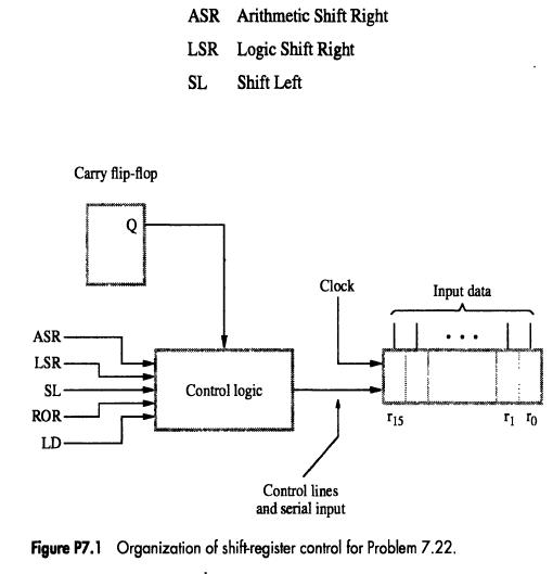
An ALU of a processor uses the shift register shown in Figure P7.1 to perform shift and rotate operations. Inputs to the control logic for this register consist ofAll shift and load operations are controlled by one clock input. The shift register is implemented with edge-triggered D flip-flops.
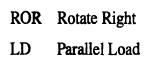
The digital controller in Figure P7.2 has three outputs, X, Y, and Z, and two inputs, A and B. It is externally driven by a clock. The controller is continuously going through the following sequence of events: At the beginning of the first clock cycle, line X is set to 1. At the beginning of the
Write a microroutine, such as the one shown in Figure 7.21, for the instruction MOV X(Rsrc), Rdst where the source and destination operands are specified in indexed and register ad- dressing modes, respectively.LO1
A BGT (Branch if > 0) machine instruction has the expression Z + (NV) = 0 as its branch condition, where Z, N, and V are the zero, negative, and overflow condition flags, respectively. Write a microroutine that can implement this instruction. Show the circuitry needed to test the condition codes.LO1
Write a combined microroutine that can implement the BGT (Branch if > 0), BPL (Branch if Plus), and BR (Branch Unconditionally) instructions. The branch conditions for the BGT and BPL instructions are Z + (NV) = 0 and N = 0, respectively. What is the total number of microinstructions required? How
Figure 7.21 shows an example of a microroutine in which bit-ORing is used to modify microinstruction addresses. Write an equivalent routine, without using bit-ORing, in which conditional branch microinstructions are used. How many additional microin- structions are needed? Assume that the
Show how the microprogram in Figure 7.20 should be modified to implement the 68000 microprocessor instruction ADD src, Rdst LO1
Explain how the flowchart in Figure 7.20 can be modified to implement the general instruction MOVE src,dst in which both the source and the destination can be in any of the five address modes shown.LO1
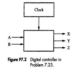
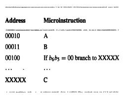
Figure P7.3 gives part of the microinstruction sequence corresponding to one of the machine instructions of a microprogrammed computer. Microinstruction B is followedby C, E, F, or I, depending on bits b6 and bs of the machine instruction register. Compare the three possible implementations
It is desired to reduce the number of bits needed to encode the control signals in Figure 7.19. Suggest a new encoding that reduces the number of bits by two. How does the new encoding affect the number of control steps needed to implement an instruction?LO1
Suggest a new encoding for the control signals in Figure 7.19 that reduces the number of bits needed in a microinstruction to 12. Show the effect of the new encoding on the control sequences in Figures 7.6 and 7.7.LO1
Suggest a format for microinstructions, similar to Figure 7.19, if the processor is orga- nized as shown in Figure 7.8.LO1
What are the relative merits of horizontal and vertical microinstruction formats? Relate your answer to the answers to Problems 7.31 and 7.32.LO1
What are the advantages and disadvantages of hardwired and microprogrammed control?LO1
Showing 700 - 800
of 1306
1
2
3
4
5
6
7
8
9
10
11
12
13
14
Step by Step Answers