New Semester
Started
Get
50% OFF
Study Help!
--h --m --s
Claim Now
Question Answers
Textbooks
Find textbooks, questions and answers
Oops, something went wrong!
Change your search query and then try again
S
Books
FREE
Study Help
Expert Questions
Accounting
General Management
Mathematics
Finance
Organizational Behaviour
Law
Physics
Operating System
Management Leadership
Sociology
Programming
Marketing
Database
Computer Network
Economics
Textbooks Solutions
Accounting
Managerial Accounting
Management Leadership
Cost Accounting
Statistics
Business Law
Corporate Finance
Finance
Economics
Auditing
Tutors
Online Tutors
Find a Tutor
Hire a Tutor
Become a Tutor
AI Tutor
AI Study Planner
NEW
Sell Books
Search
Search
Sign In
Register
study help
computer science
systems analysis design
The Analysis And Design Of Linear Circuits 10th Edition Roland E. Thomas, Albert J. Rosa, Gregory J. Toussaint - Solutions
A balanced three-phase load has a phase impedance of \(Z_{\Delta}=300-j 600 \Omega /\) phase. The line voltage at the load is \(V_{\mathrm{L}}=\) \(2.4 \mathrm{kV}\) (rms).(a) Convert the \(\Delta\) load into a \(Y\) load.(b) Find \(I_{\mathrm{L}}\) and the complex power delivered to the load.(c)
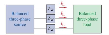
In the balanced three-phase system in Figure P16-42 the line and load impedances are \(Z_{\mathrm{W}}=2+j 12 \Omega /\) phase and \(Z_{\mathrm{Y}}=\) \(16+j 10 \Omega /\) phase. The line current is \(I_{\mathrm{L}}=15 \mathrm{~A}(\mathrm{rms})\). Find \(V_{\mathrm{L}}\) at the source and the
In the balanced three-phase circuit in Figure P16-42, the line impedance is \(Z_{\mathrm{W}}=5+j 30 \Omega /\) phase. The apparent power delivered to the load is \(25 \mathrm{kVA}\) at a lagging power factor of 0.85 . The line current is \(I_{\mathrm{L}}=12 \mathrm{~A}(\mathrm{rms})\). Find the
As a young engineer working for a consulting company, your supervisor gives you the Multisim circuit shown in Figure P16-45. She asks you to improve the complex power being delivered to the three-phase load by increasing the power factor to as close to 1 as possible. The manufacturer of the load
Two balanced three-phase loads are connected in parallel. The first load absorbs \(25 \mathrm{~kW}\) at a lagging power factor of 0.9. The second load absorbs an apparent power of \(30 \mathrm{kVA}\) at a leading power factor of 0.1. The line voltage at the parallel loads is \(V_{\mathrm{L}}=88
The average power delivered to a balanced Y-connected load is \(20 \mathrm{~kW}\) at \(60 \mathrm{~Hz}\) at a lagging power factor of 0.8 . The line voltage at the load is \(V_{\mathrm{L}}=480 \mathrm{~V}(\mathrm{rms})\).(a) Find the phase impedance \(Z_{Y}\) of the load.(b) Change the load so that
The apparent power delivered to a balanced \(\Delta\)-connected load is \(25 \mathrm{kVA}\) at a lagging power factor of 0.72 . The line voltage at the load is \(V_{\mathrm{L}}=20 \mathrm{kV}\) (rms). Find the phase impedance \(Z_{\Delta}\) of the load.
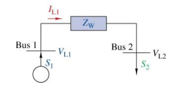
In Figure P16-4.9, the source and load buses are interconnected by a transmission line with \(Z_{\mathrm{W}}=40+j 280\) \(\Omega /\) phase. The load at bus 2 draws an apparent power of \(\left|S_{2}ight|=\) 3 MVA at a leading power factor of 0.8 and the line voltage at bus 2 is \(V_{\mathrm{L}
In Figure P16-4.9, the source and load buses are interconnected by a transmission line with wire impedance \(Z_{\mathrm{W}}\). The load at bus 2 draws an average power of \(P_{2}=600 \mathrm{~kW}\) at a lagging power factor of 0.85 and the line current is \(I_{\mathrm{L} 1}=10 \mathrm{~A}\) (rms).
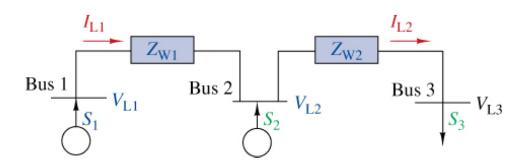
In Figure P16-51, the three buses are interconnected by transmission lines with wire impedances of \(Z_{\mathrm{W}_{1}}=100+j\) \(600 \Omega /\) phase and \(Z_{\mathrm{W}_{2}}=120+j 800 \Omega /\) phase. The source at bus 2 produces an apparent power of \(\left|S_{2}ight|=300 \mathrm{kVA}\) at a
In Figure P16-53, the source at bus 1 supplies two load buses through transmission lines with wire impedances of \(Z_{\mathrm{W}_{1}}=6+j 33 \Omega /\) phase and \(Z_{\mathrm{W}_{2}}=3+j 15 \Omega /\) phase. The load at bus 2 draws an apparent power 4 MVA at a lagging power factor of 095. The load
In a balanced three-phase system \(\mathbf{V}_{\mathrm{AN}}=V_{\mathrm{P}}
The power factor of a \(50-\mathrm{hp}(1 \mathrm{hp}=746 \mathrm{~W})\) three-phase induction motor is 0.8 when it delivers its rated mechanical output. When delivering its rated output, the motor efficiency is \(90 \%\). Find the \(\mathrm{kVA}\) rating of the motor.
A balanced three-phase source and a balanced three-phase load are interconnected by a three-phase transmission line. The load draws an average power of \(P_{\mathrm{L}}=45 \mathrm{~kW}\) at a lagging power factor of 0.8 and the source produces a complex power of \(S_{\mathrm{S}}=(45 \cdot 2+j\)
Consider the Multisim representation of a balanced three-phase Y-Y power system shown in Figure P16-57. An owner of the plant who wants to install the system is contemplating whether to save money by eliminating the need for the neutral return line. The owner (not an engineer) was told that the
Find the \(z\)-parameters of the two-port network in Figure P17-1 . Validate your results using Multisim. 1 + 400 V, 400 16 400 400 V 19
Find the \(z\)-parameters of the two-port network in Figure P17-2 and provide the results in matrix form. Is the circuit reciprocal? Validate your results using Multisim. w + 1 2 ww 1 1 V2 +
Find the \(y\)-parameters of the two-port network in Figure P17=3 . Validate your results using Multisim. Use \(60 \mathrm{~Hz}\).
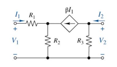
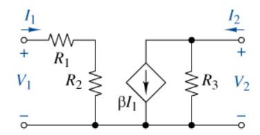
(a) Find the \(z\)-parameters of the two-port network in Figure P17-4.(b) If \(\beta=50\), select values of the resistors so that \(Z_{\mathrm{IN}}=52\) \(\mathrm{k} \Omega\). + V 16 R www R BI R3 ww 9+ V 19
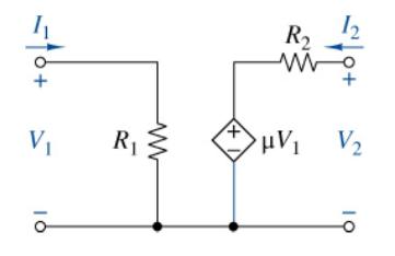
Figure P17-6 is a simplified model of a voltage amplifier. The \(z\)-parameter matrix of the model is \([\mathbf{z}]=\left[\begin{array}{cc}100 \mathrm{k} \Omega & 0 \\ 10 \mathrm{M} \Omega & 1 \mathrm{k} \Omega\end{array}ight]\). gain parameter \(\mu\) that will match the \(z\)-matrix. V
The \(y\)-parameters of a two-port circuit are \(y_{11}=6 \mathrm{mS}\), \(y_{12}=y_{21}=-2 \mathrm{mS}\), and \(y_{22}=2 \mathrm{mS}\). A 10-V voltage source is connected at the input port and a short circuit is connected across the output port. Find the port variable responses \(I_{1}\) and \(I\)
The \(y\)-parameters of a two-port circuit are \(y_{11}=20+j 20\) \(\mathrm{mS}, y_{12}=y_{21}=100-j 20 \mathrm{mS}\), and \(y_{22}=40+j 20 \mathrm{mS}\). Find the short-circuit ( \(V_{2}=0\) ) current gain \(T_{\mathrm{I}}=I_{2} / I_{1}\).
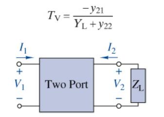
Figure P17-9., a load impedance \(Z_{\mathrm{L}}\) is connected across the output port. Show that the voltage gain \(T_{\mathrm{V}}=V_{2} / V_{1}\) is TO + = 16 V -Y21 YL + y22 Tv=- Two Port + 10 V ZL
Find the A-parameters of the two-port networks in Figure \(\underline{\text { P17-10. }}\). 19+ ~ = 16+ Y 10+ 10 (a) 19 + 19 Z 10+ 10 (b)
Find the \(t\)-parameters of the two-port network in Figure P17-10. -TO+16 V TO+16 V Y (a) Z (b) 19+ V 19 V IQ
(a) Find the \(t\)-parameters of the two-port network in Figure P17-12.(b) Select values of \(R_{1} R_{2}, R_{3}\), and \(\beta\), so that the following are achieved: \(T_{\mathrm{I}}=75, Z_{\mathrm{IN}}=2 \mathrm{k} \Omega\), and \(Z_{\mathrm{OUT} \mid \mathrm{V} 1=0}\) \(=100 \mathrm{k} \Omega\).
Find the \(t\)-parameters of the two-port network in Figure P17-12.
Find the \(h\)-parameters of the two-port network in Figure P17-14. it= V R 91 R + V 19
(a) The \(h\)-parameters of a two-port network are \(h_{11}=500\) \(\Omega, h_{12}=1, h_{21}=-1\), and \(h_{22}=2 \mathrm{mS}\). Find the Thévenin equivalent circuit at the output port when a \(20-\mathrm{V}\) voltage source is connected at the input port.(b) Connect a load \(R_{\mathrm{L}}\)
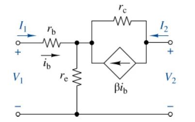
(a) A model of a BJT (bipolar junction transistor) in a common-emitter mode is shown in Figure P17-16. Find the \(h\)-parameters for this particular circuit.(b) Simplify your results if \(r_{\mathrm{C}} ightarrow \infty\). rb www lb www V V2 re Bib 19
The \(t\)-parameters of a two-port network are \(A=2, B\) \(=100 \Omega, C=3 \mathrm{mS}\), and \(D=1\).(a) Find the output resistance \(V_{2} / I_{2}\) when the input port is short-circuited.(b) Find the output resistance \(V_{2} / I_{2}\) when the input port is open-circuited.
The t-parameters of a two-port network are \(A=0, B=-j\) \(25 \Omega, C=-j 20 \mathrm{mS}\), and \(D=0.5-j 0.5\). Find the voltage gain \(V_{2}\) \(/ V_{1}\) when a \(500-\Omega\) load resistor is connected across the output port.
When a voltage \(V_{\mathrm{x}}\) is applied across the input port, the short-circuit current at the output port is \(I_{2 S C}\). When the same voltage is applied across the output port, the short-circuit current at the input port is \(I_{1 \mathrm{SC}}\). Show that reciprocity \(\left(I_{1
Starting with the \(h\)-parameter \(i-v\) relationships in Eq. (17-9), show that\[A=-\Delta_{h} / h_{21}, B=-h_{11} / h_{21}, C=-h_{22} / h_{21}, \text { and } D=-1 / h_{21}\]where \(\Delta_{h}=h_{11} h_{22}-h_{12} h_{21}\).
Starting with the \(t\)-parameter \(i-v\) relationships in Eq. (17-13), show that\[y_{11}=D / B, \quad y_{12}=-\Delta_{t} / B, \quad y_{21}=-1 / B, \quad \text { and } y_{22}=A / B\]where \(\Delta_{\mathrm{t}}=A D-B C\).
Starting with the \(h\)-parameter \(i-v\) relationships in \(\mathrm{Eq}\). (17-9), determine the voltage transfer function \(T_{\mathrm{V}}=V_{2} / V_{1}\) in terms of the \(h\)-parameters, when the output is open circuited.
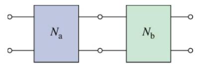
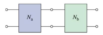
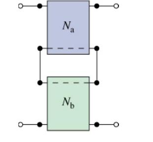
The \(t\)-parameters of the two-port networks \(N_{\mathrm{a}}\) and \(N_{\text {b }}\) in Figure P17-23 are\[\left[\boldsymbol{t}_{\mathrm{a}}ight]=\left[\begin{array}{rr}40 & 15 \\5 & 40\end{array}ight] \text { and }\left[\boldsymbol{t}_{\mathrm{b}}ight]=\left[\begin{array}{cc}5 & 2
The cascade connection in Figure P17-23 is a twostage amplifier with identical two-port stages each having the hh parameters h11=1.5kΩ,h12=0,h21=−20h11=1.5kΩ,h12=0,h21=−20, and h22=0.5mSh22=0.5mS. Find the tt-parameters of the cascade connection and then calculate the current gain of the
Find the voltage gain of the two-stage amplifier defined in Problem 17-25.Data From Problem 17-25ans 17-25 The cascade connection in Figure P17-23 is a twostage amplifier with identical two-port stages each having the \(h\) parameters \(h_{11}=1.5 \mathrm{k} \Omega, h_{12}=0, h_{21}=-20\), and
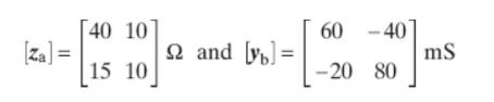
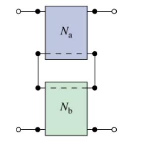
The two-port parameters of the series connection in Figure P17-27 areFind the \(z\)-parameters of the series connection. Is the network reciprocal? 40 10 15 10 60-40 -20 80 2 and [y] = []=[-20 mS
In Figure 17-27, the network \(N_{\mathrm{a}}\) is an active device with \(h\)-parameters \(h_{11}=10 \mathrm{k} \Omega, h_{12}=0, h_{21}=-5 \times 10^{3}\), and \(h\) \({ }_{22}=50 \mathrm{mS}\). The network \(N_{\mathrm{b}}\) is a resistive feedback circuit with \(z\) -parameters \(z_{11}=2 R\)
A two-port network is said to be unilateral if excitation applied at the input port produces a response at the output port, but the same excitation applied at the output port produces no response at the input port. Show that a two-port network is unilateral if \(A D-B C=0\)
A load impedance \(Z_{\mathrm{L}}\) is connected at the output of a two-port network. Show that the input impedance \(Z_{\mathrm{IN}}=V_{1} / I_{1}=Z_{\mathrm{L}}\) when \(A=D\) and \(C=B /\left(Z_{\mathrm{L}}ight)^{2}\).
The \(y\)-parameters of a two-port network operating in the sinusoidal steady state are \(y_{11}=20-j 15 \mathrm{mS}, y_{12}=y_{21}=-j 12\) \(\mathrm{mS}\), and \(y_{22}=10-j 20 \mathrm{mS}\). The input port is driven by an ac voltage. Design an output port load impedance \(Z_{\mathrm{L}}\) that
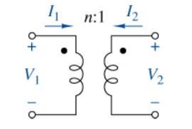
Some two-port networks do not have either \(z\) or \(y\) parameters. A good example is the ideal transformer shown in Figure P17-32. The equations defining this two-port network were found in Chapter 15 as\[\begin{gathered}V_{1}=n V_{2} \\I_{1}=-\frac{1}{n} I_{2}\end{gathered}\]Attempt to find the
Design an active high-pass filter to meet the specification in Problem 14-39. Use Multisim to verify that your design meets the specifications.Data From Problem 14-39Construct the lowest order, high-pass transfer functions that meet the following filter specifications. Calculate the gain (in
Design an active high-pass filter to meet the specification in Problem 14-40. Use Multisim to verify that your design meets the specifications.Data From Problem 14-40Construct the lowest order, high-pass transfer functions that meet the following filter specifications. Calculate the gain (in
Consider the specifications given in Problem 14-42.(a) Design an active Butterworth filter to meet the specification.(b) Design an active Chebyshev filter to meet the specification.(c) Use Multisim to verify that both your designs meet the specifications.(d) Comment on the pros and cons of each
A certain instrumentation system for a new hybrid car needs a bandpass filter to limit its output bandwidth prior to digitization. The filter must meet the following specifications:\[\begin{array}{ll}T_{\mathrm{MAX}}=+20 \pm 1 \mathrm{~dB} \omega_{\mathrm{CH}}=5.5 \mathrm{krad} / \mathrm{s}(875.4
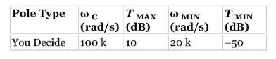
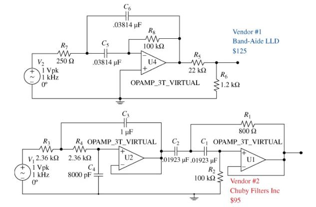
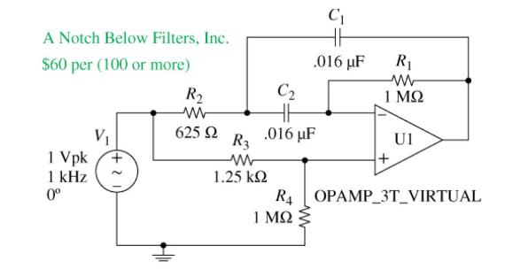
You are working at an aircraft manufacturing plant on an altitude sensor that eventually will be used to retrofit dozens of similar sensors on an upgrade to a current airframe. You are required to find a quality notch filter to eliminate an undesirable interference at \(400 \mathrm{~Hz}\). You find
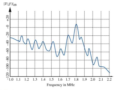
An amplified portion of the radio spectrum is shown in Figure P14-4 8 . You need to hear all of the signals from 1.0 to 2.0 MHz, but there is an interfering signal at 1.8 MHz. Design a notch filter to reduce that signal by at least \(50 \mathrm{~dB}\) and not reduce the desired signal at \(1.7
The portion of the radio spectrum known as the AM broadcast band ranges from \(540 \mathrm{kHz}\) to \(1700 \mathrm{kHz}\). You want to design a suitable filter and amplifier. The passband gain desired is \(80 \mathrm{~dB}\) and the "shoulders" of your filter should have a roll-off of \(-100
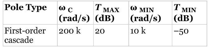
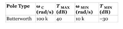
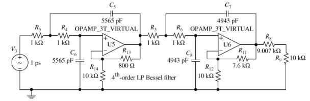
Bessel filters are in the category of maximally flat filters similar to Butterworth but have a critically damped time-domain response similar to a First-Order Cascade filter. Bessel filters have a linear phase response over the filter's passband, which makes them useful in audio applications.
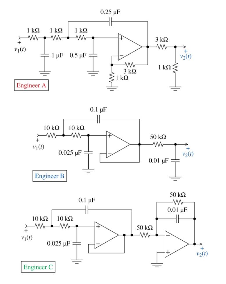
You are the head engineer for a small start-up and a client asked for a filter with the following specifications: a third-order Butterworth low-pass filter with a cutoff frequency of \(2 \mathrm{krad} / \mathrm{s}\) and a dc gain of o dB. Three of your junior engineers were tasked to design the
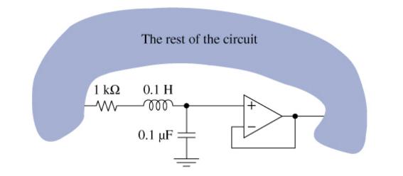
One of your company's products includes the passive \(R L C\) filter and OP AMP buffer circuit in Figure P14=52. The supplier of the inductor is no longer in business and a suitable replacement is not available, even on eBay, Amazon, or Craig's List. You have been asked to design a suitable
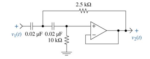
Ten years after earning a BSEE, you return for a master's degree and sign on as the laboratory instructor for the basic circuit analysis course. One experiment asks the students to build the active filter in Figure P14=53 and measure its gain response over the range from \(150 \mathrm{~Hz}\) to
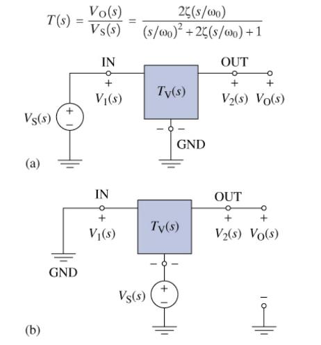
The three-terminal circuit in Figure P14=54. (a) has a bandpass transfer function of the formShow that the circuit in Figure P14=54 (b) has a bandstop transfer function of the form\[T(s)=\frac{V_{\mathrm{O}}(s)}{V_{\mathrm{S}}(s)}=\frac{\left(s / \omega_{0}ight)^{2}+1}{\left(s /
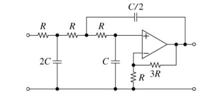
Show that the circuit in Figure P14=55 produces a third-order Butterworth low-pass filter with a cutoff frequency of \(\omega_{\mathrm{C}}=1\) / \(R C\) and a passband gain of \(K=4\). Then, design a third-order Butterworth low-pass filter using the filter in Figure P14=55 with a cutoff frequency
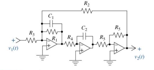
A biquad filter has the unique properties of having the ability to alter the filter's parameters, namely, gain \(K\), quality factor \(Q\), and resonant frequency \(\omega_{0}\). This is done in each case by simply adjusting one of the circuit's resistors. Furthermore, adjusting any of the three
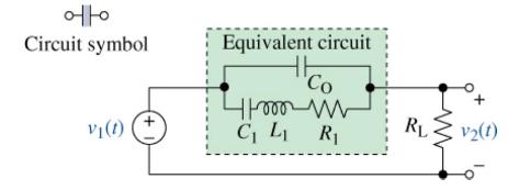
Although not an active filter, crystal (Quartz) filters are very high \(-Q\) filters. Some can have \(Q\) 's approaching 100,000. High \(Q\) means high selectivity; hence, crystal filters are used extensively in communications where fine-tuning is essential. In its simplest form, a quartz crystal
A scientist has a need for a bandpass filter for an Amateur Satellite band in the HF frequency band. It must have a center frequency of \(89.4 \mathrm{Mrad} / \mathrm{s}\) and a \(32 \mathrm{Mrad} / \mathrm{s}\) bandwidth. It must have a \(-85 \mathrm{~dB}\) per decade roll-off on both shoulders to
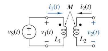
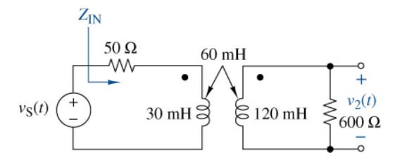
In Figure P15-1, \(L_{1}=10 \mathrm{mH}, L_{2}=50 \mathrm{mH}, k=0.4\) and \(v_{\mathrm{S}}(t)=200 \sin 100 t \mathrm{~V}\).(a) Write the \(i-v\) relationships for the coupled inductors using the reference marks in the figure.(b) Solve for \(v_{2}(t)\) when the output terminals are open circuited (
In Figure P15-1, \(L_{1}=10 \mathrm{mH}, L_{2}=5 \mathrm{mH}, M=7 \mathrm{mH}\), and \(v\) \(\mathrm{S}(t)=100 \sin 1000 t \mathrm{~V}\).(a) Write the \(i-v\) relationships for the coupled inductors using the reference marks in the figure.(b) Solve for \(i_{1}(t)\) and \(i_{2}(t)\) when the output
In Figure P1 5-1 \(, L_{1}=10 \mathrm{mH}, L_{2}=5 \mathrm{mH}, M=7 \mathrm{mH}\), and the outputs are \(v_{2}(t)=0\) and \(i_{2}(t)=35 \sin 1000 t \mathrm{~A}\).(a) Write the \(i-v\) relationships for the coupled inductors using the reference marks given.(b) Solve for the source voltage
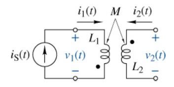
In Figure P15-4, \(L_{1}=L_{2}=5 \mathrm{mH}, M=2 \mathrm{mH}, k=0.4\), and \(i_{\mathrm{S}}(t)=120 \sin 377 t \mathrm{~A}\).(a) Solve for \(v_{1}(t)\) and \(v_{2}(t)\) when the output terminals are open circuited ( \(\left.i_{2}(t)=0ight)\).(b) Find the Thévenin Equivalent looking into the output
In Figure P15-4, \(L_{1}=L_{2}=4 \mathrm{mH}, M=3 \mathrm{mH}\), and \(i_{2}(\) \(t)=10 \sin 1000 t \mathrm{~mA}\) when the output terminals are short circuited. Solve for \(v_{1}(t)\) and \(i_{1}(t)\).
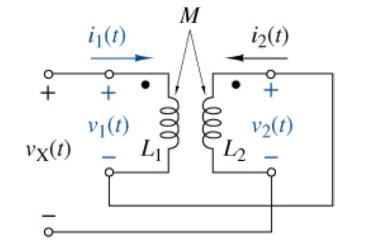
In Figure P15-6, \(L_{1}=2 \mathrm{H}, L_{2}=6 \mathrm{H}, M=3 \mathrm{H}\), and \(v_{\mathrm{X}}(\) \(t)=70 \cos (1000 t) \mathrm{V}\). Find the input current \(i_{1}(t)\) and the voltages \(v_{1}(t)\) and \(v_{2}(t)\) using Multisim. 6 + (1)XA 16 i(1) V1 (1) M ooo i(1) v(t) 12
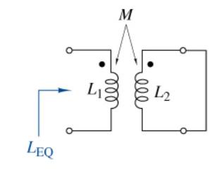
ans 15-7 In Figure P15-7 show that \(L_{\mathrm{EQ}}=L_{1}\left(1-k^{2}ight)\), where \(k\) is the coupling coefficient. LEQ M 100 L2
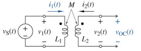
In Figure P15-8 show that the indicated open-circuit voltage is\[v_{\mathrm{OC}}=\left(k \sqrt{L_{2} / L_{1}}ight) v_{1}\]where \(k\) is the coupling coefficient. i(1) Mi(1) vs(t) + v(1) la L 42 + V2(1) v(t) + Voc(1)
Because of the numerous windings, transformers are likely to have a parasitic resistance associated with each coil.Figure P15-9. shows a pair of coupled coils with a series resistance associated with each inductance. Rewrite \(\mathrm{Eq}_{-}(15-12)\). to include the effects of the parasitic
A perfectly coupled (ideal) transformer is used to provide electricity to a \(1-\mathrm{k} \Omega, 12-\mathrm{V}\) doorbell from house voltage 169.7 sin \(377 t \mathrm{~V}\). Design the transformer's turn-ratio to meet this requirement. Then validate your design using Multisim. Assume additive
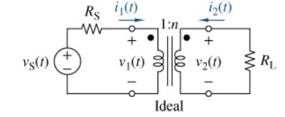
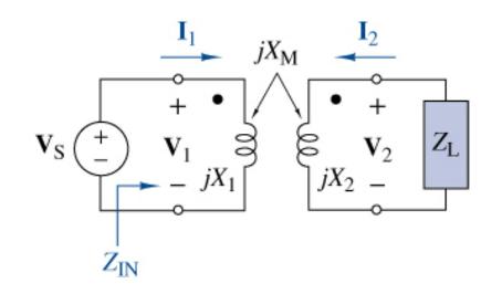
In Figure \(\mathrm{P} 15-11 R_{\mathrm{S}}=50 \Omega, R_{\mathrm{L}}=1250 \Omega\), the turns ratio is \(n=5\), and the source voltage is \(v_{\mathrm{S}}(t)=240 \cos\) \(377 t \mathrm{~V}\). Find expressions for \(i_{1}(t)\) and \(i_{2}(t)\). Validate your answer using Multisim. Vs(t) (+1) Rs
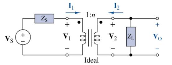
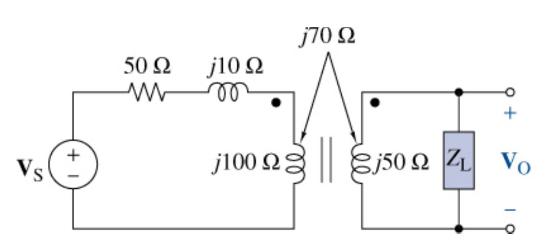
The turns ratio of the ideal transformer in Figure P \(15-12\) is \(n=10\). The source and load impedances are \(Z_{\mathrm{S}}=50 \Omega\) and \(Z_{\mathrm{L}}=\) \(500-j 500 \Omega\). Find \(\mathbf{I}_{1}, \mathbf{I}_{2}\), and \(V_{\mathrm{O}}\) when \(V_{\mathrm{S}}=200 Vs + Zs V el 1:n Ideal
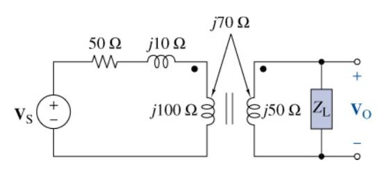
Design the turns ratio of the ideal transformer in Figure P15-12 so that \(\mathbf{V}_{\mathrm{O}}=708
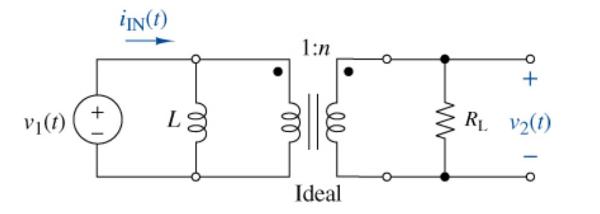
In Figure P15-14, the turns ratio is \(n=5, L=120 \mathrm{mH}\), and \(R_{\mathrm{L}}=1.5 \mathrm{k} \Omega\). Find \(i_{\mathrm{IN}}(t)\) and \(v_{2}(t)\) when \(v_{1}(t)=100\)\(\sin 377 t \mathrm{~V}\). Use Multisim to verify your results. Vj(t) + iIN(1) L 1:n Ideal ww R V(1)
(a) Design the turns ratio in Figure P15-14 if \(\mathbf{V}_{1}=100
The primary voltage of an ideal transformer used in a home furnace to connect to a thermostat is a \(120-\mathrm{V}, 60-\mathrm{Hz}\) sinusoid. The secondary voltage is a \(24-\mathrm{V}, 60-\mathrm{Hz}\) sinusoid. The secondary winding is connected to a \(150-\Omega\) resistive load thermostat.(a)
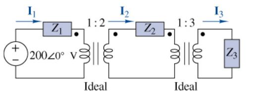
In Figure P15-17 the impedances are \(Z_{1}=20-j 45\) \(\Omega, Z_{2}=45+j 30 \Omega\), and \(Z_{3}=300+j 250 \Omega\). Find \(\mathbf{I}_{1}, \mathbf{I}_{2}\), and \(\mathbf{I}\) 3. + Z 20020 V 1:2 Ideal 1 Z2 1:3 Ideal Z3
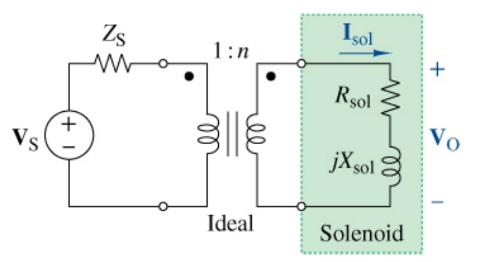
The solenoid in Figure P15-18 needs \(24 \mathrm{~V}\) to operate properly. The source \(\mathbf{V}_{\mathrm{S}}=170 S +1 Zs ww 1:n 3118 Ideal Isol Rsol jXsol Solenoid Vo
The primary winding of an ideal transformer with \(N_{1}\) \(=100\) and \(N_{2}=250\) is connected to a \(480-\mathrm{V}\) source. A \(1-\mathrm{k} \Omega\) load is connected across the secondary windings. Find amplitudes of the primary and secondary currents.
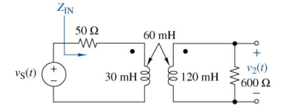
The input voltage to the transformer in Figure \(\mathrm{P} 15-20\) is a \(\operatorname{sinusoid} v_{\mathrm{S}}(t)=339 \sin (314 t) \mathrm{V}\). With the circuit operating in the sinusoidal steady state, transform the circuit into the phasor domain and write mesh-current equations. Solve for the
Repeat Problem 15-20 with \(v_{\mathrm{S}}(t)=10 \cos 2000 t \mathrm{~V}\).Data From Problem 15-2015-20 The input voltage to the transformer in Figure \(\mathrm{P} 15-20\) is a \(\operatorname{sinusoid} v_{\mathrm{S}}(t)=339 \sin (314 t) \mathrm{V}\). With the circuit operating in the sinusoidal
A transformer has self-inductances \(L_{1}=200 \mathrm{mH}, L_{2}=\) \(200 \mathrm{mH}\), and a coupling coefficient of \(k=0.5\). The transformer is operating in the sinusoidal steady state with \(\omega=500 \mathrm{rad} / \mathrm{s}\) and a \(50-\Omega\) resistive load connected across the
Repeat Problem 15-22 when a 20-mH inductive load is connected across the secondary winding.Data From Problem 15-22A transformer has self-inductances \(L_{1}=200 \mathrm{mH}, L_{2}=\) \(200 \mathrm{mH}\), and a coupling coefficient of \(k=0.5\). The transformer is operating in the sinusoidal steady
The linear transformer in Figure P15-24 is operating in the sinusoidal steady state with \(\mathbf{V}_{\mathrm{S}}=500 \mathrm{~V}\) and \(Z_{\mathrm{L}}=10+j 10\) \(\Omega\). Use mesh-current analysis to find the input impedance seen by the source and the average power delivered by the source.
(a) Repeat Problem 15-24 with \(Z_{\mathrm{L}}=10-j 10 \Omega\).(b) What is the largest value of mutual inductance reactance \(X_{\mathrm{M}}\) possible for the transformer shown in Figure P15-24?Data From Problem 15-24The linear transformer in Figure P15-24 is operating in the sinusoidal steady
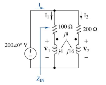
Find the phasor current \(I\) and the input impedance seen by the source in Figure P15-26. 200
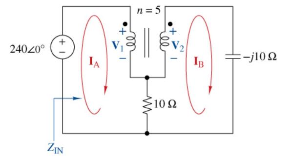
Find \(\mathbf{I}_{A}\) and \(\mathbf{I}_{\mathrm{B}}\) in Figure P15-27 and the input impedance seen by the voltage source. 24020 ZIN IA | el n=5 + ill
If \(f=50 \mathrm{~Hz}\), find \(\mathbf{V}_{1}\) and \(\mathbf{V}_{2}\) in Figure P15-27 using Multisim.
A transformer operating in the sinusoidal steady state has inductances \(L_{1}=800 \mathrm{mH}, L_{2}=320 \mathrm{mH}\), and \(M=500\) \(\mathrm{mH}\). A load \(Z_{\mathrm{L}}=6+j\) o \(\Omega\) is connected across the secondary. The \(60-\mathrm{Hz}\) voltage source connected to the primary side
A transformer operating in the sinusoidal steady state has inductances \(L_{1}=510 \mathrm{mH}, L_{2}=2 \mathrm{H}\), and \(M=1 \mathrm{H}\). The load connected across the secondary is \(Z_{\mathrm{L}}=200+j 150 \Omega\). The \(50-\) \(\mathrm{Hz}\) voltage source connected to the primary side has
The linear transformer in Figure \(\mathrm{P} 15=31\) is in the sinusoidal steady state with reactances of \(X_{1}=32 \Omega, X_{2}=50 \Omega\), \(X_{\mathrm{M}}=40 \Omega\), and a load impedance of \(Z_{\mathrm{L}}=150-j 50 \Omega\). Find the input impedance seen by the voltage source. Vs +1 ZIN -
An inductor \(L\) is connected across the secondary of an ideal transformer whose turns ratio is \(1: n\).(a) Derive an expression for the equivalent inductance \(L_{\mathrm{EQ}}\) seen looking into the primary winding.(b) Suppose you added a capacitor in parallel with the inductor. At what
A Transformer Thévenin Equivalent In the time domain, the \(i-v\) equations for a linear transformer are\[\begin{aligned}& v_{1}(t)=L_{1} \frac{d i_{1}(t)}{d t}+M \frac{d i_{2}(t)}{d t} \\& v_{2}(t)=M \frac{d i_{1}(t)}{d t}+L_{2} \frac{d i_{2}(t)}{d t}\end{aligned}\]Assuming zero initial
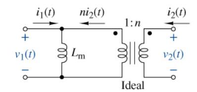
Figure P15:34 is an equivalent circuit of a perfectly coupled transformer. This model is the basis for the transformer equivalent circuits used in the analysis of power systems. The inductance \(L_{\mathrm{m}}\) is called the magnetizing inductance. The current through this inductance represents
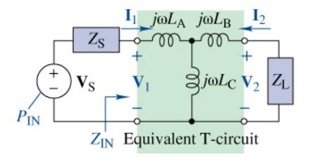
A Equivalent T-Circuit Transformer Model The transformer model shown in Figure 15-17 can also be modeled using an Equivalent T-Circuit as shown in Figure P15= 35 . The three inductors are related to the transformer inductances as follows:\[\begin{aligned}& L_{\mathrm{A}}=L_{1} \mp M \\&
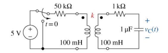
Consider the circuit shown in Figure P15-3 2 . The \(5-\mathrm{V}\) dc source switches from \(5 \mathrm{~V}\) to \(\mathrm{O}\) at \(t=0\). Find the output \(v_{\mathrm{C}}(t)\) for six different values of the coupling coefficient \(k(0,0.2,0.4,0.6\), 0.8 , and 0.999 ). Build your circuit in
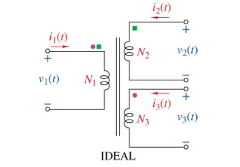
(a) Figure P15:37 shows a three-winding transformer that can be treated as ideal.Perfect coupling between all windings implies that \(v_{2}(t)=\frac{N_{2}}{N_{1}} v_{1}(t)\) and \(v_{3}(t)=\frac{N_{3}}{N_{1}} v_{1}(t)\).Show that zero power loss means that \(N_{1} i_{1}(t)+N_{2} i_{2}(t\) )
The following sets of \(v(t)\) and \(i(t)\) apply to the load circuit in Figure P16-1. Find the average power, reactive power, and instantaneous power delivered to the load.(a) \(v(t)=220 \cos \left(\omega t-60^{\circ}ight) \mathrm{V}, i(t)=200 \cos \left(\omega t+30^{\circ}ight)\)
The following sets of \(v(t)\) and \(i(t)\) apply to the load circuit in Figure P16-1. Calculate the average power, the reactive power, and instantaneous power delivered to the load.(a) \(v(t)=100 \cos \left(\omega t-15^{\circ}ight) \mathrm{V}, i(t)=100 \sin (\omega t) \mathrm{mA}\)(b) \(v(t)=1000
Showing 2700 - 2800
of 5433
First
21
22
23
24
25
26
27
28
29
30
31
32
33
34
35
Last
Step by Step Answers