New Semester
Started
Get
50% OFF
Study Help!
--h --m --s
Claim Now
Question Answers
Textbooks
Find textbooks, questions and answers
Oops, something went wrong!
Change your search query and then try again
S
Books
FREE
Study Help
Expert Questions
Accounting
General Management
Mathematics
Finance
Organizational Behaviour
Law
Physics
Operating System
Management Leadership
Sociology
Programming
Marketing
Database
Computer Network
Economics
Textbooks Solutions
Accounting
Managerial Accounting
Management Leadership
Cost Accounting
Statistics
Business Law
Corporate Finance
Finance
Economics
Auditing
Tutors
Online Tutors
Find a Tutor
Hire a Tutor
Become a Tutor
AI Tutor
AI Study Planner
NEW
Sell Books
Search
Search
Sign In
Register
study help
computer science
systems analysis design
The Analysis And Design Of Linear Circuits 10th Edition Roland E. Thomas, Albert J. Rosa, Gregory J. Toussaint - Solutions
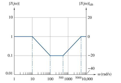
Consider the gain plot in Figure P12-53 .(a) Find a transfer function corresponding to the straight-line gain plot. Note that the magnitude of the actual frequency response must be exactly 5 at the geometric mean of the two cutoff frequencies ( \(245 \mathrm{rad} / \mathrm{s}\) ).(b) Use MATLAB to
Consider the gain plot in Figure P12-54.(a) Find the transfer function corresponding to the straightline gain plot.(b) Use MATLAB to plot the Bode magnitude of the transfer function.(c) Design a circuit that will realize the transfer function found in part (a).(d) Use Multisim to verify your
Consider the following transfer function:\[T_{\mathrm{V}}(s)=\frac{K}{s^{2}+B s+10^{10}}\](a) Select \(K\) so that the passband gain is \(+60 \mathrm{~dB}\).(b) Using MATLAB plot three different Bode magnitude plots on the same graph with \(\mathrm{B}=2000,20,000\), and 200,000. Bodemag (TT1, TT2,
The step response of a linear circuit is\[g(t)=50 e^{-5000 t} u(t)\](a) Find the impulse response waveform, \(h(t)\).(b) Is the circuit a low-pass, high-pass, bandpass, or bandstop filter?(c) Use MATLAB to plot the Bode magnitude and step responses.(d) Design a circuit to achieve the transfer
A circuit has the following transfer function:\[T(s)=\frac{s^{2}}{s^{2}+1500 s+2 \times 10^{6}}\](a) Use MATLAB to find its Bode magnitude response.(b) Use MATLAB to find its step response.(c) Determine the filter type, its cutoff frequency, and maximum gain.(d) Determine the circuit's \(\zeta\)
Select \(B\) in the following transfer function so that the step response is Case B (two equal roots).\[T_{\mathrm{V}}(s)=\frac{10^{7}}{s^{2}+B s+10^{8}}\]Verify your choice using MATLAB's step routine. Does this bandwidth result in the poles occurring at the value of \(\omega_{0}\) ? What is the
The following two transfer functions look similar. The difference is that their numerators and denominators are reversed. One is a tuned (narrow bandpass filter), the other is a notch (narrow bandstop) filter. Their frequency responses seem identical except for one being a notch and the other
There is a need for a passive notch filter at 10 \(\mathrm{krad} / \mathrm{s}\). The narrower the notch the better, but there should be minimal ringing of the signals passing through. The transforms of three filters were submitted for consideration. Which would you recommend and
There is a need for a filter to reduce the interference from a powerline on radio equipment. The interference is not only at \(60 \mathrm{~Hz}\) but also at its second harmonic, \(120 \mathrm{~Hz}\). Design a filter that is narrow, with a \(Q\) of 60 or better, and removes both frequencies but not
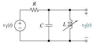
Step Response of an RLC Bandpass Circuit The step response of a series \(R L C\) bandpass circuit is\[g(t)=\left[\frac{4}{5} e^{-100 t} \sin (500 t)ight] u(t)\](a) Find the passband center frequency, the two cutoff frequencies, and the \(Q\) of the function.(b) Design a circuit that would possess
A Tunable Tank Circuit The RLC circuit in Figure P1263 (often called a tank circuit) has \(R=4.7 \mathrm{k} \Omega, C=68 \mathrm{opF}\), and an adjustable (tunable) \(L\) ranging from 64 to \(640 \mu \mathrm{H}\).(a) Show that the circuit is a bandpass filter.(b) Find the frequency range (in
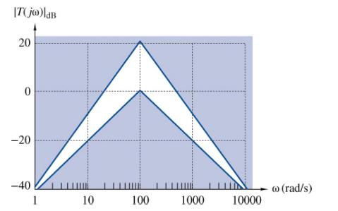
Filter Design Specification(a) Construct a transfer function whose gain response lies entirely within the nonshaded region in Figure P12-64. Validate your results using MATLAB.(b) If in addition to fitting in the shaded region the response must have the smallest overshoot possible, how would that
Networks Integrated circuit (chip) \(R C\) networks are used at parallel data ports to suppress radio frequency noise. In a certain application, RF noise at \(3.2 \mathrm{MHz}\) is interfering with a 4-bit parallel data signal operating at \(1.1 \mathrm{MHz}\). A chip \(R C\) network is to be used
Design Evaluation Your company issued a request for proposals listing the following design requirements and evaluation criteria.Design Requirements : Design a low-pass filter with a passband gain of \(9 \pm 10 \%\) and a cutoff frequency of \(90 \pm 10 \%\) \(\mathrm{krad} / \mathrm{s}\). A sensor
Design EvaluationIn a research laboratory, you need a bandpass filter to meet the following requirements:Design Requirements: Passband gain: \(10 \pm 5 \%, B=10 \mathrm{krad} / \mathrm{s} \pm\) \(5 \%, \omega_{\mathrm{O}}=5 \mathrm{krad} / \mathrm{s} \pm 2 \%, \omega_{\mathrm{CL}}=2 \mathrm{krad} /
Design EvaluationIn a cable service distribution station, you need a bandstop filter to meet the following requirements:Design Requirements: Passband gain: \(10 \pm 5 \%, B=3.3 \mathrm{kHz} \pm\) \(5 \%, f_{\mathrm{O}}=500 \mathrm{~Hz} \pm 2 \%, f_{\mathrm{CL}}=75 \mathrm{~Hz} \pm 10 \%\). Filter
The transfer function for a second-order LPF with \(T_{\max }=\mathrm{OdB}\) is\[T_{\mathrm{V}}(s)=\frac{\omega_{0}^{2}}{s^{2}+2 \zeta \omega_{0} s+\omega_{0}^{2}}\]Find the location of the poles that will cause the cutoff frequency \(\omega\) \({ }_{\mathrm{C}}\) to equal the resonant frequency
Determining the Cutoff Frequency of Two OnePole Filters in Cascade(a) Often one needs a simple cascaded low-pass \(R C\) filter that will achieve \(-40 \mathrm{~dB} / \mathrm{dec}\). Cascading two identical filters separated by a follower would seem to provide the answer. However, each filter will
Fiber-Optic Versus Cellular Communications Today, \(5 \mathrm{G}\) communications are necessary to deliver high band-widths and high-speed data to enable streaming of all types of information to control widely distributed items and processes. Recently, cellphone companies have obtained access to a
The OP AMP circuit in Figure P10-51 is in the zero state. Use node-voltage equations to find the circuit determinant. Select values of \(R, C_{1}\), and \(C_{2}\) so that the circuit has \(\omega_{0}=100 \mathrm{krad} / \mathrm{s}\) and \(\zeta=0.5\).
Assume that the circuits in Figures P10-50 and P10-51 both have the same response characteristics. What are the advantages and disadvantages of each?
The switch in Figure P10-53 has been in position A for a long time and is moved to position B at \(t=0\).(a) Write an appropriate set of node-voltage or mesh current equations in the \(s\) domain.(b) Use MATLAB to solve for \(V_{\mathrm{C}}(s)\) and \(v_{\mathrm{C}}(t)\) for \(V_{\mathrm{S}}(t\) )
There is no energy stored in the circuit in Figure P10-54 at \(t=0\). Transform the circuit into the \(s\) domain. Then use the unit output method to find the ratio \(V_{\mathrm{O}}(s) / V_{\mathrm{S}}(s)\). Subsequently, use the input \(v_{\mathrm{S}}(t)=100 u(t)\) and find the output
The switch in Figure P10-55 has been open for a long time and is closed at \(t=0\). Transform the circuit into the \(\mathrm{s}\) domain and solve for \(V_{\mathrm{O}}(s)\) and \(v_{\mathrm{O}}(t)\).
Show that the circuit in Figure P10-5 \(\underline{6}\) has natural poles at \(s=-4 / R C\) and \(s=-2 / R C \pm j 2 / R C\) when \(L=R^{2} C / 4\).
Find the range of the gain \(\mu\) for which the circuit's output \(V_{\mathrm{O}}(s)\) in Figure P10-57. is stable (i.e., all poles are in the lefthand side of the \(s\) plane.)
Consider what a pole-zero diagram can tell about the behavior of signals represented by their poles.(a) For example, consider a single pole, say \(V(s)=V_{\mathrm{A}} /(s\) \(+\alpha\) ). Let \(\alpha\) vary from a large negative number towards zero and then from zero to a large positive number.
The circuit in Figure P10-59. is shown in the \(t\) domain with initial values for the energy storage devices.(a) Transform the circuit into the \(s\) domain and write a set of node-voltage equations.(b) Transform the circuit into the \(s\) domain and write a set of mesh-current equations.(c) With
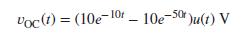
Thévenin's Theorem from Time-Domain Data A black box containing a linear circuit has an on-off switch and a pair of external terminals. When the switch is turned on, the open-circuit voltage between the external terminals is observed to beThe short-circuit current was observed to be(a) Locate the
In order to match the Thévenin impedance of a source, the load impedance in Figure P10-61 must be a equation(a) What impedance \(Z_{2}(s)\) is required if \(R=10 \Omega\) ?(b) How would you realize \(Z_{2}\) ( \(s\) ) using only resistors, inductors, and/or capacitors? ( Hint: Write
The \(R C\) circuits in Figure P10-62 represent the situation at the input to an oscilloscope. The parallel combination of \(R_{1}\) and \(C_{1}\) represents the probe used to connect the oscilloscope to a test point. The parallel combination of \(R_{2}\) and \(C_{2}\) represents the input
The OP AMP circuit in Figure P10-63 is in the zero state.(a) Transform the circuit into the \(s\) domain and use the \(\mathrm{OP}\) AMP circuit analysis techniques developed in Section 4-4 to find the network function \(V_{2}(s) / V_{1}(s)\).(b) Determine the possible purpose of this circuit by
The purpose of the test setup in Figure P10-64 is to deliver damped sine pulses to the test load. The excitation comes from a 1 -Hz square wave generator. The pulse conversion circuit must deliver damped sine waveforms with \(\zeta10 \mathrm{krad} / \mathrm{s}\) to \(50-\Omega\) and \(600-\Omega\)
In transistor amplifier design, a by-pass capacitor is connected across the emitter resistor \(R_{\mathrm{E}}\) to effectively short out the emitter resistor at signal frequencies. This design improves the gain of the transistor for the desired ac signals. The circuit in Figure P10-65 (a) is a
The Acme Pole Eliminator company states in their online catalog that the circuit shown in Figure P10-66 can eliminate any realizable pole. Their catalog states "Suppose you have a need to eliminate the pole associated with an input, for example, \(V_{\mathrm{S}}(s)=K /(s+\alpha)\). Selecting \(1 /
The OP AMP circuit in Figure P10-67 is an audio band-pass filter-amplifier.(a) Your task is to design such a filter so that the lowfrequency cutoff is \(80 \mathrm{~Hz}\) and the high-frequency cutoff is 25,000 Hz. The gain of the combined OP AMPs should be 1000. (b) Show that your design is
(a) Find the driving point impedance seen by the voltage source in Figure P11-1 and the voltage transfer function \(T_{\mathbf{V}}(s)=V_{\mathbf{2}}(s) / V_{1}(s)\).(b) Select values of \(R\) and \(C\) so that the transfer function has a zero at \(-1 \mathrm{krad} / \mathrm{s}\) and a pole at
(a) Find the driving point impedance seen by the voltage source in Figure P11-2 and the voltage transfer function \(T_{\mathrm{V}}(s)=V_{2}(s) / V_{1}(s)\).(b) Select values of \(R\) and \(L\) so that the transfer function has a zero at \(\mathrm{s}=-150 \mathrm{rad} / \mathrm{s}\) and a pole at
(a) Find the driving point impedance seen by the voltage source in Figure P11-3 and the voltage transfer function \(T_{\mathbf{V}}(s)=V_{\mathbf{2}}(s) / V_{1}(s)\).(b) Select values of \(R, L\), and \(C\) so that the transfer function has a pair of real poles at \(s=-10000 \mathrm{rad} /
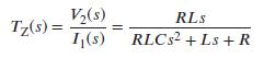
The transfer impedance function \(T_{\mathrm{Z}}(s)\) for the parallel circuit in Figure P11-4 isShow that the poles of the driving point impedance Z(s) are the poles of the transfer impedance function. Tz(s)= V(s) I(s) RLS RLCS2 + Ls +R
(a) Find the driving point impedance seen by the voltage source in Figure P11-5 and the voltage transfer function \(T_{\mathrm{V}}(s)=V_{\mathbf{2}}(s) / V_{1}(s)\).(b) Select values for \(R_{1}, R_{2}\), and \(C\) so that there is a pole in the transfer function at \(\mathrm{s}=-2000 \mathrm{rad}
(a) Find the driving point impedance seen by the voltage source in Figure P11-6 and the voltage transfer function \(T_{\mathrm{V}}(s)=V_{\mathbf{2}}(s) / V_{\mathbf{1}}(s)\).(b) Select values for \(R_{1}, R_{2}, C_{1}\), and \(C_{2}\) so that there is a pole in the transfer function at
(a) Find the voltage transfer function \(T_{\mathrm{V}}(s)=V_{2}(s\))/ \(V_{1}(s)\) in Figure P11-7.(b) With \(L=1 \mathrm{H}\), select values of \(C\) and \(R\) so that poles are located at \(-2000 \pm j 2000 \mathrm{rad} / \mathrm{s}\). Is the circuit stable?
(a) Find the driving point impedance seen by the voltage source in Figure P11-8 and the voltage transfer function \(T_{\mathrm{V}}\) \((s)=V_{2}(s) / V_{1}(s)\).(b) Insert a follower at A and repeat. What effect on the location of the poles did the follower have?
(a) Find the driving point impedance seen by \(V_{1}(s)\) in Figure P11-9.(b) Find the voltage transfer function \(T_{\mathrm{V}}(s)=V_{2}(s) / V_{1}\) ( \(s\) ).(c) Select values of \(R_{1}, R_{2}, \mu\), and \(C\) so that \(T_{\mathrm{V}}(s)\) has a pole at \(s=-500 \mathrm{krad} /
(a) Do a source transformation for \(I_{1}(s)\) and \(R\).(b) Use the new Thévenin source to find the transfer function \(T_{\mathrm{Z}}(s)=V_{2}(s) / I_{1}(s)\).(c) Select values of \(R\) and \(L\) so that there is a pole at -3000 \(\mathrm{rad} / \mathrm{s}\). Where is the zero?
Find the voltage transfer function \(T_{\mathrm{V}}(s)=V_{2}(\) \(s) / V_{1}(s)\) of the cascade connection in Figure P11-11. Locate the poles and zeros of the transfer function.
The circuit of Figure P11-12 consists of two stages - a voltage divider stage and an OP AMP stage.(a) Compute the transfer function \(T_{\mathrm{V}_{1}}(s)=V_{\mathrm{X}}(s) / V_{1}(\) \(s)\).(b) Compute the transfer function \(T_{\mathrm{V} 2}(s)=V_{2}(s) / V_{\mathrm{X}}(\) \(s)\).(c) Compute the
For the circuit in Figure P11-13 :(a) Find the impulse response \(h_{2}(t)\).(b) Find the step response \(g_{2}(t)\).
Find \(v_{2}(t)\) in Figure P11-14 when \(v_{1}(t)=\delta(t)\). Repeat for \(v_{1}(t)=u(t)\).
(a) Find \(h(t)\) and \(g(t)\) for the circuit in Figure P11-15 .(b) Swap the inductor and capacitor in the shaded portion of the circuit and repeat (a).
(a) Find \(H(s)\) for the circuit in Figure P11-16 in terms of \(R_{\mathrm{F}}\).(b) Select a value of \(R_{\mathrm{F}}\) so that there is pole in \(H\) ( \(s\) )at \(s=\) \(-5000 \mathrm{rad} / \mathrm{s}\).(c) With the \(R_{\mathrm{F}}\) you found, find \(h(t)\) by hand.(d) Use the step function
If \(R_{\mathrm{F}}\) in Figure \(\mathrm{P}_{11-16}\) is \(25 \mathrm{k} \Omega\), find \(G(s)\) and \(g\) \((t)\). What are the initial value and final value of the step response?
Find \(v_{2}(t)\) in Figure P11-18 when \(v_{1}(t)=\delta(t)\). Repeat for \(v_{1}(t)=u(t)\).
The impulse response of a linear circuit is \(h(t)\) \(=\delta(t)-500 e^{-100 t} u(t)\). Find the circuit's step response \(g(t)\), impulse response transform \(H(s)\), step response transform \(G(\) \(s\) ), and the circuit's transfer function \(T(s)\).
The step response transform of a linear circuit is \(G(s)=200 / s(s+100)\).(a) Find the circuit's transfer function, \(T(s)\).(b) Design a circuit to produce that transfer function. ( Hint : See Design Exercise 11-26 .)(c) Find the circuit's impulse response \(h(t)\) and step response \(g(t)\).(d)
The pole-zero diagram of a circuit's step response is shown in Figure P11-21. The \(K\) of the circuit is 500.(a) Find \(G(s), g(t), H(s), T(s)\), and \(h(t)\).(b) Design an \(R C\) circuit that can realize the step response.
Find \(h(t)=\) image when \(g(t)=\left(3-e^{-10 t}ight) u(t)\). Verify your answer by first transforming \(g(t)\) into \(G(s)\) and finding \(H(s)=s G(s)\) and then taking the inverse transform of \(H(s)\). Did you get the same answer?
The impulse response of a linear circuit is \(h(t)\) \(=45,000\left[e^{-5000 t}ight] u(t)\). Find the output waveform when the input is \(x(t)=9 t u(t) \mathrm{V}\).
The step response of a linear circuit is \(g(t)=0.5\) [1\(\left.e^{-250 t}ight] u(t)\). Find the output waveform when the input is \(v_{1}(\) \(t)=\left[20 e^{-200 t}ight] u(t)\). Use MATLAB to find the Laplace transforms of \(g(t)\) and \(v_{1}(t)\). Then find \(V_{2}(s)\). Finally, use the
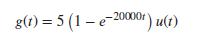
(a) Design a circuit that has the following step response:(b) Validate your design using Multisim(c) Plot its pole-zero diagram What is its scaling factor \(K\) ? or) u(t) 8(1) = 5(1-e-20000r)
The step response of a linear circuit is \(g(t)=100\left[\mathrm{e}^{-100}ight.\) \(\left.{ }^{t} \cos 2000 tight] u(t)\). Find the circuit's impulse response \(h(t)\), impulse response transform \(H(s)\), step response transform \(G(\) \(s\) ), and the circuit's transfer function \(T(s)\).
The transfer function of a linear circuit is \(T\) ( \(s)=(s+2000) /(s+1000)\). Find the output waveform when the input is \(x(t)=5 e^{-1000 t} u(t)\). Use MATLAB to find the Laplace transform of \(x(t)\). Then find \(Y(s)\). Finally, use the inverse Laplace function to find the waveform \(y(t)\)
The circuit in Figure P11-28 is in the steady state with \(v_{1}\) \((t)=10 \cos 1414.21 t \mathrm{~V}\). Find \(v_{2 S S}(t)\). Repeat for \(v_{1}(t)=10\) \(\cos 10 \mathrm{k} t \mathrm{~V}\). And without doing any calculations, repeat for \(v_{1}(t\) )\(=10 \mathrm{~V}\).
The circuit in Figure P11-29. is in the steady state with \(v_{1}(t)=1.0 \cos 2020 t \mathrm{~V}\). Find \(v_{2 S S}(t)\). Repeat for \(v\) \({ }_{1}(t)=1.0 \cos 20.2 \mathrm{k} t \mathrm{~V}\), and for \(v_{1}(t)=1.0 \cos 202 \mathrm{k} t \mathrm{~V}\). Where is the pole located?
The output in Figure P11-30 is \(v_{2 S S}(t)=25.5 \cos\) \(\left(10,000 t+11.8^{\circ}ight) \mathrm{V}\). Find the input \(v_{1}(t)\) that produced that output.
The circuit in Figure P11-31 is in the steady state with \(i_{1}(t)=100 \cos (25 \mathrm{k} t) \mathrm{mA}, R_{1}=4 \mathrm{k} \Omega, R_{2}=6 \mathrm{k} \Omega\), and \(L\) \(=500 \mathrm{mH}\).(a) Find \(i_{2 S S}(t)\).(b) Find the location of the pole by running an ac sweep on Multisim. Run your
The circuit in Figure P11-32 is in the steady state.(a) If \(i_{1}(t)=10 \cos 500 t \mathrm{~mA}\), find \(v_{2 S S}(t)\)(b) If \(i_{1}(t)=10 \cos 5000 t \mathrm{~mA}\), find \(v_{2 S S}(t)\).(c) If \(i_{1}(t)=10 \cos 50,000 t \mathrm{~mA}\), find \(v_{2 S S}(t)\).(d) Verify your results using
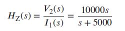
The impulse response transform of a circuit is(a) Find \(v_{1 \mathrm{SS}}(t)\) if \(i_{1}(t)=10 \cos 5000 t \mathrm{~mA}\).(b) Design a circuit to achieve \(H_{Z}(s)\). The circuit in Figure P11-32 must be part of your design. Hz(s) = V(s) I(s) 10000S s + 5000
The transfer function of a linear circuit is \(T(s)=(s\) \(+100) /(s+200\). Find the sinusoidal steady-state output for an input \(x(t)=15 \cos 200 t\).
The step response of a linear circuit is \(g(t)\) \(=\left[5 e^{-1000 t}ight] u(t)\). Find the sinusoidal steady-state output for an input \(x(t)=10 \cos 1000 t\).
A student looks back at some notes she took in class. She sees Figure P11-3 6 and an equation \(v_{2}(t)=(1-\) \(\left.e^{-2 \text { equation }}ight) u(t)\) after it. How are the figure and the equation related, if at all?
The impulse response of a linear circuit is \(h(t)=800\left[e^{-100 t}-\mathrm{e}^{-400 t}ight] u(t)\). Use MATLAB to find the sinusoidal steady-state output for an input \(x(t)=\) \(8 \cos 200 t\). Use MATLAB to plot \(y(t)\).
The step response of a linear circuit is \(g(t)=\left[2 e^{-}ight.\) \(\left.{ }^{50 t} \sin 200 tight] u(t)\). Find the sinusoidal steady-state response for an input \(x(t)=50 \cos 200 t\).
The step response of a linear circuit is \(g(t)\) \(=\left[1-10ight.\) te \(\left.e^{-10 t}ight] u(t)\). The sinusoidal steady-state response is noted to be \(y_{\mathrm{SS}}(t)=18.03 \cos \left(20 t+19.4^{\circ}ight)\). What was the input that caused that output?
The impulse response of a linear circuit is \(h(t)=u\) \((t)\). Use the convolution integral to find the response due to an input \(x(t)=\delta(t)\).
The impulse response of a linear circuit is \(h\) ( \(t)=[3 u(t)-u(t-1)-2 u(t-2)]\). Use the convolution integral to find the response due to an input \(x(t)=\delta(t)\).
The impulse response of a linear circuit is \(h(t)=u(\) \(t)-u(t-2)\). Use the convolution integral to find the response due to an input \(x(t)=u(t)-u(t-1)\).
The impulse response of a linear circuit is \(h\) \((t)=t[u(t)-u(t-1)]\). Use the convolution integral to find the response due to an input \(x(t)=u(t-2)\).
(a) The impulse response of a linear circuit is \(h\) ( \(t\) )\(=e^{-2 t} u(t)\). Use the convolution integral to find the response due to an input \(x(t)=\delta(t)\). Repeat for \(x(t)\) \(=u(t)\).(b) Convert the impulse response into a transfer function and the input into the \(s\) domain. Solve
(a) The impulse response of a linear circuit is \(h(t)=e\) \({ }^{-2 t} u(t)\). Use the convolution integral to find the response due to an input \(x(t)=t u(t)\).(b) Convert the impulse response into a transfer function and the input into the \(s\) domain. Solve the problem in the \(s\) domain and
Show that \(f(t) * \delta(t)=f(t)\). That is, show that convolving any waveform \(f(t)\) with an impulse leaves the waveform unchanged.
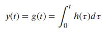
Use the convolution integral to show that if the input to a linear circuit is \(x(t)=u(t)\), thenThat is, show that the step response is the integral of the impulse response. y(t) = g(t) = S 0 h(t)dt
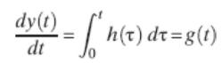
If the input to a linear circuit is \(x(t)=t u(t)\), then the output \(y(t)\) is called the ramp response. Use the convolution integral to show thatThat is, show that the derivative of the ramp response is the step response. dy(t) dt = [ "h(r) dr = g(1)
The impulse response of a linear circuit is \(h(t)=t u(t)\). Use MATLAB to compute the convolution integral and find the response due to an input \(x(t)=t[u(\) \(t)-u(t-2)]\).
The step response of a linear circuit is \(g(t)=2(1-\) \(\left.e^{-50 t}ight) u(t)\) and \(x(t)=' t u(t)\) Use \(s\)-domain convolution to find the zero-state response \(y(t)\)
The impulse responses of two linear circuits are \(h_{1}(t)=5 e^{-5 t} u(t)\) and \(h_{2}(t)=15 e^{-3 t} u(t)\) What is the impulse response of a cascade connection of these two circuits?
The impulse response of a linear circuit is shown in Figure P11-52. Graphically find the convolution of the impulse response shown and a unit step function, \(x(t)=u\) \((t)\).
Solve Problem 11–40 graphically.
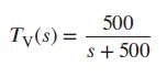
Design an \(R C\) circuit using practical values to realize the following transfer function: Ty(s) = 500 s + 500
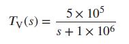
Design an \(R L\) circuit using practical values to realize the following transfer function: Ty(s) = 5 x 10⁵ s+1x 10⁶
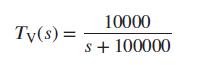
Design a circuit to realize the transfer function below \(\pm 2 \%\) using only resistors and capacitors, but no OP AMPs, since no external power is available. You must use those \(100 \mathrm{pF}\) capacitors that are surplus. Be sure to minimize loading. Ty(s) = 10000 s+100000
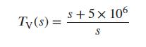
Design a circuit to realize the transfer function below using only resistors, inductors, and no more than one OP AMP.Scale the circuit so that all inductors are exactly \(10 \mathrm{mH}\). Ty(s) = S+5x10⁶ S
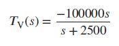
Design a circuit to realize the transfer function below using only resistors, capacitors, and OP AMPs. All \(R\) s must be 1 \(\mathrm{k} \Omega\). or larger and the maximum OP AMP gain is \(\pm 10^{4}\).Scale the circuit so that all capacitors are exactly \(0.1 \mu \mathrm{F}\). Ty(s) = -100000s S
The circuit shown in Figure P11-59. was designed to produce the following transfer function
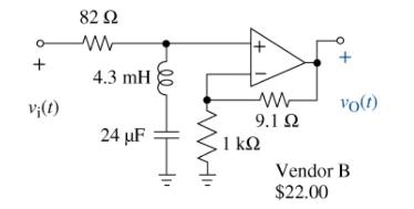
Your employer needs a circuit that meets specific criteria. It must meet the following transfer characteristics:All capacitors must be exactly \(0.1 \mu \mathrm{F}\) and resistors greater than 1 \(\mathrm{k} \Omega\). You contact a manufacturer who claims that the circuit shown in Figure P11-60 can
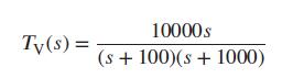
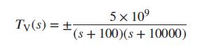
Design a circuit to realize the transfer function below using only resistors, capacitors, and OP AMPs. Scale the circuit so that all resistors are greater than \(10 \mathrm{k} \Omega\) and all capacitors are less the \(1 \mu \mathrm{F}\). 5 x 10 (s + 100)(s + 10000) Ty(s) =
Design a circuit to realize the following transfer function image in two ways:(a) As a passive circuit using only resistors, capacitors, and inductors with \(L \leq 50 \mathrm{mH}\).(b) Using only one OP AMP and identical resistors and capacitors. Must use \(C=0.033 \mu \mathrm{F}\).
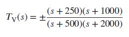
A circuit is needed to realize the transfer function listed below.(a) Design the circuit using two OP AMPs.(b) Design the circuit using only one OP AMP.(c) Design the circuit using no OP AMPs. (s +250) (s +1000) Ty(s) = (s +500)(s+2000)
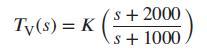
It is claimed that both circuits in Figure P11-64. realize the transfer function(a) Verify that both circuits realize the specified \(T_{\mathrm{v}}(s)\).(b) Which circuit would you choose if the output must drive a \(1 \mathrm{k} \Omega\) load?(c) Which circuit would you choose if the input comes
Showing 3100 - 3200
of 5433
First
25
26
27
28
29
30
31
32
33
34
35
36
37
38
39
Last
Step by Step Answers