New Semester
Started
Get
50% OFF
Study Help!
--h --m --s
Claim Now
Question Answers
Textbooks
Find textbooks, questions and answers
Oops, something went wrong!
Change your search query and then try again
S
Books
FREE
Study Help
Expert Questions
Accounting
General Management
Mathematics
Finance
Organizational Behaviour
Law
Physics
Operating System
Management Leadership
Sociology
Programming
Marketing
Database
Computer Network
Economics
Textbooks Solutions
Accounting
Managerial Accounting
Management Leadership
Cost Accounting
Statistics
Business Law
Corporate Finance
Finance
Economics
Auditing
Tutors
Online Tutors
Find a Tutor
Hire a Tutor
Become a Tutor
AI Tutor
AI Study Planner
NEW
Sell Books
Search
Search
Sign In
Register
study help
computer science
systems analysis and design 12th
Microelectronics Circuit Analysis And Design 4th Edition Donald A. Neamen - Solutions
Sketch a simple source-follower amplifier circuit and discuss the general ac circuit characteristics (voltage gain and output resistance).
Sketch a simple common-gate amplifier circuit and discuss the general ac circuit characteristics (voltage gain and output resistance).
Discuss the general conditions under which a source-follower or a common-gate amplifier would be used.
Compare the ac circuit characteristics of the common-source, source-follower, and common-gate circuits.
State the advantage of using transistors in place of resistors in MOSFET integrated circuits.
State at least two reasons why a multistage amplifier circuit would be required in a design compared to using a single-stage circuit.
An NMOS transistor has parameters \(V_{T N}=0.4 \mathrm{~V}, k_{n}^{\prime}=100 \mu \mathrm{A} / \mathrm{V}^{2}\), and \(\lambda=0.02 \mathrm{~V}^{-1}\).(a) (i) Determine the width-to-length ratio \(W / L\) such that \(g_{m}=0.5 \mathrm{~mA} / \mathrm{V}\) at \(I_{D Q}=0.5 \mathrm{~mA}\) when
A PMOS transistor has parameters \(V_{T P}=-0.6 \mathrm{~V}, k_{p}^{\prime}=40 \mu \mathrm{A} / \mathrm{V}^{2}\), and \(\lambda=0.015 \mathrm{~V}^{-1}\).(a) (i) Determine the width-to-length ratio \((W / L)\) such that \(g_{m}=1.2 \mathrm{~mA} / \mathrm{V}\) at \(I_{D Q}=0.15 \mathrm{~mA}\). (ii)
An NMOS transistor is biased in the saturation region at a constant \(V_{G S}\). The drain current is \(I_{D}=3 \mathrm{~mA}\) at \(V_{D S}=5 \mathrm{~V}\) and \(I_{D}=3.4 \mathrm{~mA}\) at \(V_{D S}=\) \(10 \mathrm{~V}\). Determine \(\lambda\) and \(r_{o}\).
The minimum value of small-signal resistance of a PMOS transistor is to be \(r_{o}=100 \mathrm{k} \Omega\). If \(\lambda=0.012 \mathrm{~V}^{-1}\), calculate the maximum allowed value of \(I_{D}\).
An n-channel MOSFET is biased in the saturation region at a constant \(V_{G S}\). (a) The drain current is \(I_{D}=0.250 \mathrm{~mA}\) at \(V_{D S}=1.5 \mathrm{~V}\) and \(I_{D}=0.258 \mathrm{~mA}\) at \(V_{D S}=3.3 \mathrm{~V}\). Determine the value of \(\lambda\) and \(r_{o}\). (b) Using the
The value of \(\lambda\) for a MOSFET is \(0.02 \mathrm{~V}^{-1}\). (a) What is the value of \(r_{o}\) at (i) \(I_{D}=50 \mu \mathrm{A}\) and at (ii) \(I_{D}=500 \mu \mathrm{A}\) ? (b) If \(V_{D S}\) increases by \(1 \mathrm{~V}\), what is the percentage increase in \(I_{D}\) for the conditions
A MOSFET with \(\lambda=0.01 \mathrm{~V}^{-1}\) is biased in the saturation region at \(I_{D}=\) \(0.5 \mathrm{~mA}\). If \(V_{G S}\) and \(V_{D S}\) remain constant, what are the new values of \(I_{D}\) and \(r_{o}\) if the channel length \(L\) is doubled?
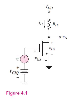
The parameters of the circuit in Figure 4.1 are \(V_{D D}=3.3 \mathrm{~V}\) and \(R_{D}=5 \mathrm{k} \Omega\). The transistor parameters are \(k_{n}^{\prime}=100 \mu \mathrm{A} / \mathrm{V}^{2}, W / L=40\), \(V_{T N}=0.4 \mathrm{~V}\), and \(\lambda=0.025 \mathrm{~V}^{-1}\). (a) Find \(I_{D Q}\)
The circuit shown in Figure 4.1 has parameters \(V_{D D}=2.5 \mathrm{~V}\) and \(R_{D}=10 \mathrm{k} \Omega\). The transistor is biased at \(I_{D Q}=0.12 \mathrm{~mA}\). The transistor parameters are \(V_{T N}=0.3 \mathrm{~V}, k_{n}^{\prime}=100 \mu \mathrm{A} / \mathrm{V}^{2}\), and
For the circuit shown in Figure 4.1, the transistor parameters are \(V_{T N}=0.6 \mathrm{~V}, k_{n}^{\prime}=80 \mu \mathrm{A} / \mathrm{V}^{2}\), and \(\lambda=0.015 \mathrm{~V}^{-1}\). Let \(V_{D D}=5 \mathrm{~V}\). (a) Design the transistor width-to-length ratio \(W / L\) and the resistance
In our analyses, we assumed the small-signal condition given by Equation (4.4). Now consider Equation (4.3(b)) and let \(v_{g s}=V_{g s} \sin \omega t\). Show that the ratio of the signal at frequency \(2 \omega\) to the signal at frequency \(\omega\) is given by \(V_{g S} /\left[4\left(V_{G
Using the results of Problem 4.11, find the peak amplitude \(V_{g s}\) that produces a second-harmonic distortion of 1 percent if \(V_{G S}=3 \mathrm{~V}\) and \(V_{T N}=1 \mathrm{~V}\).Data From Problem 4.11:-In our analyses, we assumed the small-signal condition given by Equation (4.4). Now
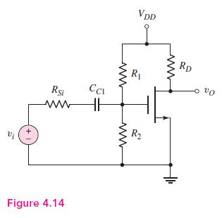
Consider the circuit in Figure 4.14 in the text. The circuit parameters are \(V_{D D}=3.3 \mathrm{~V}, R_{D}=8 \mathrm{k} \Omega, R_{1}=240 \mathrm{k} \Omega, R_{2}=60 \mathrm{k} \Omega\), and \(R_{S i}=2 \mathrm{k} \Omega\). The transistor parameters are \(V_{T N}=0.4 \mathrm{~V},
A common-source amplifier, such as shown in Figure 4.14 in the text, has parameters \(r_{o}=100 \mathrm{k} \Omega\) and \(R_{D}=5 \mathrm{k} \Omega\). Determine the transconductance of the transistor if the small-signal voltage gain is \(A_{v}=-10\). Assume \(R_{S i}=0\). Vi VDD www R Rsi CCI www
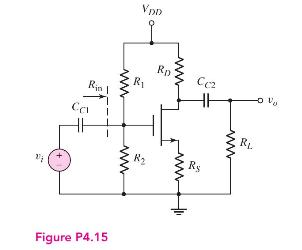
For the NMOS common-source amplifier in Figure P4.15, the transistor parameters are: \(V_{T N}=0.8 \mathrm{~V}, K_{n}=1 \mathrm{~mA} / \mathrm{V}^{2}\), and \(\lambda=0\). The circuit parameters are \(V_{D D}=5 \mathrm{~V}, R_{S}=1 \mathrm{k} \Omega, R_{D}=4 \mathrm{k} \Omega, R_{1}=225 \mathrm{k}
The parameters of the circuit shown in Figure P4.15 are \(V_{D D}=12 \mathrm{~V}\), \(R_{S}=0.5 \mathrm{k} \Omega, R_{i n}=250 \mathrm{k} \Omega\), and \(R_{L}=10 \mathrm{k} \Omega\). The transistor parameters are \(V_{T N}=1.2 \mathrm{~V}, K_{n}=1.5 \mathrm{~mA} / \mathrm{V}^{2}\), and
Repeat Problem 4.15 if the source resistor is bypassed by a source capacitor \(C_{S}\).Data From Problem 4.15:-For the NMOS common-source amplifier in Figure P4.15, the transistor parameters are: \(V_{T N}=0.8 \mathrm{~V}, K_{n}=1 \mathrm{~mA} / \mathrm{V}^{2}\), and \(\lambda=0\). The circuit
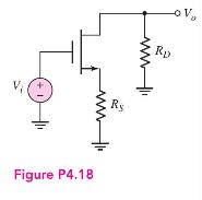
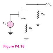
The ac equivalent circuit of a common-source amplifier is shown in Figure P4.18. The small-signal parameters of the transistor are \(g_{m}=2 \mathrm{~mA} / \mathrm{V}\) and \(r_{o}=\infty\). (a) The voltage gain is found to be \(A_{v}=V_{o} / V_{i}=-15\) with \(R_{S}=0\). What is the value of
Consider the ac equivalent circuit shown in Figure P4.18. Assume \(r_{o}=\infty\) for the transistor. The small-signal voltage gain is \(A_{v}=-8\) for the case when \(R_{S}=1 \mathrm{k} \Omega\). (a) When \(R_{S}\) is shorted \(\left(R_{S}=0\right)\), the magnitude of the voltage gain doubles.
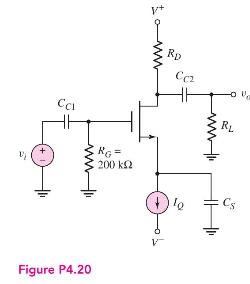
The transistor in the common-source amplifier in Figure P4.20 has parameters \(V_{T N}=0.8 \mathrm{~V}, k_{n}^{\prime}=100 \mu \mathrm{A} / \mathrm{V}^{2}, W / L=50\), and \(\lambda=0.02 \mathrm{~V}^{-1}\). The circuit parameters are \(V^{+}=5 \mathrm{~V}, V^{-}=-5 \mathrm{~V}, I_{Q}=0.5
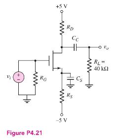
The parameters of the MOSFET in the circuit shown in Figure P4.21 are \(V_{T N}=0.8 \mathrm{~V}, K_{n}=0.85 \mathrm{~mA} / \mathrm{V}^{2}\), and \(\lambda=0.02 \mathrm{~V}^{-1}\). (a) Determine \(R_{S}\) and \(R_{D}\) such that \(I_{D Q}=0.1 \mathrm{~mA}\) and \(V_{D S Q}=5.5 \mathrm{~V}\). (b)
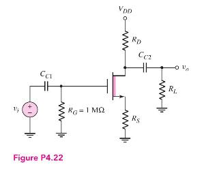
For the common-source amplifier in Figure P4.22, the transistor parameters are \(V_{T N}=-0.8 \mathrm{~V}, K_{n}=2 \mathrm{~mA} / \mathrm{V}^{2}\), and \(\lambda=0\). The circuit parameters are \(V_{D D}=3.3 \mathrm{~V}\) and \(R_{L}=10 \mathrm{k} \Omega\). (a) Design the circuit such that \(I_{D
The transistor in the common-source circuit in Figure P4.22 has the same parameters as given in Problem 4.22. The circuit parameters are \(V_{D D}=5 \mathrm{~V}\) and \(R_{D}=R_{L}=2 \mathrm{k} \Omega\). (a) Find \(R_{S}\) for \(V_{D S Q}=2.5 \mathrm{~V}\). (b) Determine the small-signal voltage
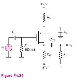
Consider the PMOS common-source circuit in Figure P4.24 with transistor parameters \(V_{T P}=-2 \mathrm{~V}\) and \(\lambda=0\), and circuit parameters \(R_{D}=R_{L}=\) \(10 \mathrm{k} \Omega\).(a) Determine the values of \(K_{p}\) and \(R_{S}\) such that \(V_{S D Q}=6 \mathrm{~V}\).(b) Determine
For the common-source circuit in Figure P4.24, the bias voltages are changed to \(V^{+}=3 \mathrm{~V}\) and \(V^{-}=-3 \mathrm{~V}\). The PMOS transistor parameters are: \(V_{T P}=-0.5 \mathrm{~V}, K_{p}=0.8 \mathrm{~mA} / \mathrm{V}^{2}\), and \(\lambda=0\). The load resistor is \(R_{L}=\) \(2
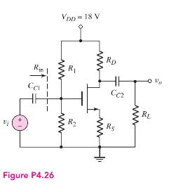
Design the common-source circuit in Figure P4.26 using an n-channel MOSFET with \(\lambda=0\). The quiescent values are to be \(I_{D Q}=6 \mathrm{~mA}\), \(V_{G S Q}=2.8 \mathrm{~V}\), and \(V_{D S Q}=10 \mathrm{~V}\). The transconductance is \(g_{m}=2.2 \mathrm{~mA} / \mathrm{V}\). Let \(R_{L}=1
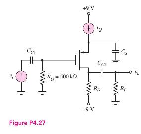
For the common-source amplifier shown in Figure P4.27, the transistor parameters are \(V_{T P}=-1.2 \mathrm{~V}, K_{p}=2 \mathrm{~mA} / \mathrm{V}^{2}\), and \(\lambda=0.03 \mathrm{~V}^{-1}\). The drain resistor is \(R_{D}=4 \mathrm{k} \Omega\).(a) Determine \(I_{Q}\) such that \(V_{S D Q}=5
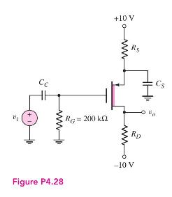
For the circuit shown in Figure P4.28, the transistor parameters are: \(V_{T P}=0.8 \mathrm{~V}, K_{p}=0.25 \mathrm{~mA} / \mathrm{V}^{2}\), and \(\lambda=0\). (a) Design the circuit such that \(I_{D Q}=0.5 \mathrm{~mA}\) and \(V_{S D Q}=3 \mathrm{~V}\). (b) Determine the small-signal voltage gain
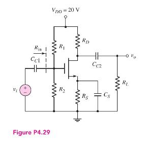
Design a common-source amplifier, such as that in Figure P4.29, to achieve a small-signal voltage gain of at least \(A_{v}=v_{o} / v_{i}=-10\) for \(R_{L}=20 \mathrm{k} \Omega\) and \(R_{\text {in }}=200 \mathrm{k} \Omega\). Assume the \(Q\)-point is chosen at \(I_{D Q}=1 \mathrm{~mA}\) and \(V_{D
The small-signal parameters of an enhancement-mode MOSFET source follower are \(g_{m}=5 \mathrm{~mA} / \mathrm{V}\) and \(r_{o}=100 \mathrm{k} \Omega\). (a) Determine the no-load small-signal voltage gain and the output resistance. (b) Find the smallsignal voltage gain when a load resistance
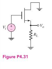
The open-circuit \(\left(R_{L}=\infty\right)\) voltage gain of the ac equivalent sourcefollower circuit shown in Figure P4.31 is \(A_{v}=0.98\). When \(R_{L}\) is set to \(1 \mathrm{k} \Omega\), the voltage gain is reduced to \(A_{v}=0.49\). What are the values of \(g_{m}\) and \(r_{o}\) ? + RI.
Consider the source-follower circuit in Figure P4.31. The small-signal parameters of the transistor are \(g_{m}=2 \mathrm{~mA} / \mathrm{V}\) and \(r_{o}=25 \mathrm{k} \Omega\). (a) Determine the open-circuit \(\left(R_{L}=\infty\right)\) voltage gain and output resistance. (b) If \(R_{L}=2
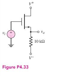
The source follower amplifier in Figure P4.33 is biased at \(V^{+}=1.5 \mathrm{~V}\) and \(V^{-}=-1.5 \mathrm{~V}\). The transistor parameters are \(V_{T N}=0.4 \mathrm{~V}\), \(k_{n}^{\prime}=100 \mu \mathrm{A} / \mathrm{V}^{2}, W / L=80\), and \(\lambda=0.02 \mathrm{~V}^{-1}\). (a) The dc value
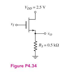
Consider the circuit in Figure P4.34. The transistor parameters are \(V_{T N}=0.6 \mathrm{~V}, k_{n}^{\prime}=100 \mu \mathrm{A} / \mathrm{V}^{2}\), and \(\lambda=0\). The circuit is to be designed such that \(V_{D S Q}=1.25 \mathrm{~V}\) and such that the small-signal voltage gain is
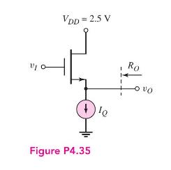
The quiescent power dissipation in the circuit in Figure P4.35 is to be limited to \(2.5 \mathrm{~mW}\). The parameters of the transistor are \(V_{T N}=0.6 \mathrm{~V}\), \(k_{n}^{\prime}=100 \mu \mathrm{A} / \mathrm{V}^{2}\), and \(\lambda=0.02 \mathrm{~V}^{-1}\).(a) Determine \(I_{Q}\).(b)
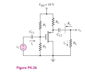
The parameters of the circuit in Figure P4.36 are \(R_{S}=4 \mathrm{k} \Omega, R_{1}=850 \mathrm{k} \Omega\), \(R_{2}=350 \mathrm{k} \Omega\), and \(R_{L}=4 \mathrm{k} \Omega\). The transistor parameters are \(V_{T P}=-1.2 \mathrm{~V}\), \(k_{p}^{\prime}=40 \mu \mathrm{A} / \mathrm{V}^{2}, W /
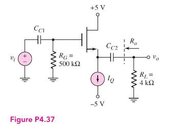
Consider the source follower circuit in Figure P4.37 with transistor parameters \(V_{T N}=0.8 \mathrm{~V}, k_{n}^{\prime}=100 \mu \mathrm{A} / \mathrm{V}^{2}, W / L=20\), and \(\lambda=0.02 \mathrm{~V}^{-1}\).(a) Let \(I_{Q}=5 \mathrm{~mA}\). (i) Determine the small-signal voltage gain. (ii) Find
For the source-follower circuit shown in Figure P4.37, the transistor parameters are: \(V_{T N}=1 \mathrm{~V}, k_{n}^{\prime}=60 \mu \mathrm{A} / \mathrm{V}^{2}\), and \(\lambda=0\). The small-signal voltage gain is to be \(A_{v}=v_{o} / v_{i}=0.95\). (a) Determine the required width-to-length
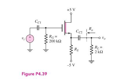
In the source-follower circuit in Figure P4.39 with a depletion NMOS transistor, the device parameters are: \(V_{T N}=-2 \mathrm{~V}, K_{n}=5 \mathrm{~mA} / \mathrm{V}^{2}\), and \(\lambda=0.01 \mathrm{~V}^{-1}\). Design the circuit such that \(I_{D Q}=5 \mathrm{~mA}\). Find the smallsignal voltage
For the circuit in Figure P4.39, \(R_{S}=1 \mathrm{k} \Omega\) and the quiescent drain current is \(I_{D Q}=5 \mathrm{~mA}\). The transistor parameters are \(V_{T N}=-2 \mathrm{~V}\), \(k_{n}^{\prime}=100 \mu \mathrm{A} / \mathrm{V}^{2}\), and \(\lambda=0.01 \mathrm{~V}^{-1}\). (a) Determine the
For the source-follower circuit in Figure P4.39, the transistor parameters are: \(V_{T N}=-2 \mathrm{~V}, K_{n}=4 \mathrm{~mA} / \mathrm{V}^{2}\), and \(\lambda=0\). Design the circuit such that \(R_{o} \leq 200 \Omega\). Determine the resulting small-signal voltage gain. +5 V CCI RG= 200 R CC2 w
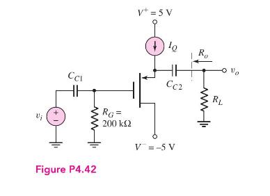
The current source in the source-follower circuit in Figure P4.42 is \(I_{Q}=10 \mathrm{~mA}\) and the transistor parameters are \(V_{T P}=-2 \mathrm{~V}, K_{p}=5 \mathrm{~mA} / \mathrm{V}^{2}\), and \(\lambda=0.01 \mathrm{~V}^{-1}\). (a) Find the open circuit \(\left(R_{L}=\infty\right)\)
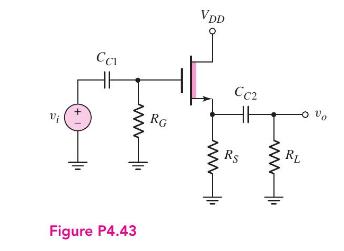
Consider the source-follower circuit shown in Figure P4.43. The most negative output signal voltage occurs when the transistor just cuts off. Show that this output voltage \(v_{o}(\mathrm{~min})\) is given by\(v_{o}(\min )=\frac{-I_{D Q} R_{S}}{1+\frac{R_{S}}{R_{L}}}\)Show that the corresponding
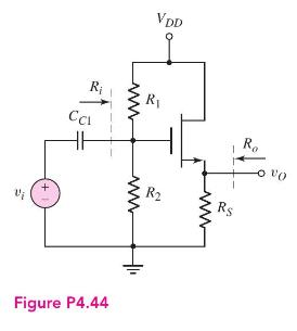
The transistor in the circuit in Figure P4.44 has parameters \(V_{T N}=0.4 \mathrm{~V}\), \(K_{n}=0.5 \mathrm{~mA} / \mathrm{V}^{2}\), and \(\lambda=0\). The circuit parameters are \(V_{D D}=3 \mathrm{~V}\) and \(R_{i}=300 \mathrm{k} \Omega\). (a) Design the circuit such that \(I_{D Q}=0.25
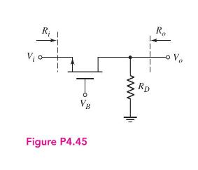
Figure P4.45 is the ac equivalent circuit of a common-gate amplifier. The transistor parameters are \(V_{T N}=0.4 \mathrm{~V}, k_{n}^{\prime}=100 \mu \mathrm{A} / \mathrm{V}^{2}\), and \(\lambda=0\). The quiescent drain current is \(I_{D Q}=0.25 \mathrm{~mA}\). Determine the transistor \(W / L\)
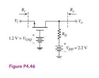
The transistor in the common-gate circuit in Figure P4.46 has the same parameters that are given in Problem 4.45. The output resistance \(R_{o}\) is tobe \(500 \Omega\) and the drain-to-source quiescent voltage is to be \(V_{D S Q}=V_{D S}(\) sat \()+0.3 \mathrm{~V}\). (a) What is the value of
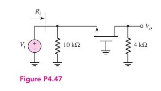
The small-signal parameters of the NMOS transistor in the ac equivalent common-gate circuit shown in Figure P4.47 are \(V_{T N}=0.4 \mathrm{~V}, k_{n}^{\prime}=100 \mu \mathrm{A} / \mathrm{V}^{2}\), \(W / L=80\), and \(\lambda=0\). The quiescent drain current is \(I_{D Q}=0.5 \mathrm{~mA}\).
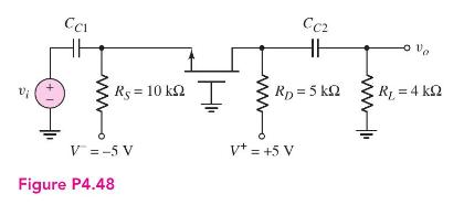
For the common-gate circuit in Figure P4.48, the NMOS transistor parameters are: \(V_{T N}=1 \mathrm{~V}, K_{n}=3 \mathrm{~mA} / \mathrm{V}^{2}\), and \(\lambda=0\). (a) Determine \(I_{D Q}\) and \(V_{D S Q}\). (b) Calculate \(g_{m}\) and \(r_{o}\). (c) Find the small-signal voltage gain
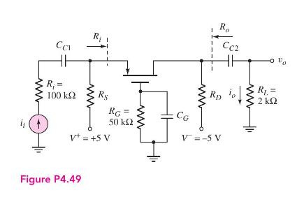
Consider the PMOS common-gate circuit in Figure P4.49. The transistor parameters are: \(V_{T P}=-1 \mathrm{~V}, K_{p}=0.5 \mathrm{~mA} / \mathrm{V}^{2}\), and \(\lambda=0\). (a) Determine \(R_{S}\) and \(R_{D}\) such that \(I_{D Q}=0.75 \mathrm{~mA}\) and \(V_{S D Q}=6 \mathrm{~V}\). (b) Determine
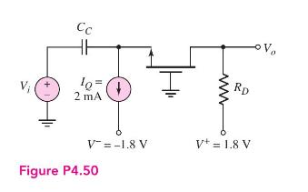
The transistor parameters of the NMOS device in the common-gate amplifier in Figure P4.50 are \(V_{T N}=0.4 \mathrm{~V}, k_{n}^{\prime}=100 \mu \mathrm{A} / \mathrm{V}^{2}\), and \(\lambda=0\). (a) Find \(R_{D}\) such that \(V_{D S Q}=V_{D S}\) (sat) \(+0.25 \mathrm{~V}\). (b) Determine the
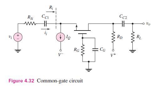
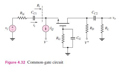
The parameters of the circuit shown in Figure 4.32 are \(V^{+}=3.3 \mathrm{~V}\), \(V^{-}=-3.3 \mathrm{~V}, R_{G}=50 \mathrm{k} \Omega, R_{L}=4 \mathrm{k} \Omega, R_{\mathrm{Si}}=0\), and \(I_{Q}=2 \mathrm{~mA}\). The transistor parameters are \(V_{T N}=0.6 \mathrm{~V}, K_{n}=4 \mathrm{~mA} /
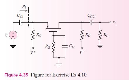
For the common-gate amplifier in Figure 4.35 in the text, the PMOS transistor parameters are \(V_{T P}=-0.8 \mathrm{~V}, K_{p}=2.5 \mathrm{~mA} / \mathrm{V}^{2}\), and \(\lambda=0\). The circuit parameters are \(V^{+}=3.3 \mathrm{~V}, V^{-}=-3.3, R_{G}=100 \mathrm{k} \Omega\), and \(R_{L}=4
Consider the NMOS amplifier with saturated load in Figure 4.39(a). The transistor parameters are \(V_{T N D}=V_{T N L}=0.6 \mathrm{~V}, k_{n}^{\prime}=100 \mu \mathrm{A} / \mathrm{V}^{2}, \lambda=0\), and \((W / L)_{L}=1\). Let \(V_{D D}=3.3 \mathrm{~V}\). (a) Design the circuit such that the
For the NMOS amplifier with depletion load in Figure 4.43(a), the transistor parameters are \(V_{T N D}=0.6 \mathrm{~V}, V_{T N L}=-0.8 \mathrm{~V}, K_{n D}=1.2 \mathrm{~mA} / \mathrm{V}^{2}\), \(K_{n L}=0.2 \mathrm{~mA} / \mathrm{V}^{2}\), and \(\lambda_{D}=\lambda_{L}=0.02 \mathrm{~V}^{-1}\). Let
Consider a saturated load device in which the gate and drain of an enhancement-mode MOSFET are connected together. The transistor drain current becomes zero when \(V_{D S}=0.6 \mathrm{~V}\). (a) At \(V_{D S}=1.5 \mathrm{~V}\), the drain current is \(0.5 \mathrm{~mA}\). Determine the small-signal
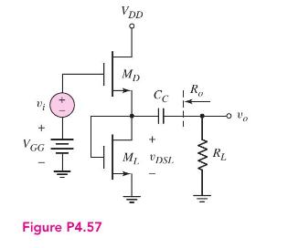
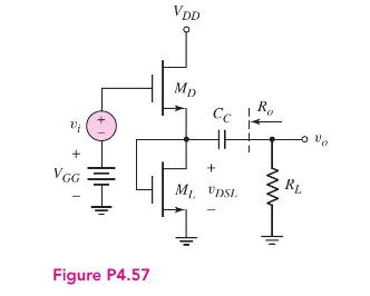
A source-follower circuit with a saturated load is shown in Figure P4.57. The transistor parameters are \(V_{T N D}=1 \mathrm{~V}, K_{n D}=1 \mathrm{~mA} / \mathrm{V}^{2}\) for \(M_{D}\), and \(V_{T N L}=1 \mathrm{~V}, K_{n L}=0.1 \mathrm{~mA} / \mathrm{V}^{2}\) for \(M_{L}\). Assume \(\lambda=0\)
For the source-follower circuit with a saturated load as shown in Figure P4.57, assume the same transistor parameters as given in Problem 4.57. (a) Determine the small-signal voltage gain if \(R_{L}=10 \mathrm{k} \Omega\). (b) Determine the small-signal output resistance \(R_{o}\). Vi VGG Figure
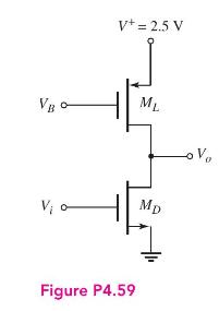
The transistor parameters for the common-source circuit in Figure P4.59 are \(V_{T N D}=0.4 \mathrm{~V}, \quad V_{T P L}=-0.4 \mathrm{~V}, \quad(W / L)_{L}=50, \quad \lambda_{D}=0.02 \mathrm{~V}^{-1}\), \(\lambda_{L}=0.04 \mathrm{~V}^{-1}, k_{n}^{\prime}=100 \mu \mathrm{A} / \mathrm{V}^{2}\), and
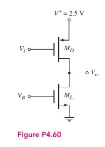
Consider the circuit in Figure P4.60. The transistor parameters are \(V_{T P D}=-0.6 \mathrm{~V}, \quad V_{T N L}=0.4 \mathrm{~V}, \quad k_{n}^{\prime}=100 \mu \mathrm{A} / \mathrm{V}^{2}, \quad k_{p}^{\prime}=40 \mu \mathrm{A} / \mathrm{V}^{2}\), \(\lambda_{L}=0.02 \mathrm{~V}^{-1},
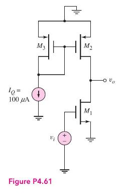
The ac equivalent circuit of a CMOS common-source amplifier is shown in Figure P4.61. The transistor parameters for \(M_{1}\) are \(V_{T N}=0.5 \mathrm{~V}, k_{n}^{\prime}=\) \(85 \mu \mathrm{A} / \mathrm{V}^{2},(W / L)_{1}=50\), and \(\lambda=0.05 \mathrm{~V}^{-1}\), and for \(M_{2}\) and
Consider the ac equivalent circuit of a CMOS common-source amplifier shown in Figure P4.62. The parameters of the NMOS and PMOS transistors are the same as given in Problem 4.61. Determine the small-signal voltage gain.Data From Problem 4.61:-The ac equivalent circuit of a CMOS common-source
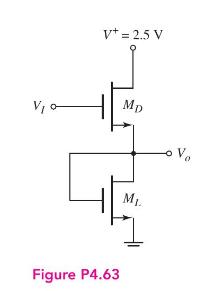
The parameters of the transistors in the circuit in Figure \(\mathrm{P} 4.63\) are \(V_{T N D}=\) \(V_{T N L}=0.4 \mathrm{~V}, K_{n D}=2 \mathrm{~mA} / \mathrm{V}^{2}, K_{n L}=0.5 \mathrm{~mA} / \mathrm{V}^{2}\), and \(\lambda_{D}=\lambda_{L}=0\). (a) Plot \(V_{o}\) versus \(V_{I}\) over the range
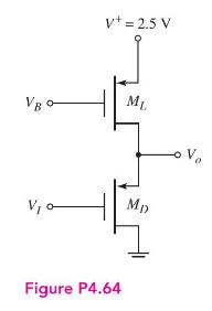
Consider the source-follower circuit in Figure P4.64. The transistor parameters are \(V_{T P}=-0.4 \mathrm{~V}, k_{p}^{\prime}=40 \mu \mathrm{A} / \mathrm{V}^{2},(W / L)_{L}=5,(W / L)_{D}=50\), and \(\lambda_{D}=\lambda_{L}=0.025 \mathrm{~V}^{-1}\). Assume \(V_{B}=1 \mathrm{~V}\).(a) What is the
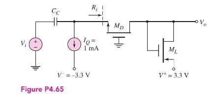
Figure P4.65 shows a common-gate amplifier. The transistor parameters are \(V_{T N}=0.6 \mathrm{~V}, V_{T P}=-0.6 \mathrm{~V}, K_{n}=2 \mathrm{~mA} / \mathrm{V}^{2}, K_{p}=0.5 \mathrm{~mA} / \mathrm{V}^{2}\), and \(\lambda_{n}=\lambda_{p}=0\). (a) Find the values of \(V_{S G L Q}, V_{G S D Q}\),
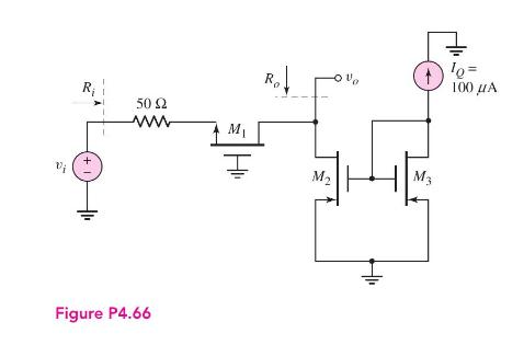
The ac equivalent circuit of a CMOS common-gate circuit is shown in Figure P4.66. The parameters of the NMOS and PMOS transistors are the same as given in Problem 4.61. Determine the (a) small-signal parameters of the transistors, (b) small-signal voltage gain \(A_{v}=v_{o} / v_{i}\), (c) input
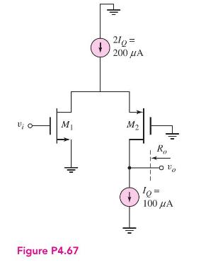
The circuit in Figure P4.67 is a simplified ac equivalent circuit of a foldedcascode amplifier. The transistor parameters are \(\left|V_{T N}\right|=\left|V_{T P}\right|=0.5 \mathrm{~V}\), \(K_{n}=K_{p}=2 \mathrm{~mA} / \mathrm{V}^{2}\), and \(\lambda_{n}=\lambda_{p}=0.1 \mathrm{~V}^{-1}\). Assume
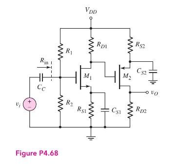
The transistor parameters in the circuit in Figure P4.68 are \(V_{T N 1}=0.6 \mathrm{~V}\), \(V_{T P 2}=-0.6 \mathrm{~V}, K_{n 1}=0.2 \mathrm{~mA} / \mathrm{V}^{2}, K_{p 2}=1.0 \mathrm{~mA} / \mathrm{V}^{2}\), and \(\lambda_{1}=\lambda_{2}=0\). The circuit parameters are \(V_{D D}=5 \mathrm{~V}\)
The transistor parameters in the circuit in Figure P4.68 are the same as those given in Problem 4.68. The circuit parameters are \(V_{D D}=3.3 \mathrm{~V}\), \(R_{S 1}=1 \mathrm{k} \Omega\), and \(R_{\mathrm{in}}=250 \mathrm{k} \Omega\). (a) Design the circuit such that \(I_{D Q 1}=0.1
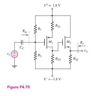
Consider the circuit shown in Figure P4.70. The transistor parameters are \(V_{T P 1}=-0.4 \mathrm{~V}, \quad V_{T N 2}=0.4 \mathrm{~V}, \quad(W / L)_{1}=20, \quad(W / L)_{2}=80\), \(k_{p}^{\prime}=40 \mu \mathrm{A} / \mathrm{V}^{2}, k_{n}^{\prime}=100 \mu \mathrm{A} / \mathrm{V}^{2}\), and
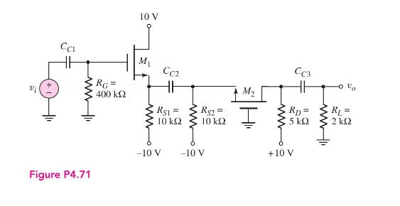
For the circuit in Figure P4.71, the transistor parameters are: \(K_{n 1}=\) \(K_{n 2}=4 \mathrm{~mA} / \mathrm{V}^{2}, V_{T N 1}=V_{T N 2}=2 \mathrm{~V}\), and \(\lambda_{1}=\lambda_{2}=0\). (a) Determine \(I_{D Q 1}, I_{D Q 2}, V_{D S Q 1}\), and \(V_{D S Q 2}\). (b) Determine \(g_{m 1}\) and
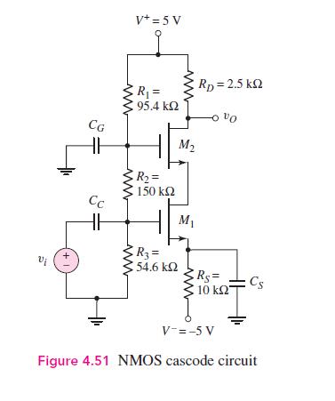
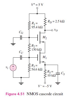
For the cascode circuit in Figure 4.51 in the text, the transistor parameters are: \(V_{T N 1}=V_{T N 2}=1 \mathrm{~V}, K_{n 1}=K_{n 2}=2 \mathrm{~mA} / \mathrm{V}^{2}\), and \(\lambda_{1}=\lambda_{2}=0\). (a) Let \(R_{S}=1.2 \mathrm{k} \Omega\) and \(R_{1}+R_{2}+R_{3}=500 \mathrm{k} \Omega\).
The supply voltages to the cascode circuit in Figure 4.51 in the text are changed to \(V^{+}=10 \mathrm{~V}\) and \(V^{-}=-10 \mathrm{~V}\). The transistor parameters are: \(K_{n 1}=K_{n 2}=4 \mathrm{~mA} / \mathrm{V}^{2}, V_{T N 1}=V_{T N 2}=1.5 \mathrm{~V}\), and \(\lambda_{1}=\lambda_{2}=0\).
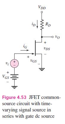
Consider the JFET amplifier in Figure 4.53 with transistor parameters \(I_{D S S}=6 \mathrm{~mA}, V_{P}=-3 \mathrm{~V}\), and \(\lambda=0.01 \mathrm{~V}^{-1}\). Let \(V_{D D}=10 \mathrm{~V}\). (a) Determine \(R_{D}\) and \(V_{G S}\) such that \(I_{D Q}=4 \mathrm{~mA}\) and \(V_{D S Q}=6
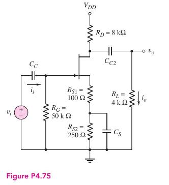
For the JFET amplifier in Figure P4.75, the transistor parameters are: \(I_{D S S}=2 \mathrm{~mA}, V_{P}=-2 \mathrm{~V}\), and \(\lambda=0\). Determine \(g_{m}, A_{v}=v_{o} / v_{i}\), and \(A_{i}=i_{o} / i_{i}\). Cc Figure P4.75 VDD ww RD=8 k2 HH CC2 - Vo R$1 = 100 RG= 50 Rs2= 250 ww www R = Cs
The parameters of the transistor in the JFET common-source amplifier shown in Figure P4.76 are: \(I_{D S S}=8 \mathrm{~mA}, V_{P}=-4.2 \mathrm{~V}\), and \(\lambda=0\). Let \(V_{D D}=20 \mathrm{~V}\) and \(R_{L}=16 \mathrm{k} \Omega\). Design the circuit such that \(V_{S}=2 \mathrm{~V}\),
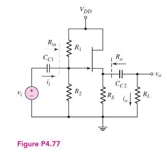
Consider the source-follower JFET amplifier in Figure P4.77 with transistor parameters \(I_{D S S}=10 \mathrm{~mA}, V_{P}=-5 \mathrm{~V}\), and \(\lambda=0.01 \mathrm{~V}^{-1}\). Let \(V_{D D}=12 \mathrm{~V}\) and \(R_{L}=0.5 \mathrm{k} \Omega\). (a) Design the circuit such that \(R_{\text {in
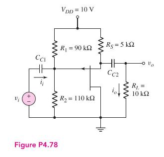
For the p-channel JFET source-follower circuit in Figure P4.78, the transistor parameters are: \(I_{D S S}=2 \mathrm{~mA}, V_{P}=+1.75 \mathrm{~V}\), and \(\lambda=0\). (a) Determine \(I_{D Q}\) and \(V_{S D Q}\). (b) Determine the small-signal gains \(A_{v}=v_{o} / v_{i}\) and \(A_{i}=\) \(i_{o} /
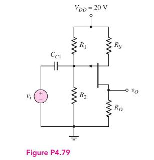
The p-channel JFET common-source amplifier in Figure P4.79 has transistor parameters \(I_{D S S}=8 \mathrm{~mA}, V_{P}=4 \mathrm{~V}\), and \(\lambda=0\). Design the circuit such that \(I_{D Q}=4 \mathrm{~mA}, V_{S D Q}=7.5 \mathrm{~V}, A_{v}=v_{o} / v_{i}=-3\), and \(R_{1}+R_{2}=\) \(400
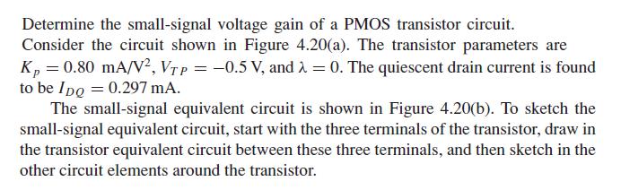
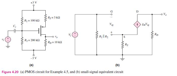
Consider the common-source circuit described in Example 4.5. (a) Using a computer simulation, verify the results obtained in Example 4.5. (b) Determine the change in the results when the body effect is taken into account.Data From Example 4.5:- Determine the small-signal voltage gain of a PMOS
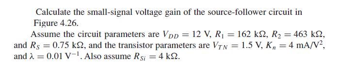
Using a computer simulation, verify the results of Example 4.7 for the source-follower amplifier.Data From Example 4.7:- Calculate the small-signal voltage gain of the source-follower circuit in Figure 4.26. Assume the circuit parameters are VDD = 12 V, R = 162 ks, R = 463 ks, and Rs = 0.75 ks2,
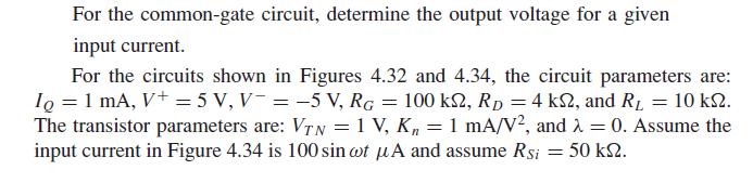
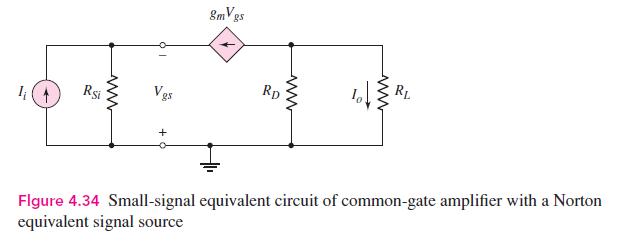
Using a computer simulation, verify the results of Example 4.10 for the common-gate amplifier.Data From Example 4.10:- For the common-gate circuit, determine the output voltage for a given input current. For the circuits shown in Figures 4.32 and 4.34, the circuit parameters are: I = 1 mA, V+ = 5
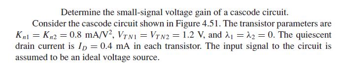
Using a computer simulation, verify the results of Example 4.17 for the cascode amplifier.Data From Example 4.17:- Determine the small-signal voltage gain of a cascode circuit. Consider the cascode circuit shown in Figure 4.51. The transistor parameters are Kn1 = Kn2 = 0.8 mA/V2, VTN = VTN2 = 1.2
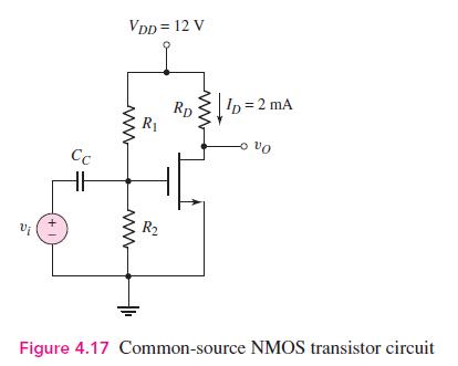
A discrete common-source circuit with the configuration shown in Figure 4.17 is to be designed to provide a voltage gain of 18 and a symmetrical output voltage swing. The bias voltage is \(V_{D D}=3.3 \mathrm{~V}\), the output resistance of the signal source is \(500 \Omega\), and the transistor
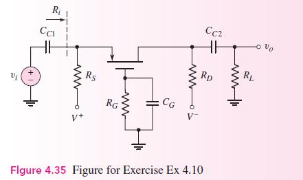
Consider the common-gate amplifier shown in Figure 4.35. The power supply voltages are \(\pm 5 \mathrm{~V}\), the output resistance of the signal source is \(500 \Omega\), and the input resistance of the amplifier is to be \(200 \Omega\). The transistor parameters are \(k_{p}^{\prime}=40 \mu
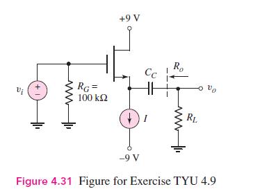
A source-follower amplifier with the configuration shown in Figure 4.31 is to be designed. The power supplies are to be \(\pm 12 \mathrm{~V}\). The transistor parameters are \(V_{T N}=1.2 \mathrm{~V}, k_{n}^{\prime}=100 \mu \mathrm{A} / \mathrm{V}^{2}\), and \(\lambda=0\). The load resistance is
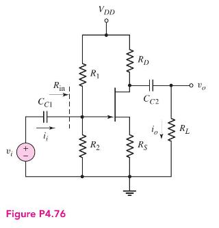
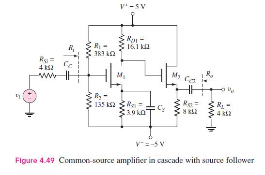
Consider the multitransistor circuit in Figure 4.49. Assume transistor parameters of \(V_{T N}=0.6 \mathrm{~V}, k_{n}^{\prime}=100 \mu \mathrm{A} / \mathrm{V}^{2}\), and \(\lambda=0\). Design the transistors such that the small-signal voltage gain of the first stage is \(A_{v 1}=-10\) and the
Describe an intrinsic semiconductor material. What is meant by the intrinsic carrier concentration?
Describe the concept of an electron and a hole as charge carriers in the semiconductor material.
Describe an extrinsic semiconductor material. What is the electron concentration in terms of the donor impurity concentration? What is the hole concentration in terms of the acceptor impurity concentration?
Describe the concepts of drift current and diffusion current in a semiconductor material.
How is a pn junction formed? What is meant by a built-in potential barrier, and how is it formed?
How is a junction capacitance created in a reverse-biased pn junction diode?
Write the ideal diode current-voltage relationship. Describe the meaning of \(I_{S}\) and \(V_{T}\).
Describe the iteration method of analysis and when it must be used to analyze a diode circuit.
Showing 1400 - 1500
of 4723
First
8
9
10
11
12
13
14
15
16
17
18
19
20
21
22
Last
Step by Step Answers