New Semester
Started
Get
50% OFF
Study Help!
--h --m --s
Claim Now
Question Answers
Textbooks
Find textbooks, questions and answers
Oops, something went wrong!
Change your search query and then try again
S
Books
FREE
Study Help
Expert Questions
Accounting
General Management
Mathematics
Finance
Organizational Behaviour
Law
Physics
Operating System
Management Leadership
Sociology
Programming
Marketing
Database
Computer Network
Economics
Textbooks Solutions
Accounting
Managerial Accounting
Management Leadership
Cost Accounting
Statistics
Business Law
Corporate Finance
Finance
Economics
Auditing
Tutors
Online Tutors
Find a Tutor
Hire a Tutor
Become a Tutor
AI Tutor
AI Study Planner
NEW
Sell Books
Search
Search
Sign In
Register
study help
computer science
systems analysis and design 12th
Microelectronics Circuit Analysis And Design 4th Edition Donald A. Neamen - Solutions
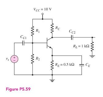
Design a bias-stable circuit in the form of Figure P5.59 with \(\beta=120\) such that \(I_{C Q}=0.8 \mathrm{~mA}, V_{C E Q}=5 \mathrm{~V}\), and the voltage across \(R_{E}\) is approximately \(0.7 \mathrm{~V}\). 1's 1+ Figure P5.59 Vcc = 10 V CCI R RC ww RE=0.5 kQ Cc2 HH R = 1
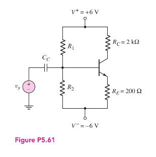
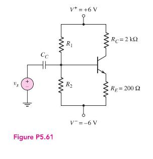
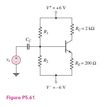
Using the circuit in Figure P5.61, design a bias-stable amplifier such that the \(Q\)-point is in the center of the load line. Let \(\beta=125\). Determine \(I_{C Q}\), \(V_{C E Q}, R_{1}\), and \(R_{2}\). Cc Figure P5.61 ww www V+=+6 V Rc=2 k R R RE=200 2 V-=-6 V
For the circuit shown in Figure P5.61, the bias voltages are changed to \(V^{+}=3 \mathrm{~V}\) and \(V^{-}=-3 \mathrm{~V}\).(a) Design a bias-stable circuit for \(\beta=120\) such that \(V_{C E Q}=2.8 \mathrm{~V}\). Determine \(I_{C Q}, R_{1}\), and \(R_{2}\).(b) If the resistors \(R_{1}\) and
(a) A bias-stable circuit with the configuration shown in Figure P5.61 is to be designed such that \(I_{C Q}=(3 \pm 0.1) \mathrm{mA}\) and \(V_{C E Q} \cong 5 \mathrm{~V}\) using a transistor with \(75 \leq \beta \leq 150\). (b) Sketch the load line and plot the range of \(Q\)-point values for part
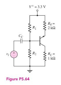
(a) For the circuit shown in Figure P5.64, assume that the transistor current gain is \(\beta=90\) and that the circuit parameter is \(R_{T H}=2.4 \mathrm{k} \Omega\). Design the circuit such that \(V_{E C Q}=1.5 \mathrm{~V}\). Find \(I_{B Q}, I_{C Q}, R_{1}\), and \(R_{2}\). (b) Determine the
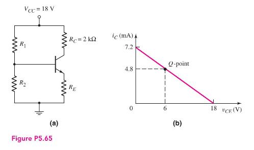
The dc load line and \(Q\)-point of the circuit in Figure P5.65 (a) are shown in Figure P5.65(b). For the transistor, \(\beta=120\). Find \(R_{E}, R_{1}\), and \(R_{2}\) such that the circuit is bias stable. ww www Vcc = 18 V Figure P5.65 (a) Rc=2 k ic (mA) RE 7.2 Q-point 4.8 0 18 "CE (V) (b)
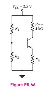
The range of \(\beta\) for the transistor in the circuit in Figure P5.66 is \(80 \leq \beta \leq 120\). Design a bias-stable circuit such that the nominal \(Q\)-point values are \(I_{C Q}=0.2 \mathrm{~mA}\) and \(V_{C E Q}=1.6 \mathrm{~V}\). The value of \(I_{C Q}\) must fall in the range \(0.19
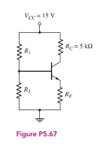
The nominal \(Q\)-point of the circuit in Figure P5.67 is \(I_{C Q}=1 \mathrm{~mA}\) and \(V_{C E Q}=5 \mathrm{~V}\), for \(\beta=60\). The current gain of the transistor is in the range \(45 \leq \beta \leq 75\). Design a bias-stable circuit such that \(I_{C Q}\) does not vary by more than 5
(a) For the circuit in Figure P5.67, the value of \(V_{C C}\) is changed to \(3 \mathrm{~V}\). Let \(R_{C}=5 R_{E}\) and \(\beta=120\). Redesign a bias-stable circuit such that \(I_{C Q}=\) \(100 \mu \mathrm{A}\) and \(V_{C E Q}=1.4 \mathrm{~V}\). (b) Using the results of part (a), determine the dc
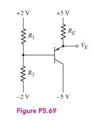
For the circuit in Figure P5.69, let \(\beta=100\) and \(R_{E}=3 \mathrm{k} \Omega\). Design a biasstable circuit such that \(V_{E}=0\). +2 V +5 V ww R RE R2 -2 V -5 V Figure P5.69 VE
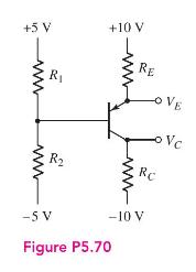
For the circuit in Figure P5.70, let \(R_{C}=2.2 \mathrm{k} \Omega, R_{E}=2 \mathrm{k} \Omega, R_{1}=10 \mathrm{k} \Omega\), \(R_{2}=20 \mathrm{k} \Omega\), and \(\beta=60\). (a) Find \(R_{T H}\) and \(V_{T H}\) for the base circuit. (b) Determine \(I_{B Q}, I_{C Q}, V_{E}\), and \(V_{C}\). +5 V
Design the circuit in Figure P5.70 to be bias stable and to provide nominal \(Q\)-point values of \(I_{C Q}=0.5 \mathrm{~mA}\) and \(V_{E C Q}=8 \mathrm{~V}\). Let \(\beta=60\). The maximum current in \(R_{1}\) and \(R_{2}\) is to be limited to \(40 \mu \mathrm{A}\). +5 V +10 V RE OVE o Vc RC -5 V
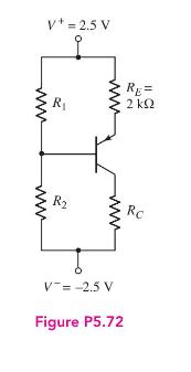
Consider the circuit shown in Figure P5.72. (a) The nominal transistor current gain is \(\beta=80\). Design a bias-stable circuit such that \(I_{C Q}=0.15 \mathrm{~mA}\) and \(V_{E C Q}=2.7 \mathrm{~V}\). (b) Using the results of part (a), determine the percent change in \(I_{C Q}\) and \(V_{E C
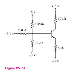
For the circuit in Figure P5.73, let \(\beta=100\). (a) Find \(V_{T H}\) and \(R_{T H}\) for the base circuit. (b) Determine \(I_{C Q}\) and \(V_{C E Q}\). +5 V +15 V 500 +3 Vo-ww 500 50 Figure P5.73 -5 V 70 -5 V 5
Design a bias-stable four-resistor bias network for an npn transistor such that \(I_{C Q}=0.8 \mathrm{~mA}, V_{C E Q}=4 \mathrm{~V}\), and \(V_{E}=1.5 \mathrm{~V}\). The circuit and transistor parameters are \(V_{C C}=10 \mathrm{~V}\) and \(\beta=120\), respectively.
(a) Design a four-resistor bias network with the configuration shown in Figure P5.61 to yield \(Q\)-point values of \(I_{C Q}=50 \mu \mathrm{A}\) and \(V_{C E Q}=5 \mathrm{~V}\). The bias voltages are \(V^{+}=+5 \mathrm{~V}\) and \(V^{-}=-5 \mathrm{~V}\). Assume a transistor with \(\beta=80\) is
(a) Design a four-resistor bias network with the configuration shown in Figure P5.61 to yield \(Q\)-point values of \(I_{C Q}=0.50 \mathrm{~mA}\) and \(V_{C E Q}=2.5 \mathrm{~V}\). The bias voltages are \(V^{+}=3 \mathrm{~V}\) and \(V^{-}=-3 \mathrm{~V}\). The transistor current gain is
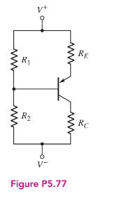
(a) A four-resistor bias network is to be designed with the configuration shown in Figure P5.77. The \(Q\)-point values are to be \(I_{C Q}=100 \mu \mathrm{A}\) and \(V_{E C Q}=3 \mathrm{~V}\). The bias voltages are \(V^{+}=3 \mathrm{~V}\) and \(V^{-}=-3 \mathrm{~V}\). A transistor with
(a) Design a four-resistor bias network with the configuration shown in Figure P5.77 such that the \(Q\)-point values are \(I_{C Q}=1.2 \mathrm{~mA}\) and \(V_{E C Q}=6 \mathrm{~V}\). The bias voltages are \(V^{+}=9 \mathrm{~V}\) and \(V^{-}=-9 \mathrm{~V}\). A transistor with \(\beta=75\) is
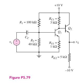
For each transistor in the circuit in Figure P5.79, \(\beta=120\) and the B-E turnon voltage is \(0.7 \mathrm{~V}\). Determine the quiescent base, collector, and emitter currents in \(Q_{1}\) and \(Q_{2}\). Also determine \(V_{C E Q 1}\) and \(V_{C E Q 2}\). +10 V R = 100 ks RC = 3 Q2 HH Figure
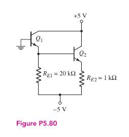
The parameters for each transistor in the circuit in Figure P5.80 are \(\beta=80\) and \(V_{B E}(\mathrm{on})=0.7 \mathrm{~V}\). Determine the quiescent values of base, collector, and emitter currents in \(Q_{1}\) and \(Q_{2}\). +5 V REI = 20 k2 RE2=1 k -5 V Figure P5.80
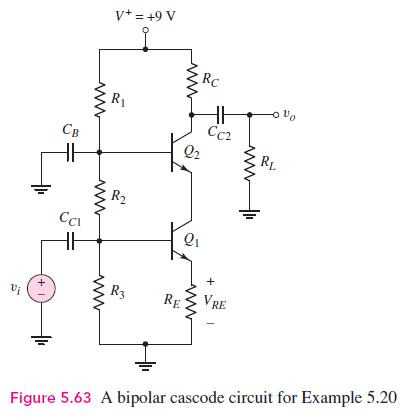
The bias voltage in the circuit shown in Figure 5.63 is changed to \(V^{+}=5 \mathrm{~V}\). Design the circuit to meet the following specifications: \(V_{C E 1}=V_{C E 2}=1.2 \mathrm{~V}, \quad V_{R E}=0.5 \mathrm{~V}, \quad I_{C 1} \cong I_{C 2} \cong 0.2\mathrm{~mA}, \quad\) and \(I_{R 1} \cong
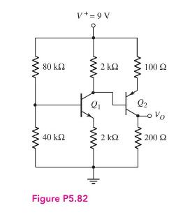
Consider the circuit shown in Figure P5.82. The current gain for the npn transistor is \(\beta_{n}=120\) and for the pnp transistor is \(\beta_{p}=80\). Determine \(I_{B 1}\), \(I_{C 1}, I_{B 2}, I_{C 2}, V_{C E 1}\), and \(V_{E C 2}\). V+=9V 80 2 100 22 - Vo 40 2 200 2 Figure P5.82
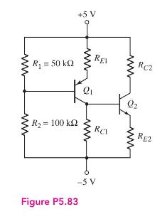
(a) For the transistors in the circuit shown in Figure P5.83, the parameters are: \(\beta=100\) and \(V_{B E}\) (on) \(=V_{E B}(\mathrm{on})=0.7 \mathrm{~V}\). Determine \(R_{C 1}, R_{E 1}, R_{C 2}\), and \(R_{E 2}\) such that \(I_{C 1}=I_{C 2}=0.8 \mathrm{~mA}, V_{E C Q 1}=3.5 \mathrm{~V}\), and
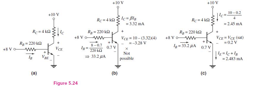
Using a computer simulation, plot \(V_{C E}\) versus \(V_{1}\) over the range \(0 \leq V_{I} \leq 8 \mathrm{~V}\) for the circuit in Figure 5.24(a). At what voltage does the transistor turn on and at what voltage does the transistor go into saturation? +8 V o +10 V +10 V Rc=4kQ 10-0.2 = 4 = 2.45 mA
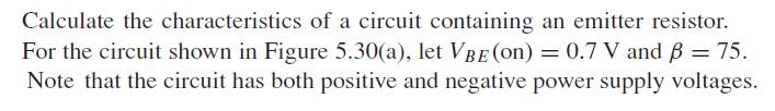
Using a computer simulation, verify the results of Example 5.7.Data From Example 5.7:-Figure 5.30(a):- Calculate the characteristics of a circuit containing an emitter resistor. For the circuit shown in Figure 5.30(a), let VBE (on) = 0.7 V and B = 75. Note that the circuit has both positive and
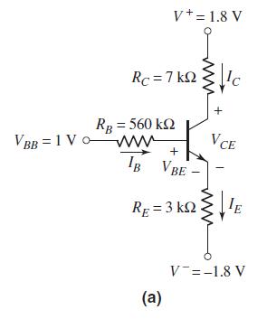
Consider the circuit and parameters in Example 5.15. Using a computer simulation, determine the change in \(Q\)-point values if all resistors vary by \(\pm 5\) percent.Data From Example 5.15:-Figure 5.54(a):- Analyze a circuit using a voltage divider bias circuit, and determine the change in the
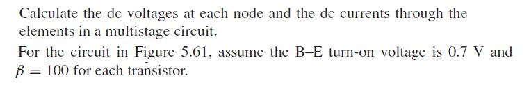
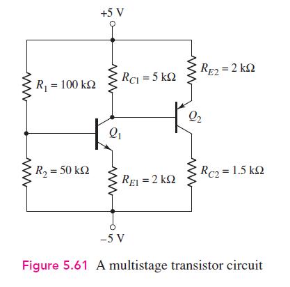
Using a computer simulation, verify the results of Example 5.19.Data From Example 5.19:-Figure 5.61:- Calculate the dc voltages at each node and the dc currents through the elements in a multistage circuit. For the circuit in Figure 5.61, assume the B-E turn-on voltage is 0.7 V and B = 100 for each
Consider a common-emitter circuit with the configuration shown in Figure 5.54(a). Assume a bias voltage of \(V_{C C}=3.3 \mathrm{~V}\) and assume the transistor current gain is in the range \(100 \leq \beta \leq 160\). Design the circuit such that the nominal \(Q\)-point is in the center of the
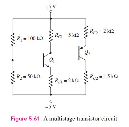
The emitter-follower circuit shown in Figure P5.89 is biased at \(V^{+}=2.5 \mathrm{~V}\) and \(V^{-}=-2.5 \mathrm{~V}\). Design a bias-stable circuit such that the nominal \(Q\)-point values are \(I_{C Q} \cong 5 \mathrm{~mA}\) and \(V_{C E Q} \cong 2.5\mathrm{~V}\). The transistor current gain
The bias voltages for the circuit in Figure 5.57 (a) are \(V^{+}=3.3 \mathrm{~V}\) and \(V^{-}=-3.3 \mathrm{~V}\). The transistor current gain is \(\beta=100\). Design a bias-stable circuit such that \(I_{C Q} \cong 120 \mu \mathrm{A}, V_{R E} \cong 0.7\mathrm{~V}\), and \(V_{E C Q} \cong 3
The multitransistor circuit in Figure 5.61 is to be redesigned. The bias voltages are to be \(\pm 3.3\mathrm{~V}\) and the nominal transistor current gains are \(\beta=120\). Design a bias-stable circuit such that \(I_{C Q 1}=100 \mu \mathrm{A}, I_{C Q 2}=200 \mu \mathrm{A}\), and \(V_{C E Q 1}
Discuss, using the concept of a load line, how a simple common-emitter circuit can amplify a time-varying signal.
Why can the analysis of a transistor circuit be split into a dc analysis, with all ac sources set equal to zero, and an ac analysis, with all dc sources set equal to zero?
What does the term small-signal imply?
Sketch the hybrid- \(\pi\) equivalent circuit of an npn and a pnp bipolar transistor.
State the relationships of the small-signal hybrid- \(\pi\) parameters \(g_{m}, r_{\pi}\), and \(r_{o}\) to the transistor dc quiescent values.
What are the physical meanings of the hybrid \(-\pi\) parameters \(r_{\pi}\) and \(r_{o}\) ?
Sketch a simple common-emitter amplifier circuit and discuss the general ac circuit characteristics (voltage gain, current gain, input and output resistances).
What are the changes in the dc and ac characteristics of a common-emitter amplifier when an emitter resistor and an emitter bypass capacitor are incorporated in the design?
Discuss the concepts of a dc load line and an ac load line.
Sketch a simple emitter-follower amplifier circuit and discuss the general ac circuit characteristics (voltage gain, current gain, input and output resistances).
Sketch a simple common-base amplifier circuit and discuss the general ac circuit characteristics (voltage gain, current gain, input and output resistances).
Compare the ac circuit characteristics of the common-emitter, emitter-follower, and common-base circuits.
Discuss the general conditions under which a common-emitter amplifier, an emitter-follower amplifier, and a common-base amplifier would be used in an electronic circuit design.
State at least two reasons why a multistage amplifier circuit would be required in a design rather than a single-stage circuit.
The parameters of the transistors in the circuit in Figure P4.56 are \(V_{T N D}=\) \(-1 \mathrm{~V}, K_{n D}=0.5 \mathrm{~mA} / \mathrm{V}^{2}\) for transistor \(M_{D}\), and \(V_{T N L}=+1 \mathrm{~V}, K_{n L}=\) \(30 \mu \mathrm{A} / \mathrm{V}^{2}\) for transistor \(M_{L}\). Assume
(a) Determine the built-in potential barrier \(V_{b i}\) in a silicon pn junction for (i) \(N_{d}=N_{a}=5 \times 10^{15} \mathrm{~cm}^{-3}\); (ii) \(N_{d}=5 \times 10^{17} \mathrm{~cm}^{-3}\) and \(N_{a}=10^{15} \mathrm{~cm}^{-3}\); (iii) \(N_{a}=N_{d}=10^{18} \mathrm{~cm}^{-3}\).(b) Repeat part
(a) The reverse-saturation current of a pn junction diode is \(I_{S}=10^{-11} \mathrm{~A}\). Determine the diode current for diode voltages of \(0.3,0.5,0.7,-0.02,-0.2\), and \(-2 \mathrm{~V}\).(b) Repeat part (a) for \(I_{S}=10^{-13} \mathrm{~A}\).
A silicon pn junction diode has an emission coefficient of \(n=1\). The diode current is \(I_{D}=1 \mathrm{~mA}\) when \(V_{D}=0.7 \mathrm{~V}\). (a) What is the reverse-bias saturation current? (b) Plot, on the same graph, \(\log _{10} I_{D}\) versus \(V_{D}\) over the range \(0.1 \leq V_{D} \leq
(a) Consider a silicon pn junction diode operating in the forward-bias region. Determine the increase in forward-bias voltage that will cause a factor of 10 increase in current.(b) Repeat part (a) for a factor of 100 increase in current.
The reverse-bias saturation current for a set of diodes varies between \(5 \times 10^{-14} \leq I_{S} \leq 5 \times 10^{-12} \mathrm{~A}\). The diodes are all to be biased at \(I_{D}=2 \mathrm{~mA}\). What is the range of forward-bias voltages that must be applied?
(a) The reverse-saturation current of a gallium arsenide pn junction diode is \(I_{S}=10^{-22} \mathrm{~A}\). Determine the diode current for diode voltages of \(0.8,1.0\), \(1.2,-0.02,-0.2\), and \(-2 \mathrm{~V}\).(b) Repeat part (a) for \(I_{S}=5 \times 10^{-24} \mathrm{~A}\).
A silicon pn junction diode has an applied forward-bias voltage of \(0.6 \mathrm{~V}\). Determine the ratio of current at \(100{ }^{\circ} \mathrm{C}\) to that at \(-55^{\circ} \mathrm{C}\).
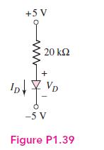
Consider the diode circuit shown in Figure P1.39. The diode reversesaturation current is \(I_{S}=10^{-12} \mathrm{~A}\). Determine the diode current \(I_{D}\) and diode voltage \(V_{D}\).Figure P1.39:- +5V 20 + ID VD -5 V Figure P1.39
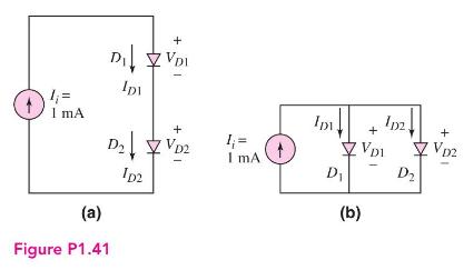
(a) For the circuit shown in Figure P1.41(a), determine \(I_{D 1}, I_{D 2}, V_{D 1}\), and \(V_{D 2}\) for (i) \(I_{S 1}=I_{S 2}=10^{-13} \mathrm{~A}\) and (ii) \(I_{S 1}=5 \times 10^{-14} \mathrm{~A}, I_{S 2}=5 \times 10^{-13} \mathrm{~A}\).(b) Repeat part (a) for the circuit shown in Figure
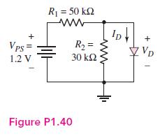
(a) Consider the circuit shown in Figure P1.40. The value of \(R_{1}\) is reduced to \(R_{1}=10 \mathrm{k} \Omega\) and the cut-in voltage of the diode is \(V_{\gamma}=0.7 \mathrm{~V}\). Determine \(I_{D}\) and \(V_{D}\).(b) Repeat part (a) if \(R_{1}=50 \mathrm{k} \Omega\).Figure P1.40:- + VPS=
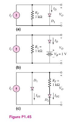
The diode cut-in voltage is \(V_{\gamma}=0.7 \mathrm{~V}\) for the circuits shown in Figure P1.45. Plot \(V_{O}\) and \(I_{D}\) versus \(I_{I}\) over the range \(0 \leq I_{I} \leq 2 \mathrm{~mA}\) for the circuit shown in (a) Figure P1.45(a), (b) Figure P1.45(b), and (c) Figure P1.45(c). (a) (b)
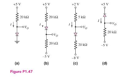
Find \(I\) and \(V_{O}\) in each circuit shown in Figure P1.47 if (i) \(V_{\gamma}=0.7 \mathrm{~V}\) and (ii) \(V_{\gamma}=0.6 \mathrm{~V}\). +5 V +5 V +2 V +5 V 5 20 20 Vo (a) Figure P1.47 -5 V (b) 20 k2 20 -5V -8 V (c) (d) ovo 20
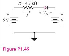
(a) In the circuit shown in Figure P1.49, find the diode voltage \(V_{D}\) and the supply voltage \(V\) such that the current is \(I_{D}=0.4 \mathrm{~mA}\). Assume the diode cut-in voltage is \(V_{\gamma}=0.7 \mathrm{~V}\). (b) Using the results of part (a), determine the power dissipated in the
(a) Consider a pn junction diode biased at \(I_{D Q}=1 \mathrm{~mA}\). A sinusoidal voltage is superimposed on \(V_{D Q}\) such that the peak-to-peak sinusoidal current is \(0.05 I_{D Q}\). Find the value of the applied peak-to-peak sinusoidal voltage.(b) Repeat part (a) if \(I_{D Q}=0.1
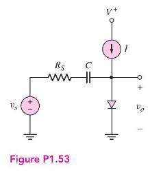
The diode in the circuit shown in Figure P1.53 is biased with a constant current source \(I\). A sinusoidal signal \(v_{s}\) is coupled through \(R_{S}\) and \(C\). Assume that \(C\) is large so that it acts as a short circuit to the signal. (a) Show that the sinusoidal component of the diode
A pn junction diode and a Schottky diode have equal cross-sectional areas and have forward-bias currents of \(0.5 \mathrm{~mA}\). The reverse-saturation current of the Schottky diode is \(I_{S}=5 \times 10^{-7} \mathrm{~A}\). The difference in forward-bias voltages between the two diodes is \(0.30
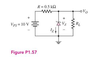
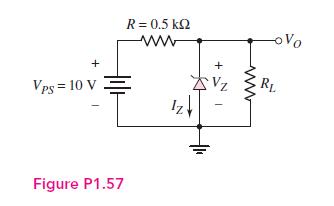
Consider the Zener diode circuit shown in Figure P1.57. The Zener breakdown voltage is \(V_{Z}=5.6 \mathrm{~V}\) at \(I_{Z}=0.1 \mathrm{~mA}\), and the incremental Zener resistance is \(r_{z}=10 \Omega\). (a) Determine \(V_{O}\) with no load \(\left(R_{L}=\infty\right)\). (b) Find the change in the
Consider the Zener diode circuit shown in Figure P1.57. The Zener diode voltage is \(V_{Z}=6.8 \mathrm{~V}\) at \(I_{Z}=0.1 \mathrm{~mA}\) and the incremental Zener resistance is \(r_{z}=20 \Omega\). (a) Calculate \(V_{O}\) with no load \(\left(R_{L}=\infty\right)\). (b) Find the change in the
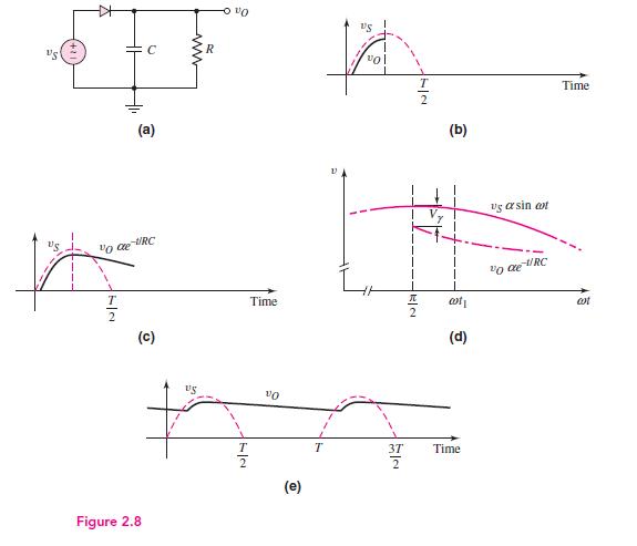
The parameters of the half-wave rectifier circuit in Figure 2.8 (a) in the text are \(R=1 \mathrm{k} \Omega, C=350 \mu \mathrm{F}\), and \(V_{\gamma}=0.7 \mathrm{~V}\). Assume \(v_{S}(t)=\) \(V_{S} \sin [2 \pi(60) t](\mathrm{V})\) where \(V_{S}\) is in the range of \(11 \leq V_{S} \leq 13
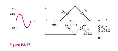
Sketch \(v_{o}\) versus time for the circuit in Figure P2.17 with the input shown. Assume \(V_{\gamma}=0\) Vi A +40 D R = 2.2 -40- Figure P2.17 www R = 2.2 ww R = 2.2
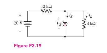
Consider the circuit shown in Figure P2.19. The Zener diode voltage is \(V_{Z}=3.9 \mathrm{~V}\) and the Zener diode incremental resistance is \(r_{z}=0\).(a) Determine \(I_{Z}, I_{L}\), and the power dissipated in the diode.(b) Repeat part (a) if the \(4 \mathrm{k} \Omega\) load resistor is
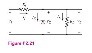
Consider the Zener diode circuit shown in Figure P2.21. Let \(V_{I}=60 \mathrm{~V}\), \(R_{i}=150 \Omega\), and \(V_{Z O}=15.4 \mathrm{~V}\). Assume \(r_{z}=0\). The power rating of the diode is \(4 \mathrm{~W}\) and the minimum diode current is to be \(15 \mathrm{~mA}\). (a) Determine the range of
A Zener diode is connected in a voltage regulator circuit as shown in Figure P2.21. The Zener voltage is \(V_{Z}=10 \mathrm{~V}\) and the Zener resistance is assumed to be \(r_{z}=0\). (a) Determine the value of \(R_{i}\) such that the Zener diode remains in breakdown if the load current varies
A voltage regulator is to have a nominal output voltage of \(10 \mathrm{~V}\). The specified Zener diode has a rating of \(1 \mathrm{~W}\), has a \(10 \mathrm{~V}\) drop at \(I_{Z}=25 \mathrm{~mA}\), and has a Zener resistance of \(r_{z}=5 \Omega\). The input power supply has a nominal value of
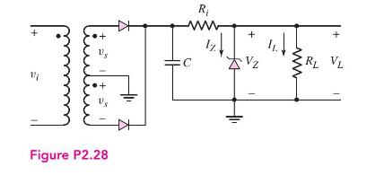
The secondary voltage in the circuit in Figure P2.28 is \(v_{s}=12 \sin \omega t \mathrm{~V}\). The Zener diode has parameters \(V_{Z}=8 \mathrm{~V}\) at \(I_{Z}=100 \mathrm{~mA}\) and \(r_{z}=0.5 \Omega\). Let \(V_{\gamma}=0\) and \(R_{i}=3 \Omega\). Determine the percent regulation for load
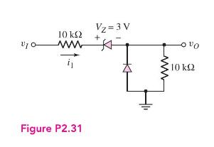
Consider the circuit in Figure P2.31. Let \(V_{\gamma}=0\). (a) Plot \(v_{O}\) versus \(v_{I}\) over the range \(-10 \leq v_{I} \leq+10 \mathrm{~V}\). (b) Plot \(i_{1}\) over the same input voltage range as part (a). 10 ww Figure P2.31 V2=3V 10
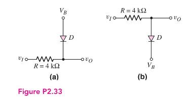
Each diode cut-in voltage is \(0.7 \mathrm{~V}\) for the circuits shown in Figure P2.33.(a) Plot \(v_{O}\) versus \(v_{I}\) over the range \(-5 \leq v_{I} \leq+5 \mathrm{~V}\) for the circuit in Figure P2.33 (a) for (i) \(V_{B}=1.8 \mathrm{~V}\) and (ii) \(V_{B}=-1.8 \mathrm{~V}\).(b) Repeat part
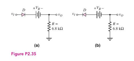
Consider the circuits shown in Figure P2.35. Each diode cut-in voltage is \(V_{\gamma}=0.7 \mathrm{~V}\).(a) Plot \(v_{O}\) versus \(v_{I}\) over the range \(-10 \leq v_{I} \leq+10 \mathrm{~V}\) for the circuit in Figure P2.35 (a) for (i) \(V_{B}=5 \mathrm{~V}\) and (ii) \(V_{B}=-5
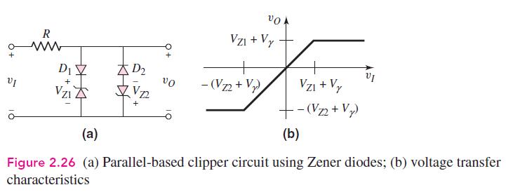
Consider the parallel clipper circuit in Figure 2.26 in the text. Assume \(V_{Z 1}=6 \mathrm{~V}, V_{Z 2}=4 \mathrm{~V}\), and \(V_{\gamma}=0.7 \mathrm{~V}\) for all diodes. For \(v_{I}=10 \sin \omega t\), sketch \(v_{O}\) versus time over two periods of the input signal. R www D VO VZ1 + Vy D2 VI
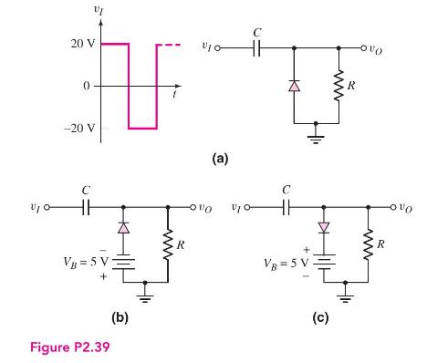
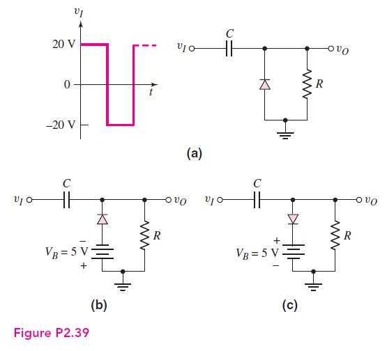
Sketch the steady-state output voltage \(v_{O}\) versus time for each circuit in Figure P2.39 with the input voltage given in Figure P2.39(a). Assume \(V_{\gamma}=0\) and assume the \(R C\) time constant is large. 20 V VI C HH 0 -20 V C HH (a) C VO ww R VB-5 V R VB-5 V R Figure P2.39 (b) (c) OVO
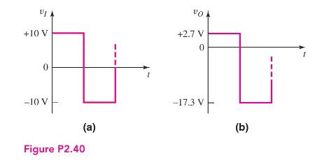
Design a diode clamper to generate a steady-state output voltage \(v_{0}\) from the input voltage \(v_{I}\) shown in Figure P2.40 if (a) \(V_{\gamma}=0\) and (b) \(V_{\gamma}=0.7 \mathrm{~V}\). VI +10 V vo +2.7 V 0 0 -10 V Figure P2.40 (a) -17.3 V (b)
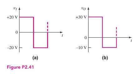
Design a diode clamper to generate a steady-state output voltage \(v_{O}\) from the input voltage \(v_{I}\) in Figure P2.41 if \(V_{\gamma}=0\). +20 V +30 V 0 -20 V Figure P2.41 (a) 0 -10 V (b)
Repeat Problem 2.42 for the circuit in Figure P2.39 (c) for (i) \(V_{B}=5 \mathrm{~V}\) and (ii) \(V_{B}=-5 \mathrm{~V}\).For the circuit in Figure P2.39(b), let \(V_{\gamma}=0\) and \(v_{I}=10 \sin \omega t(\mathrm{~V})\). Plot \(v_{O}\) versus time over three cycles of input voltage. Assume the
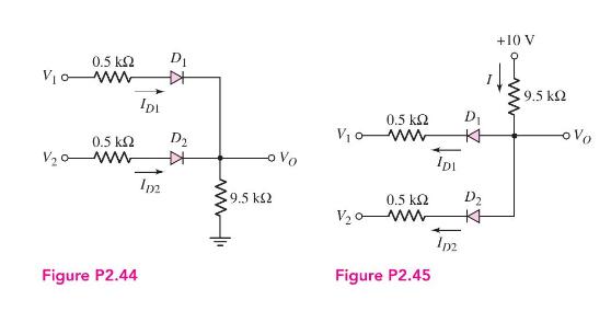
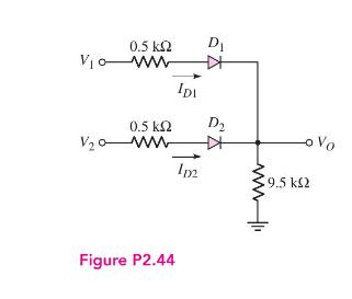
In the circuit in Figure P2.45 the diodes have the same piecewise linear parameters as described in Problem 2.44. Calculate the output voltage \(V_{O}\) and the currents \(I_{D 1}, I_{D 2}\), and \(I\) for the following input conditions:(a) \(V_{1}=\) \(V_{2}=10 \mathrm{~V}\);(b) \(V_{1}=10
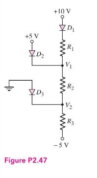
Consider the circuit shown in Figure P2.47. Assume each diode cut-in voltage is \(V_{\gamma}=0.6 \mathrm{~V}\).(a) Determine \(R_{1}, R_{2}\), and \(R_{3}\) such that \(I_{D 1}=0.2 \mathrm{~mA}\), \(I_{D 2}=0.3 \mathrm{~mA}\), and \(I_{D 3}=0.5 \mathrm{~mA}\).(b) Find \(V_{1}, V_{2}\), and each
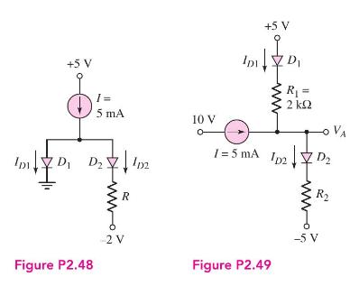
Consider the circuit in Figure P2.49. Each diode cut-in voltage is \(V_{\gamma}=0.7 \mathrm{~V}\).(a) For \(R_{2}=1.1 \mathrm{k} \Omega\), determine \(I_{D 1}, I_{D 2}\), and \(V_{A}\).(b) Repeat part (a) for \(R_{2}=2.5 \mathrm{k} \Omega\).(c) Find \(R_{2}\) such that \(V_{A}=0\). What are the
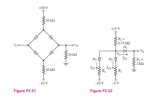
Assume \(V_{\gamma}=0.7 \mathrm{~V}\) for each diode in the circuit in Figure P2.51. Plot \(v_{O}\) versus \(v_{I}\) for \(-10 \leq v_{I} \leq+10 \mathrm{~V}\). +10 V 10 Figure P2.51 www 10 -10 V www 10 +15 V R = 6.15 D -o Vo VA D3 Dz Ip3 ID21 www- R = 2 RA R3 -10 V -5 V Figure P2.52
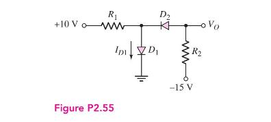
Assume each diode cut-in voltage is \(V_{\gamma}=0.7 \mathrm{~V}\) for the circuit in Figure P2.55. Determine \(I_{D 1}\) and \(V_{O}\) for (a) \(R_{1}=10 \mathrm{k} \Omega, R_{2}=5 \mathrm{k} \Omega\) and (b) \(R_{1}=5 \mathrm{k} \Omega, R_{2}=10 \mathrm{k} \Omega\). R D +10 Vo ww Vo IDI DI R -15
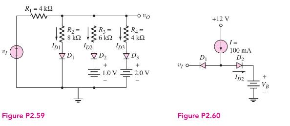
Each diode cut-in voltage in the circuit in Figure P2.59 is 0.7V. Determine \(I_{D 1}, I_{D 2}, I_{D 3}\), and \(v_{O}\) for (a) \(v_{I}=0.5 \mathrm{~V}\), (b) \(v_{I}=1.5 \mathrm{~V}\), (c) \(v_{I}=3.0 \mathrm{~V}\), and (d) \(v_{I}=5.0 \mathrm{~V}\). R = 4kQ ww Figure P2.59 R = 8 ID2 IDI D vo R
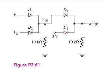
Consider the circuit in Figure P2.61. The output of a diode OR logic gate is connected to the input of a second diode OR logic gate. Assume \(V_{\gamma}=0.6 \mathrm{~V}\) for each diode. Determine the outputs \(V_{O 1}\) and \(V_{O 2}\) for: (a) \(V_{1}=V_{2}=0\); (b) \(V_{1}=5 \mathrm{~V},
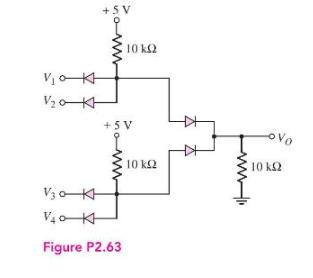
Determine the Boolean expression for \(V_{O}\) in terms of the four input voltages for the circuit in Figure P2.63. +5V Vo K V20KH 10 kQ +5V Vo K V40 KH Figure P2.63 10 kS2 www Vo 10 KS2
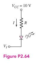
The light-emitting diode in the circuit shown in Figure P2.64 has parameters \(V_{\gamma}=1.7 \mathrm{~V}\) and \(r_{f}=0\). Light will first be detected when the current is \(I=8 \mathrm{~mA}\). If \(R=750 \Omega\), determine the value of \(V_{I}\) at which light will first be detected. Vcc = 10 V
(a) Calculate the drain current in an NMOS transistor with parameters \(V_{T N}=0.4 \mathrm{~V}, k_{n}^{\prime}=120 \mu \mathrm{A} / \mathrm{V}^{2}, W=10 \mu \mathrm{m}, L=0.8 \mu \mathrm{m}\), and with applied voltages of \(V_{D S}=0.1 \mathrm{~V}\) and (i) \(V_{G S}=0\), (ii) \(V_{G S}=1
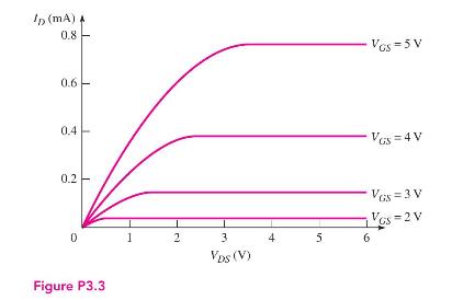
The transistor characteristics \(i_{D}\) versus \(v_{D S}\) for an NMOS device are shown in Figure P3.3. (a) Is this an enhancement-mode or depletion-mode device? (b) Determine the values for \(K_{n}\) and \(V_{T N}\). (c) Determine \(i_{D}\) (sat) for \(v_{G S}=3.5 \mathrm{~V}\) and \(v_{G S}=4.5
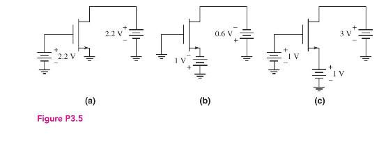
The threshold voltage of each transistor in Figure P3.5 is \(V_{T N}=0.4\) V. Determine the region of operation of the transistor in each circuit. 2.2 V 2.2 V Figure P3.5 (a) IV 0.6V 3V (b) (c)
Discuss, using the concept of a load line, how a simple common-source circuit can amplify a time-varying signal.
How does the transistor width-to-length ratio affect the small-signal voltage gain of a common-source amplifier?
Discuss the physical meaning of the small-signal circuit parameter \(r_{o}\).
How does the body effect change the small-signal equivalent circuit of the MOSFET?
Sketch a simple common-source amplifier circuit and discuss the general ac circuit characteristics (voltage gain and output resistance).
Discuss the general conditions under which a common-source amplifier would be used.
Why, in general, is the magnitude of the voltage gain of a common-source amplifier relatively small?
What are the changes in dc and ac characteristics of a common-source amplifier when a source resistor and a source bypass capacitor are incorporated in the design?
Showing 1300 - 1400
of 4723
First
7
8
9
10
11
12
13
14
15
16
17
18
19
20
21
Last
Step by Step Answers