New Semester
Started
Get
50% OFF
Study Help!
--h --m --s
Claim Now
Question Answers
Textbooks
Find textbooks, questions and answers
Oops, something went wrong!
Change your search query and then try again
S
Books
FREE
Study Help
Expert Questions
Accounting
General Management
Mathematics
Finance
Organizational Behaviour
Law
Physics
Operating System
Management Leadership
Sociology
Programming
Marketing
Database
Computer Network
Economics
Textbooks Solutions
Accounting
Managerial Accounting
Management Leadership
Cost Accounting
Statistics
Business Law
Corporate Finance
Finance
Economics
Auditing
Tutors
Online Tutors
Find a Tutor
Hire a Tutor
Become a Tutor
AI Tutor
AI Study Planner
NEW
Sell Books
Search
Search
Sign In
Register
study help
computer science
systems analysis and design 12th
Microelectronics Circuit Analysis And Design 4th Edition Donald A. Neamen - Solutions
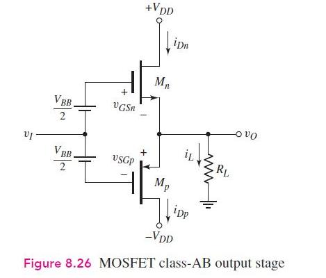
Consider the MOSFET class-AB output stage in Figure 8.26. The parameters are: \(V_{D D}=10 \mathrm{~V}\) and \(R_{L}=100 \Omega\). For transistors \(M_{n}\) and \(M_{p}, V_{T N}=\) \(-V_{T P}=1 \mathrm{~V}\). The peak amplitude of the output voltage is limited to \(5 \mathrm{~V}\). Design the
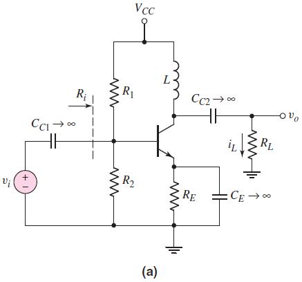
The parameters of the amplifier shown in Figure 8.28 (a) are \(V_{C C}=12 \mathrm{~V}\), \(R_{E}=20 \Omega, R_{1}=14 \mathrm{k} \Omega\), and \(R_{2}=10 \mathrm{k} \Omega\). The transistor parameters are \(\beta=90\) and \(V_{B E}\) (on) \(=0.7 \mathrm{~V}\).(a) Determine the quiescent value \(I_{C
For the inductively coupled amplifier in Figure 8.28(a), the parameters are: \(V_{C C}=15 \mathrm{~V}, R_{E}=0.1 \mathrm{k} \Omega\), and \(R_{L}=1 \mathrm{k} \Omega\). The transistor parameters are \(\beta=100\) and \(V_{B E}=0.7 \mathrm{~V}\). Design \(R_{1}\) and \(R_{2}\) to deliver the maximum
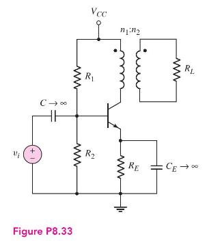
Consider the transformer-coupled common-emitter circuit shown in Figure P8.33 with parameters \(V_{C C}=12 \mathrm{~V}, R_{E}=20 \Omega, R_{L}=8 \Omega, R_{1}=\) \(2.3 \mathrm{k} \Omega\), and \(R_{2}=1.75 \mathrm{k} \Omega\). The transistor parameters are \(\beta=40\) and \(V_{B E}(\) on \()=0.7
The parameters for the transformer-coupled common-emitter circuit in Figure \(\mathrm{P} 8.33\) are \(V_{C C}=36 \mathrm{~V}\) and \(n_{1}: n_{2}=4: 1\). The signal power delivered to the load is \(2 \mathrm{~W}\). Determine: (a) the rms voltage across the load; (b) the rms voltage across the
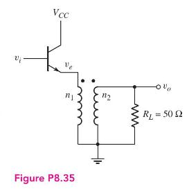
A BJT emitter follower is coupled to a load with an ideal transformer, as shown in Figure P8.35. The bias circuit is not shown. The transistor current gain is \(\beta=49\), and the transistor is biased such that \(I_{C Q}=100 \mathrm{~mA}\). (a) Derive the expressions for the voltage transfer
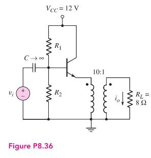
Consider the transformer-coupled emitter follower in Figure P8.36. Assume an ideal transformer. The transistor parameters are \(\beta=100\) and \(V_{B E}=\) \(0.7 \mathrm{~V}\). (a) Design the circuit to provide a current gain at \(A_{i}=i_{o} / i_{i}=80\). (b) If the magnitude of the signal
A class-A transformer-coupled emitter follower must deliver \(2 \mathrm{~W}\) to an \(8 \Omega\) speaker. Let \(V_{C C}=18 \mathrm{~V}, \beta=100\), and \(V_{B E}=0.7 \mathrm{~V}\). (a) Determine the required transformer ratio \(n_{1}: n_{2}\). (b) Determine the minimum transistor power rating.
Repeat Problem 8.36 if the primary side of the transformer has a resistance of \(100 \Omega\).Data From Problem 8.36:-Consider the transformer-coupled emitter follower in Figure P8.36. Assume an ideal transformer. The transistor parameters are \(\beta=100\) and \(V_{B E}=\) \(0.7 \mathrm{~V}\). (a)
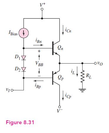
Consider the circuit in Figure 8.31. The circuit parameters are \(I_{\text {Bias }}=1 \mathrm{~mA}\), \(R_{L}=100 \Omega, V^{+}=10 \mathrm{~V}\), and \(V^{-}=-10 \mathrm{~V}\). The diode and transistor parameters are \(I_{S D}=5 \times 10^{-16} \mathrm{~A}\) and \(I_{S Q}=7 \times 10^{-15}
The circuit in Figure 8.31 is to be designed such that the quiescent collector currents are \(4 \mathrm{~mA}\left(v_{O}=0\right)\). Assume \(I_{S Q}=2 \times 10^{-15} \mathrm{~A}\) and \(I_{S D}=\) \(4 \times 10^{-16} \mathrm{~A}\). Neglecting base currents, (a) determine the required value of
The value of \(I_{\text {Bias }}\) in the circuit shown in Figure 8.31 is \(0.5 \mathrm{~mA}\). Assume diode and transistor parameters of \(I_{S D 1}=10^{-16} \mathrm{~A}, I_{S D 2}=4 \times 10^{-16} \mathrm{~A}\), \(I_{S Q_{n}}=8 \times 10^{-16} \mathrm{~A}\), and \(I_{S Q_{p}}=1.6 \times 10^{-15}
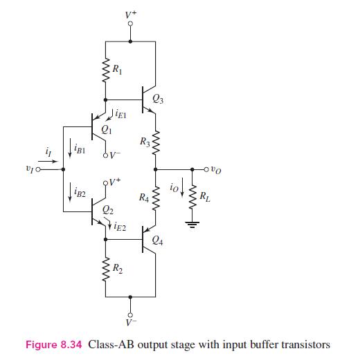
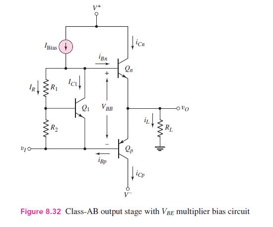
The transistors in the output stage in Figure 8.34 are all matched. Their parameters are \(\beta=60\) and \(I_{S}=5 \times 10^{-13} \mathrm{~A}\). Resistors \(R_{1}\) and \(R_{2}\) are replaced by \(3 \mathrm{~mA}\) ideal current sources, and \(R_{3}=R_{4}=0\). Let \(V^{+}=10 \mathrm{~V}\) and
Consider the circuit in Figure 8.34. The supply voltages are \(V^{+}=10 \mathrm{~V}\) and \(V^{-}=-10 \mathrm{~V}\), and the \(R_{3}\) and \(R_{4}\) resistor values are zero. The transistor parameters are: \(\beta_{1}=\beta_{2}=120, \beta_{3}=\beta_{4}=50, I_{S 1}=I_{S 2}=2 \times 10^{-13}
Using the parameters given in Example 8.11 for the circuit in Figure 8.34, calculate the input resistance when the quiescent output voltage is zero. iB1 www R JiEI 23 R3 iB2 R4 Q2 iE2 Q4 ww R 150 ww RL Figure 8.34 Class-AB output stage with input buffer transistors
(a) Redesign the class-AB output stage in Figure 8.34 using enhancementmode MOSFETs. Let \(R_{3}=R_{4}=0\). Sketch the circuit. (b) Assume bias voltages of \(V^{+}=10 \mathrm{~V}\) and \(V^{-}=-10 \mathrm{~V}\). Assume the threshold voltages of the \(\mathrm{n}\)-channel devices are \(V_{T N}=1
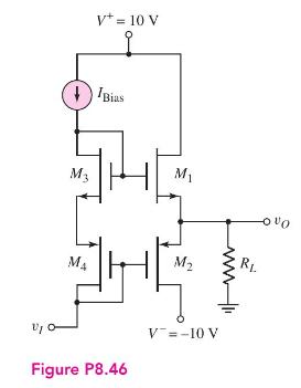
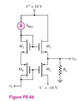
Consider the class-AB MOSFET output stage shown in Figure P8.46. The circuit parameters are \(I_{\text {Bias }}=0.2 \mathrm{~mA}\) and \(R_{L}=1 \mathrm{k} \Omega\). The transistor parameters are \(k_{n}^{\prime}=100 \mu \mathrm{A} / \mathrm{V}^{2}, k_{p}^{\prime}=40 \mu \mathrm{A} /
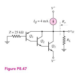
Figure P8.47 shows a composite pnp Darlington emitter follower that sinks current from a load. Parameter \(I_{Q}\) is the equivalent bias current and \(Z\) is the equivalent impedance in the base of \(Q_{1}\). Assume the transistor parameters are: \(\beta(\mathrm{pnp})=10, \beta(\mathrm{npn})=50,
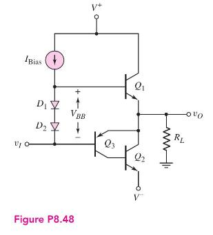
Consider the class-AB output stage in Figure P8.48. The parameters are: \(V^{+}=12 \mathrm{~V}, V^{-}=-12 \mathrm{~V}, R_{L}=100 \Omega\), and \(I_{\text {Bias }}=5 \mathrm{~mA}\). The transistor and diode parameters are \(I_{S}=10^{-13} \mathrm{~A}\). The transistor current gains are
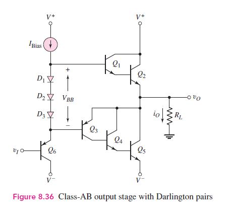
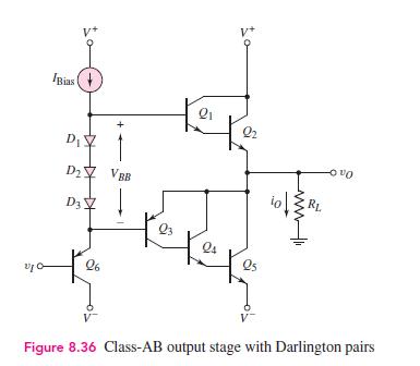
For the class-AB output stage in Figure 8.36, the parameters are: \(V^{+}=24 \mathrm{~V}, V^{-}=-24 \mathrm{~V}, R_{L}=20 \Omega\), and \(I_{\text {Bias }}=10 \mathrm{~mA}\). The diode and transistor parameters are \(I_{S}=2 \times 10^{-12} \mathrm{~A}\). The transistor current gains are
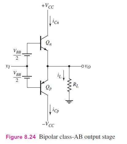
(a) Using a computer simulation, plot the voltage transfer characteristics of the complementary push-pull output stage shown in Figure 8.19 to demonstrate the crossover distortion.(b) Repeat part (a) for the class-AB output stage in Figure 8.24. Use several values of \(V_{B B}\). VI VBB 2 +VCC icn
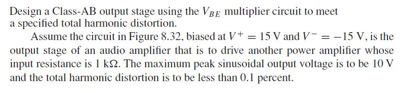
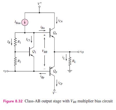
Using a computer simulation, plot the voltage transfer characteristics of the class-AB output stage with a \(V_{B E}\) multiplier bias circuit. Use the parameters described in Example 8.10.Data From Example 8.10:- Design a Class-AB output stage using the VBE multiplier circuit to meet a specified
Using a computer simulation, verify the results of Example 8.11.Data From Example 8.11:-Figure 8.34:- Determine the currents and the current gain for the output stage with input buffer transistors. = 100 For the circuit in Figure 8.34, the parameters are: R = R = 2 ks, RL 2, R3 = R4 = 0, and V+ =
Using a computer simulation, plot the voltage transfer characteristics of the class-AB output stage with Darlington pairs shown in Figure 8.36. Bias V+ V+ D D2 VBB D3 03 26 Q2 -00 RL Figure 8.36 Class-AB output stage with Darlington pairs
Design an audio amplifier to deliver an average of \(10 \mathrm{~W}\) to an \(8 \Omega\) speaker. The bandwidth is to cover the range from \(20 \mathrm{~Hz}\) to \(18 \mathrm{kHz}\). Specify minimum current gains, and current, voltage, and power ratings of all transistors.
Design a class-A transformer-coupled emitter-follower amplifier to deliver \(10 \mathrm{~W}\) to an \(8 \Omega\) speaker. The ambient temperature is \(25^{\circ} \mathrm{C}\) and the maximum junction temperature is \(T_{j, \max }=150^{\circ} \mathrm{C}\). Assume the thermal resistance values are:
Design the class-AB output stage with the \(V_{B E}\) multiplier in Figure 8.32 to deliver an average of \(1 \mathrm{~W}\) to an \(8 \Omega\) load. The peak output voltage must be no more than 80 percent of \(V^{+}\). Let \(V^{-}=-V^{+}\). Specify the circuit and transistor parameters. V+ Bias iBn
Design the circuit shown in Figure P8.46 to deliver \(2 \mathrm{~W}\) to a 20 ohm load. The maximum output voltage should be a symmetrical \(8 \mathrm{~V}\) sine wave. V+= 10 V +Bias M3 M -OVO M2 RL M4 Figure P8.46 V=-10 V
Describe the ideal op-amp model and describe the implications of this ideal model in terms of input currents and voltages.
Describe the op-amp model including the effect of a finite op-amp voltage gain.
Describe the operation and characteristics of the ideal inverting amplifier.
What is the concept of virtual ground?
What is the significance of a zero output resistance?
When a finite op-amp gain is taken into account, is the magnitude of the resulting amplifier voltage gain less than or greater than the ideal value?
Describe the operation and characteristics of the ideal summing amplifier.
Describe the operation and characteristics of the ideal noninverting amplifier.
Describe the voltage follower. What are the advantages of using this circuit.
What is the input resistance of an ideal current-to-voltage converter?
Describe the operation and characteristics of a difference amplifier.
Describe the operation and characteristics of an instrumentation amplifier.
Describe the operation and characteristics of an op-amp circuit using a capacitor as a feedback element.
Describe the operation and characteristics of an op-amp circuit using a diode as a feedback element.
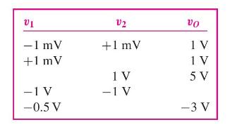
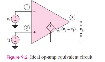
Assume an op-amp is ideal, except for having a finite open-loop differential gain. Measurements were made with the op-amp in the open-loop mode. Determine the open-loop gain and complete the following table, which shows the results of those measurements. Vi V2 vo -1 mV +1 mV 1 V +1 mV 1 V 1 V 5 V
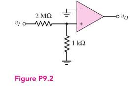
The op-amp in the circuit shown in Figure P9.2 is ideal except it has a finite open-loop gain. (a) If \(A_{o d}=10^{4}\) and \(v_{O}=-2 \mathrm{~V}\), determine \(v_{I}\). (b) If \(v_{I}=2 \mathrm{~V}\) and \(v_{O}=1 \mathrm{~V}\), determine \(A_{o d}\). UJ 2 www Figure P9.2 www 1
An op-amp is in an open-loop configuration as shown in Figure 9.2.(a) If \(v_{1}=2.0010 \mathrm{~V}, v_{2}=2.000 \mathrm{~V}\), and \(A_{o d}=5 \times 10^{3}\), determine \(v_{O}\).(b) If \(v_{2}=3.0025 \mathrm{~V}, v_{O}=-3.00 \mathrm{~V}\), and \(A_{o d}=2 \times 10^{4}\), what is \(v_{1}\) ?(c)
Consider the equivalent circuit of the op-amp shown in Figure 9.7(a). Assume terminal \(v_{1}\) is grounded and the input to terminal \(v_{2}\) is from a transducer that can be represented by a \(0.8 \mathrm{mV}\) voltage source in series with a \(25 \mathrm{k} \Omega\) resistance. What is the
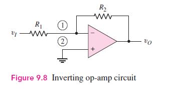
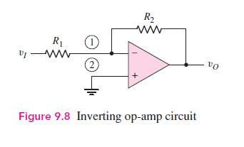
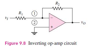
Consider the ideal inverting op-amp circuit shown in Figure 9.8. Determine the voltage gain \(A_{v}=v_{O} / v_{I}\) for(a) \(R_{2}=200 \mathrm{k} \Omega, R_{1}=20 \mathrm{k} \Omega\);(b) \(R_{2}=120 \mathrm{k} \Omega, R_{1}=40 \mathrm{k} \Omega\); and(c) \(R_{2}=40 \mathrm{k} \Omega, R_{1}=40
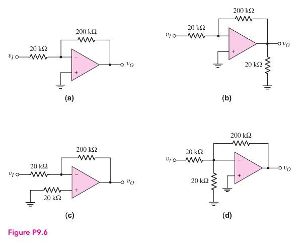
Assume the op-amps in Figure P9.6 are ideal. Find the voltage gain \(A_{v}=v_{O} / v_{I}\) and the input resistance \(R_{i}\) of each circuit. 20 www 200 www 20 k2 ww 200 ww 20 (a) www 20 Figure P9.6 (c) + (b) 20 200 www 20 200 www 20 (d) Vo
Consider an ideal inverting op-amp with \(R_{2}=100 \mathrm{k} \Omega\) and \(R_{1}=10 \mathrm{k} \Omega\).(a) Determine the ideal voltage gain and input resistance \(R_{i}\).(b) Repeat part (a) for a second \(100 \mathrm{k} \Omega\) resistor connected in parallel with \(R_{2}\).(c) Repeat part (a)
(a) Design an inverting op-amp circuit with a closed-loop voltage gain of \(A_{v}=v_{O} / v_{I}=-12\). The current in each resistor is to be no larger than \(20 \mu \mathrm{A}\) when the output voltage is \(-4.0 \mathrm{~V}\). (b) Using the results of part (a), determine \(v_{I}\) and the current
Consider an ideal op-amp used in an inverting configuration as shown in Figure 9.8. Determine the closed-loop voltage gain for the following resistor values.(a) \(R_{1}=20 \mathrm{k} \Omega, R_{2}=200 \mathrm{k} \Omega\)(b) \(R_{1}=20 \mathrm{k} \Omega, R_{2}=20 \mathrm{k} \Omega\)(c) \(R_{1}=20
Consider the inverting amplifier shown in Figure 9.8. Assume the op-amp is ideal. Determine the resistor values \(R_{1}\) and \(R_{2}\) to produce a closed-loop voltage gain of (a) -3.0 , (b) -8.0 , (c) -20 , and (d) -0.50 . In each case the largest resistor is to be limited to \(200 \mathrm{k}
(a) Design an inverting op-amp circuit with a closed-loop voltage gain of \(A_{v}=-6.5\). When in the input voltage is \(v_{I}=-0.25 \mathrm{~V}\), the magnitude of the currents is to be \(50 \mu \mathrm{A}\). Determine \(R_{1}\) and \(R_{2}\). (b) Using the results of part (a), find \(v_{I},
(a) Design an inverting op-amp circuit such that the closed-loop voltage gain is \(A_{v}=-20\) and the smallest resistor value is \(25 \mathrm{k} \Omega\).(b) Repeat part (a) for the case when the largest resistor value is \(1 \mathrm{M} \Omega\).(c) Determine \(i_{1}\) in both parts (a) and (b)
(a) In an inverting op-amp circuit, the nominal resistance values are \(R_{2}=300 \mathrm{k} \Omega\) and \(R_{1}=15 \mathrm{k} \Omega\). The tolerance of each resistor is \(\pm 5 \%\), which means that each resistance can deviate from its nominal value by \(\pm 5 \%\). What is the maximum
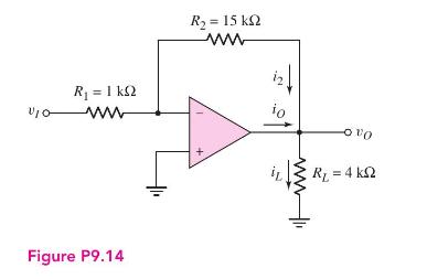
(a) The input to the circuit shown in Figure P9.14 is \(v_{I}=-0.20 \mathrm{~V}\). (i) What is \(v_{O}\) ? (ii) Determine \(i_{2}, i_{O}\), and \(i_{L}\).(b) Repeat part (a) for \(v_{I}=+0.05 \mathrm{~V}\).(c) Repeat part (a) for \(v_{I}=8 \sin \omega t \mathrm{mV}\). R = 1 k ww Figure P9.14 R = 15
Design an inverting amplifier to provide a nominal closed-loop voltage gain of \(A_{v}=-30\). The maximum input voltage signal is \(25 \mathrm{mV}\) with a source resistance in the range \(1 \mathrm{k} \Omega \leq R_{S} \leq 2 \mathrm{k} \Omega\). The variable source resistance should introduce no
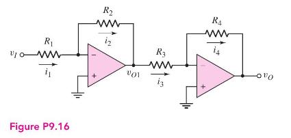
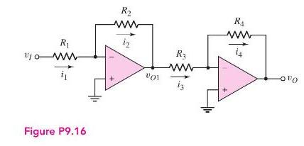
The parameters of the two inverting op-amp circuits connected in cascade in Figure P9.16 are \(R_{1}=10 \mathrm{k} \Omega, R_{2}=80 \mathrm{k} \Omega, R_{3}=20 \mathrm{k} \Omega\), and \(R_{4}=100 \mathrm{k} \Omega\). For \(v_{I}=-0.15 \mathrm{~V}\), determine \(v_{O 1}, v_{O}, i_{1}, i_{2},
Design the cascade inverting op-amp circuit in Figure P9.16 such that the overall closed-loop voltage gain is \(A_{v}=v_{O} / v_{I}=100\) and such that the maximum current in any resistor is limited to \(50 \mu \mathrm{A}\) when \(v_{I}=50 \mathrm{mV}\), but under the condition that the minimum
Design an amplifier system with three inverting op-amps circuits in cascade such that the overall closed-loop voltage gain is \(A_{v}=v_{O} / v_{I}=-300\). The maximum resistance is limited to \(200 \mathrm{k} \Omega\) and the minimum resistance is limited to \(20 \mathrm{k} \Omega\). In addition,
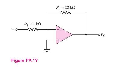
Consider the circuit shown in Figure P9.19. (a) Determine the ideal output voltage \(v_{O}\) if \(v_{I}=-0.40 \mathrm{~V}\). (b) Determine the actual output voltage if the open-loop gain of the op-amp is \(A_{o d}=5 \times 10^{3}\). (c) Determine the required value of \(A_{o d}\) in order that the
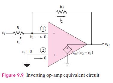
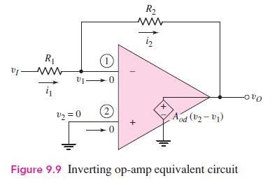
The inverting op-amp shown in Figure 9.9 has parameters \(R_{1}=25 \mathrm{k} \Omega\), \(R_{2}=100 \mathrm{k} \Omega\), and \(A_{o d}=5 \times 10^{3}\). The input voltage is from an ideal voltage source whose value is \(v_{I}=1.0000 \mathrm{~V}\). (a) Calculate the closed-loop voltage gain. (b)
(a) An op-amp with an open-loop gain of \(A_{o d}=7 \times 10^{3}\) is to be used in an inverting op-amp circuit. Let \(R_{2}=100 \mathrm{k} \Omega\) and \(R_{1}=10 \mathrm{k} \Omega\). If the output voltage is \(v_{O}=7 \mathrm{~V}\), determine the input voltage and the voltage at the inverting
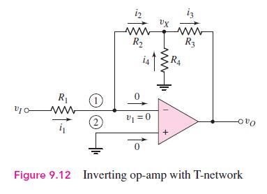
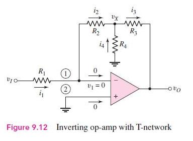
(a) For the ideal inverting op-amp circuit with T-network, shown in Figure 9.12, the circuit parameters are \(R_{1}=10 \mathrm{k} \Omega, R_{2}=R_{3}=50 \mathrm{k} \Omega\), and \(R_{4}=5 \mathrm{k} \Omega\). Determine the closed-loop voltage gain. (b) Determine a new value of \(R_{4}\) to produce
Consider the ideal inverting op-amp circuit with T-network in Figure 9.12. (a) Design the circuit such that the input resistance is \(500 \mathrm{k} \Omega\) and the gain is \(A_{v}=-80\). Do not use resistor values greater than \(500 \mathrm{k} \Omega\). (b) For the design in part (a), determine
An ideal inverting op-amp circuit is to be designed with a closed-loop voltage gain of \(A_{v}=-1000\). The largest resistor value to be used is \(500 \mathrm{k} \Omega\). (a) If the simple two-resistor design shown in Figure 9.8 is used, what is the input resistance? (b) If the T-network design
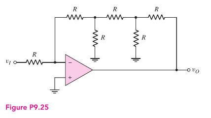
For the op-amp circuit shown in Figure P9.25, determine the gain \(A_{v}=v_{O} / v_{I}\). Compare this result to the gain of the circuit shown in Figure 9.12, assuming all resistor values are equal.Figure 9.12:- R www R R R ww ww ww Figure P9.25 www R
The inverting op-amp circuit in Figure 9.9 has parameters \(R_{1}=20 \mathrm{k} \Omega\), \(R_{2}=200 \mathrm{k} \Omega\), and \(A_{o d}=5 \times 10^{4}\). The output voltage is \(v_{O}=-4.80 \mathrm{~V}\). (a) Determine the closed-loop voltage gain. (b) Find the input voltage. (c) Determine the
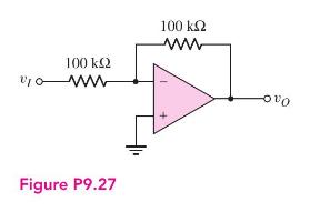
(a) Consider the op-amp circuit in Figure P9.27. The open-loop gain of the op-amp is \(A_{o d}=2.5 \times 10^{3}\). (i) Determine \(v_{O}\) when \(v_{I}=-0.80 \mathrm{~V}\). (ii) What is the percent error in output voltage compared to the ideal value?(b) Repeat part (a) for \(A_{o d}=200\). 100 ww
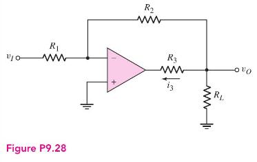
The circuit in Figure P9.28 is similar to the inverting amplifier except the resistor \(R_{3}\) has been added. (a) Derive the expression for \(v_{O}\) in terms of \(v_{I}\) and the resistors. (b) Derive the expression for \(i_{3}\) in terms of \(v_{I}\) and the resistors. Figure P9.28 R ww R www
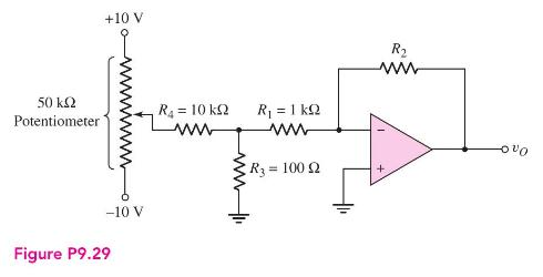
Design the amplifier in Figure P9.29 such that the output voltage varies between \(\pm 10 \mathrm{~V}\) as the wiper arm of the potentiometer changes from \(-10 \mathrm{~V}\) to \(+10 \mathrm{~V}\). What is the purpose of including \(R_{3}\) and \(R_{4}\) instead of connecting \(R_{1}\) directly to
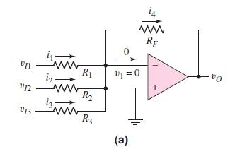
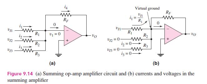
Consider the ideal inverting summing amplifier in Figure 9.14 (a) with parameters \(R_{1}=40 \mathrm{k} \Omega, R_{2}=20 \mathrm{k} \Omega, R_{3}=60 \mathrm{k} \Omega\), and \(R_{F}=120 \mathrm{k} \Omega\).(a) Determine \(v_{O}\) for \(v_{I 1}=-0.25 \mathrm{~V}, v_{I 2}=+0.10 \mathrm{~V}\), and
(a) Design an ideal inverting summing amplifier to produce an output voltage of \(v_{O}=-2.5\left(1.2 v_{I 1}+2.5 v_{I 2}+0.25 v_{I 3}\right)\). Design the circuit to produce the largest possible input resistance, assuming the largest resistance in the circuit is limited to \(400 \mathrm{k}
Design an ideal inverting summing amplifier to produce an output voltage of \(v_{O}=-2\left(v_{I 1}+3 v_{I 2}\right)\). The input voltages are limited to the ranges of \(-1 \leq v_{I 1} \leq+1 \mathrm{~V}\) and \(-0.5 \leq v_{I 2} \leq+0.2 \mathrm{~V}\). The current in any resistor is to be limited
Consider the summing amplifier in Figure 9.14 with \(R_{F}=10 \mathrm{k} \Omega\), \(R_{1}=1 \mathrm{k} \Omega, R_{2}=5 \mathrm{k} \Omega\), and \(R_{3}=10 \mathrm{k} \Omega\). If \(v_{I 1}\) is a \(1 \mathrm{kHz}\) sine wave with an rms value of \(50 \mathrm{mV}\), if \(v_{I 2}\) is a \(100
The parameters for the summing amplifier in Figure 9.14 are \(R_{F}=100 \mathrm{k} \Omega\) and \(R_{3}=\infty\). The two input voltages are \(v_{I 1}=4+125 \sin \omega t \mathrm{mV}\) and \(v_{I 2}=-6 \mathrm{mV}\). Determine \(R_{1}\) and \(R_{2}\) to produce an output voltage of \(v_{O}=-0.5
(a) Design an ideal summing op-amp circuit to provide an output voltage of \(v_{O}=-2\left[\left(v_{I 1} / 4\right)+2 v_{I 2}+v_{I 3}\right]\). The largest resistor value is to be \(250 \mathrm{k} \Omega\). (b) Using the results of part (a), determine the range in output voltage and the maximum
An ideal three-input inverting summing amplifier is to be designed. The input voltages are \(v_{I 1}=2+2 \sin \omega t \mathrm{~V}, v_{I 2}=0.5 \sin \omega t \mathrm{~V}\), and \(v_{I 3}=-4 \mathrm{~V}\). The desired output voltage is \(v_{O}=-6 \sin \omega t \mathrm{~V}\). The maximum current in
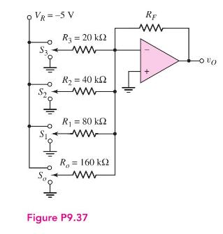
A summing amplifier can be used as a digital-to-analog converter (DAC). An example of a 4-bit DAC is shown in Figure P9.37. When switch \(S_{3}\) is connected to the \(-5 \mathrm{~V}\) supply, the most significant bit is \(a_{3}=1\); when \(S_{3}\) is connected to ground, the most significant bit
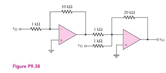
Consider the circuit in Figure P9.38. (a) Derive the expression for the output voltage \(v_{O}\) in terms of \(v_{I 1}\) and \(v_{I 2}\). (b) Determine \(v_{O}\) for \(v_{I 1}=+5 \mathrm{mV}\) and \(v_{I 2}=-25-50 \sin \omega t \mathrm{mV}\). (c) Determine the peak currents in the \(10 \mathrm{k}
Consider the summing amplifier in Figure 9.14 (a). Assume the op-amp has a finite open-loop differential gain \(A_{o d}\). Using the principle of superposition, show that the output voltage is given by\[v_{O}=\frac{-1}{1+\frac{\left(1+R_{F} / R_{P}\right)}{A_{o d}}}\left[\frac{R_{F}}{R_{1}} v_{I
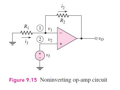
Consider the ideal noninverting op-amp circuit in Figure 9.15. Determine the closed-loop gain for the following circuit parameters: (a) \(R_{1}=15 \mathrm{k} \Omega\), \(R_{2}=150 \mathrm{k} \Omega\); (b) \(R_{1}=50 \mathrm{k} \Omega, R_{2}=150 \mathrm{k} \Omega\); (c) \(R_{1}=50 \mathrm{k} \Omega,
(a) Design an ideal noninverting op-amp circuit with the configuration shown in Figure 9.15 to have a closed-loop gain of \(A_{v}=15\). When \(v_{0}=-7.5 \mathrm{~V}\), the current in any resistor is to be limited to a maximum value of \(120 \mu \mathrm{A}\). (b) Using the results of part (a),
Consider the noninverting amplifier in Figure 9.15. Assume the op-amp is ideal. Determine the resistor values \(R_{1}\) and \(R_{2}\) to produce a closed-loop gain of (a) 3 , (b) 9 , (c) 30 and (d) 1.0. The maximum resistor value is to be limited to \(290 \mathrm{k} \Omega\). R 1 v1 ww (2) 12 iz ww
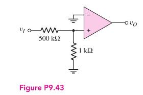
For the circuit in Figure P9.43, the input voltage is \(v_{I}=5 \mathrm{~V}\). (a) If \(v_{O}=2.5 \mathrm{~V}\), determine the finite open-loop differential gain of the op-amp. (b) If the open-loop differential gain of the op-amp is 5000 , determine \(v_{0}\). 500 Figure P9.43
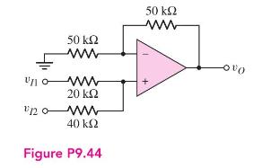
Determine \(v_{O}\) as a function of \(v_{I 1}\) and \(v_{I 2}\) for the ideal noninverting op-amp circuit in Figure P9.44. Un o 50 ww ww 20 2 ww 40 Figure P9.44 50 ww
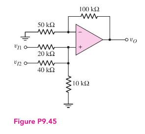
Consider the ideal noninverting op-amp circuit in Figure P9.45. (a) Derive the expression for \(v_{O}\) as a function of \(v_{I 1}\) and \(v_{I 2}\). (b) Find \(v_{O}\) for \(v_{I 1}=0.2 \mathrm{~V}\) and \(v_{I 2}=0.3 \mathrm{~V}\). (c) Find \(v_{0}\) for \(v_{I 1}=+0.25 \mathrm{~V}\) and \(v_{I
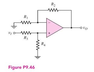
(a) Derive the expression for the closed-loop voltage gain \(A_{v}=v_{O} / v_{I}\) for the circuit shown in Figure P9.46. Assume an ideal op-amp. (b) Let \(R_{4}=50 \mathrm{k} \Omega\) and \(R_{3}=25 \mathrm{k} \Omega\). Determine \(R_{1}\) and \(R_{2}\) such that \(A_{v}=6\), assuming the maximum
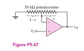
The circuit shown in Figure P9.47 can be used as a variable noninverting amplifier. The circuit uses a \(50 \mathrm{k} \Omega\) potentiometer in conjunction with an ideal op-amp. (a) Derive the expression for the closed-loop voltage gain \(v_{O} / v_{I}\) in terms of the potentiometer setting
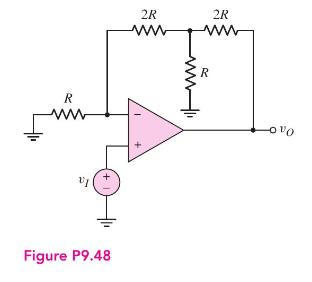
(a) Determine the closed-loop voltage gain \(A_{v}=v_{O} / v_{I}\) for the ideal opamp circuit in Figure P9.48. (b) Determine \(v_{O}\) for \(v_{I}=0.25 \mathrm{~V}\). (c) Let \(R=30 \mathrm{k} \Omega\). For \(v_{I}=-0.15 \mathrm{~V}\), determine the current in the resistor \(R\) in the T-network.
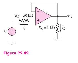
For the amplifier in Figure P9.49, determine (a) the ideal closed-loop voltage gain, (b) the actual closed-loop voltage gain if the open-loop gain is \(A_{o d}=150,000\), and (c) the open-loop gain such that the actual closed-loop gain is within 1 percent of the ideal. Ono + Rs = 50 k2 www R = 1 kQ
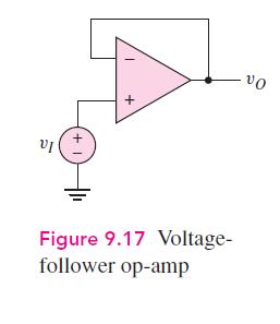
Consider the voltage-follower circuit in Figure 9.17. Determine the closed-loop voltage gain if the op-amp open-loop voltage gain \(A_{o d}\) is (a) 20, (b) 200 ,(c) \(2 \times 10^{3}\), and (d) \(2 \times 10^{4}\). VI 1+ + Figure 9.17 Voltage- follower op-amp -vo
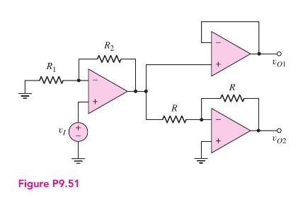
(a) Consider the ideal op-amp circuit shown in Figure P9.51. Determine the voltage gains \(A_{v 1}=v_{O 1} / v_{I}\) and \(A_{v 2}=v_{O 2} / v_{I}\). What is the relationship between \(v_{O 1}\) and \(v_{O 2}\) ? (b) For \(R_{2}=60 \mathrm{k} \Omega, R_{1}=20 \mathrm{k} \Omega\), and \(R=50
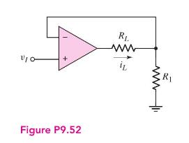
(a) Assume the op-amp in the circuit in Figure P9.52 is ideal. Determine \(i_{L}\) as a function of \(v_{I}\). (b) Let \(R_{1}=9 \mathrm{k} \Omega\) and \(R_{L}=1 \mathrm{k} \Omega\). If the op-amp saturates at \(\pm 10 \mathrm{~V}\), determine the maximum value of \(v_{I}\) and \(i_{L}\) before
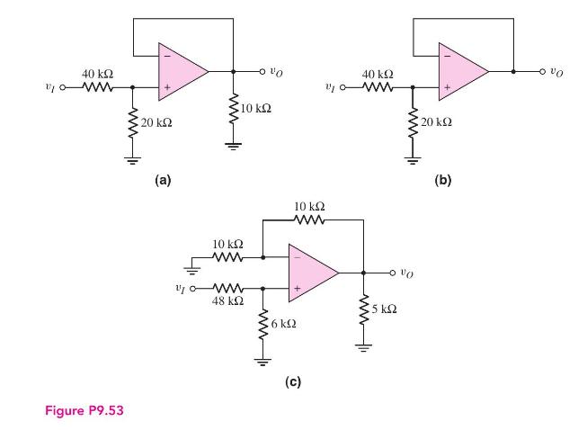
Consider the three circuits shown in Figure P9.53. Determine each output voltage for (i) \(v_{I}=3 \mathrm{~V}\) and (ii) \(v_{I}=-5 \mathrm{~V}\). 40 ww ww 20 10 (a) 40 ww www 20 10 10 www (b) ww ww 48 ww 6 k2 Figure P9.53 (c) www 5 - VO
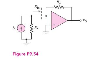
A current-to-voltage converter is shown in Figure P9.54. The current source has a finite output resistance \(R_{S}\), and the op-amp has a finite open-loop differential gain \(A_{o d}\). (a) Show that the input resistance is given by\[R_{\mathrm{in}}=\frac{R_{F}}{1+A_{o d}}\](b) If \(R_{F}=10
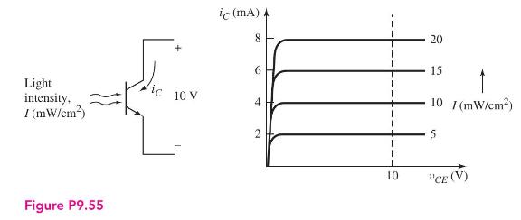
Figure P9.55 shows a phototransistor that converts light intensity into an output current. The transistor must be biased as shown. The transistor output versus input characteristics are shown. Design a current-to-voltage converter to produce an output voltage between 0 and \(8 \mathrm{~V}\) for an
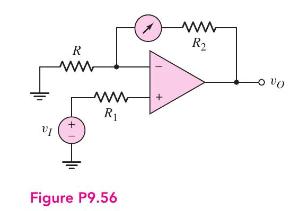
The circuit in Figure P9.56 is an analog voltmeter in which the meter reading is directly proportional to the input voltage \(v_{I}\). Design the circuit such that a \(1 \mathrm{~mA}\) full-scale reading corresponds to \(v_{I}=10 \mathrm{~V}\). Resistance \(R_{2}\) corresponds to the meter
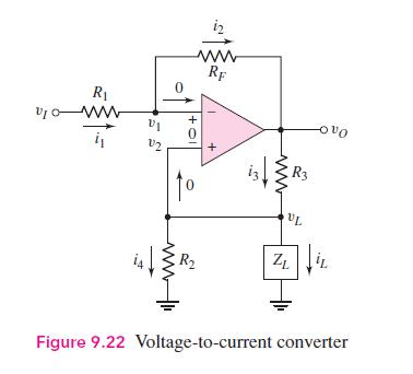
Consider the voltage-to-current converter in Figure 9.22 using an ideal opamp. (a) Design the circuit such that the current in a \(200 \Omega\) load can be varied between 0 and \(5 \mathrm{~mA}\) with an input voltage between 0 and \(-5 \mathrm{~V}\). Assume the op-amp is biased at \(\pm 15
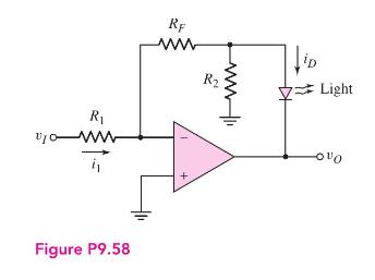
The circuit in Figure P9.58 is used to drive an LED with a voltage source. The circuit can also be thought of as a current amplifier in that, with the proper design, \(i_{D}>i_{1}\). (a) Derive the expression for \(i_{D}\) in terms of \(i_{1}\) and the resistors. (b) Design the circuit such that
Showing 900 - 1000
of 4723
First
3
4
5
6
7
8
9
10
11
12
13
14
15
16
17
Last
Step by Step Answers