New Semester
Started
Get
50% OFF
Study Help!
--h --m --s
Claim Now
Question Answers
Textbooks
Find textbooks, questions and answers
Oops, something went wrong!
Change your search query and then try again
S
Books
FREE
Study Help
Expert Questions
Accounting
General Management
Mathematics
Finance
Organizational Behaviour
Law
Physics
Operating System
Management Leadership
Sociology
Programming
Marketing
Database
Computer Network
Economics
Textbooks Solutions
Accounting
Managerial Accounting
Management Leadership
Cost Accounting
Statistics
Business Law
Corporate Finance
Finance
Economics
Auditing
Tutors
Online Tutors
Find a Tutor
Hire a Tutor
Become a Tutor
AI Tutor
AI Study Planner
NEW
Sell Books
Search
Search
Sign In
Register
study help
computer science
systems analysis and design 12th
Microelectronics Circuit Analysis And Design 4th Edition Donald A. Neamen - Solutions
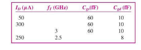
Fill in the missing parameter values in the following table for a MOSFET. Let \(K_{n}=1.5 \mathrm{~mA} / \mathrm{V}^{2}\). ID (A) fr (GHz) Cgs(fF) Cgd (FF) 50 60 10 300 60 10 3 60 10 250 2.5 8
(a) An n-channel MOSFET has an electron mobility of \(450 \mathrm{~cm}^{2} / \mathrm{V}-\mathrm{s}\) and a channel length of \(1.2 \mu \mathrm{m}\). Let \(V_{G S}-V_{T N}=0.5 \mathrm{~V}\). Determine the cutoff frequency \(f_{T}\).(b) Repeat part (a) if the channel length is reduced to \(0.18 \mu
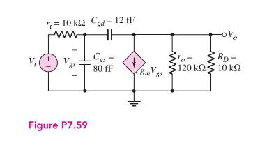
A common-source equivalent circuit is shown in Figure P7.59. The transistor transconductance is \(g_{m}=3 \mathrm{~mA} / \mathrm{V}\). (a) Calculate the equivalent Miller capacitance. (b) Determine the upper \(3 \mathrm{~dB}\) frequency for the small-signal voltage gain. = 10 k2 Cd 12 fF HH +1 " V.
Starting with the definition of unity-gain frequency, as given by Equation (7.97), neglect the overlap capacitance, assume \(C_{g d} \cong 0\) and \(C_{g s} \cong\) \(\left(\frac{2}{3}\right) W L C_{\text {ox }}\), and show that\(f_{T}=\frac{3}{2 \pi L} \cdot \sqrt{\frac{\mu_{n} I_{D}}{2
The parameters of an ideal n-channel MOSFET are \(W / L=8\), \(\mu_{n}=400 \mathrm{~cm}^{2} / \mathrm{V}-\mathrm{s}, C_{\mathrm{ox}}=6.9 \times 10^{-7} \mathrm{~F} / \mathrm{cm}^{2}\), and \(V_{T N}=0.4 \mathrm{~V}\). (a) Determine the maximum source resistance such that the transconductance
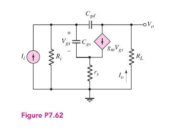
Figure P7.62 shows the high-frequency equivalent circuit of an FET, including a source resistance \(r_{s}\). (a) Derive an expression for the lowfrequency current gain \(A_{i}=I_{o} / I_{i}\). (b) Assuming \(R_{i}\) is very large, derive an expression for the current gain transfer function
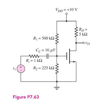
For the FET circuit in Figure P7.63, the transistor parameters are: \(K_{n}=\) \(1 \mathrm{~mA} / \mathrm{V}^{2}, V_{T N}=2 \mathrm{~V}, \lambda=0, C_{g s}=50 \mathrm{fF}\), and \(C_{g d}=8 \mathrm{fF}\). (a) Draw the simplified high-frequency equivalent circuit. (b) Calculate the equivalent Miller
The midband voltage gain of a common-source MOSFET amplifier is \(A_{v}=-15 \mathrm{~V} / \mathrm{V}\). The capacitances of the transistor are \(C_{g s}=0.2 \mathrm{pF}\) and \(C_{g d}=0.04 \mathrm{pF}\). (a) Determine the input Miller capacitance. (b) What equivalent input resistance (bias
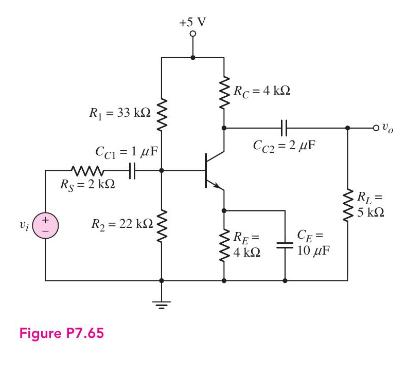
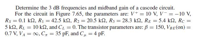
In the circuit in Figure P7.65, the transistor parameters are: \(\beta=120\), \(V_{B E}(\) on \()=0.7 \mathrm{~V}, V_{A}=100 \mathrm{~V}, C_{\mu}=1 \mathrm{pF}\), and \(f_{T}=600 \mathrm{MHz}\). (a) Determine \(C_{\pi}\) and the equivalent Miller capacitance \(C_{M}\). State any approximations or
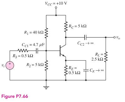
In the circuit in Figure P7.66, the transistor parameters are: \(\beta=120\), \(V_{B E}(\mathrm{on})=0.7 \mathrm{~V}, V_{A}=\infty, C_{\mu}=3 \mathrm{pF}\), and \(f_{T}=250 \mathrm{MHz}\). Assume the emitter bypass capacitor \(C_{E}\) and the coupling capacitor \(C_{C 2}\) are very large. (a)
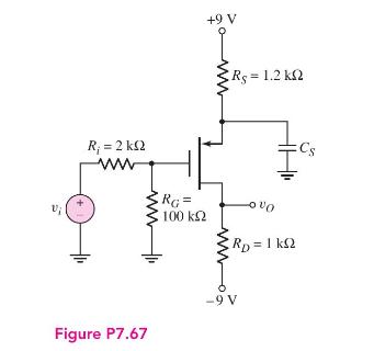
The parameters of the transistor in the common-source circuit in Figure P7.67 are: \(K_{p}=2 \mathrm{~mA} / \mathrm{V}^{2}, V_{T P}=-2 \mathrm{~V}, \lambda=0.01 \mathrm{~V}^{-1}, C_{g s}=10 \mathrm{pF}\), and \(C_{g d}=1 \mathrm{pF}\). (a) Determine the equivalent Miller capacitance \(C_{M}\). (b)
The bias voltages of the circuit shown in Figure P7.67 are changed to \(V^{+}=3 \mathrm{~V}\) and \(V^{-}=-3 \mathrm{~V}\). The input resistances are \(R_{i}=4 \mathrm{k} \Omega\) and \(R_{G}=200 \mathrm{k} \Omega\). The transistor parameters are \(K_{p}=0.5 \mathrm{~mA} / \mathrm{V}^{2}, V_{T
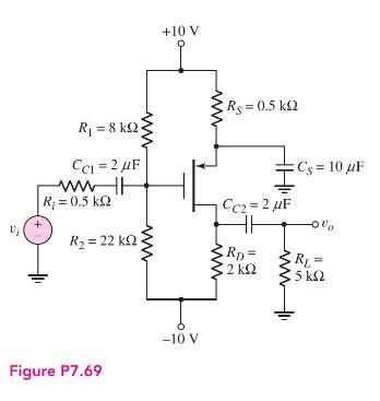
For the PMOS common-source circuit shown in Figure P7.69, the transistor parameters are: \(V_{T P}=-2 \mathrm{~V}, K_{p}=1 \mathrm{~mA} / \mathrm{V}^{2}, \lambda=0, C_{g s}=15 \mathrm{pF}\), and \(C_{g d}=3 \mathrm{pF}\). (a) Determine the upper \(3 \mathrm{~dB}\) frequency. (b) What is the
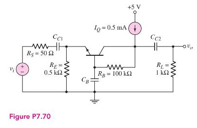
In the common-base circuit shown in Figure P7.70, the transistor parameters are: \(\beta=100, V_{B E}(\) on \()=0.7 \mathrm{~V}, V_{A}=\infty, C_{\pi}=10 \mathrm{pF}\), and \(C_{\mu}=1 \mathrm{pF}\). (a) Determine the upper \(3 \mathrm{~dB}\) frequencies corresponding to the input and output
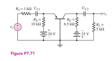
Repeat Problem 7.70 for the common-base circuit in Figure P7.71. Assume \(V_{E B}(\) on \()=0.7\) for the pnp transistor. The remaining transistor parameters are the same as given in Problem 7.70.Figure P7.71:-Data From Problem 7.70:-In the common-base circuit shown in Figure P7.70, the transistor
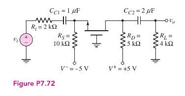
In the common-gate circuit in Figure P7.72, the transistor parameters are: \(V_{T N}=1 \mathrm{~V}, K_{n}=3 \mathrm{~mA} / \mathrm{V}^{2}, \lambda=0, C_{g s}=15 \mathrm{pF}\), and \(C_{g d}=4 \mathrm{pF}\). Determine the upper \(3 \mathrm{~dB}\) frequency and midband voltage gain. CC = 1 F ww R = 2
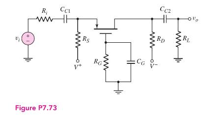
Consider the common-gate circuit in Figure P7.73 with parameters \(V^{+}=\) \(5 \mathrm{~V}, V^{-}=-5 \mathrm{~V}, R_{S}=4 \mathrm{k} \Omega, R_{D}=2 \mathrm{k} \Omega, R_{L}=4 \mathrm{k} \Omega, R_{G}=50 \mathrm{k} \Omega\), and \(R_{i}=0.5 \mathrm{k} \Omega\). The transistor parameters are:
For the cascode circuit in Figure 7.65 in the text, circuit parameters are the same as described in Example 7.15. The transistor parameters are: \(\beta_{o}=120, V_{A}=\infty, V_{B E}(\mathrm{on})=0.7 \mathrm{~V}, C_{\pi}=12 \mathrm{pF}\), and \(C_{\mu}=2 \mathrm{pF}\). (a) If \(C_{L}\) is an open
An emitter-follower amplifier is shown in Figure P7.75. Using a computer simulation, determine the upper \(3 \mathrm{~dB}\) frequency and the midband voltage gain for: (a) \(R_{L}=0.2 \mathrm{k} \Omega\), (b) \(R_{L}=2 \mathrm{k} \Omega\), and (c) \(R_{L}=20 \mathrm{k} \Omega\). Use a standard
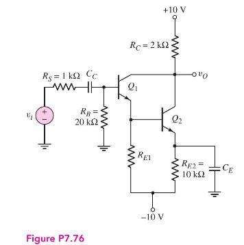
The transistor circuit in Figure P7.76 is a Darlington pair configuration. Using a computer simulation, determine the upper \(3 \mathrm{~dB}\) frequency and the midband voltage gain for (a) \(R_{E 1}=10 \mathrm{k} \Omega\), (b) \(R_{E 1}=40 \mathrm{k} \Omega\), and (c) \(R_{E 1}=\infty\). Use
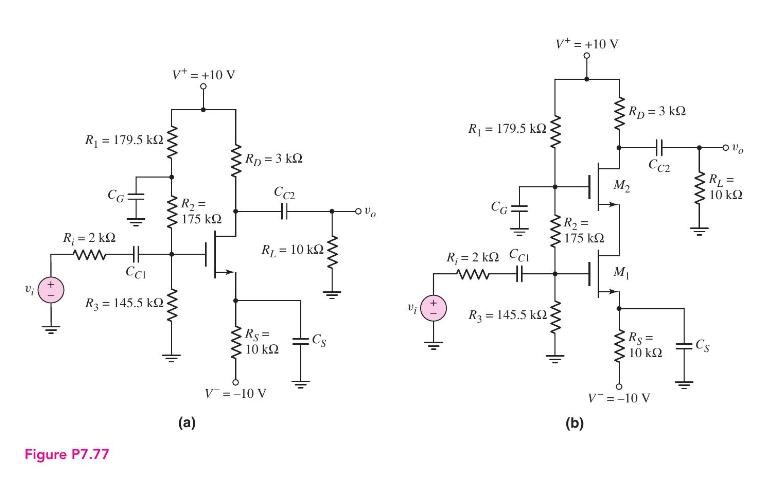
Consider the common-source amplifier in Figure P7.77 (a) and the cascode amplifier in Figure P7.77(b). Using standard transistors, determine the upper \(3 \mathrm{~dB}\) frequency and the midband voltage gain for each circuit using a computer simulation. Compare the \(3 \mathrm{~dB}\) frequencies
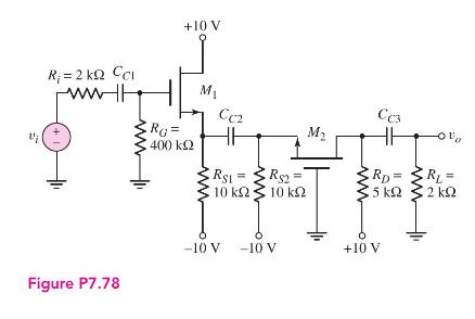
Consider identical transistors in the circuit in Figure P7.78. Assume the two coupling capacitors are both equal to \(C_{C}=4.7 \mu \mathrm{F}\). Using a computer simulation, determine the lower and upper \(3 \mathrm{~dB}\) frequencies as well as the midband gain. What value of load capacitance
(a) Design a common-emitter amplifier using a 2N2222A transistor biased at \(I_{C Q}=1 \mathrm{~mA}\) and \(V_{C E Q}=10 \mathrm{~V}\). The available power supplies are \(\pm 15 \mathrm{~V}\), the load resistance is \(R_{L}=20 \mathrm{k} \Omega\), the source resistance is \(R_{S}=0.5 \mathrm{k}
Design a bipolar amplifier with a midband gain of \(\left|A_{v}\right|=50\) and a lower \(3 \mathrm{~dB}\) frequency of \(10 \mathrm{~Hz}\). The available transistors are \(2 \mathrm{~N} 2222 \mathrm{~A}\), and the available power supplies are \(\pm 10 \mathrm{~V}\). All transistors in the circuit
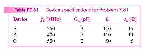
A common-emitter amplifier is designed to provide a particular midband gain and a particular bandwidth, using device A from Table P7.81. Assume \(I_{C Q}=1 \mathrm{~mA}\). Investigate the effect on midband gain and bandwidth if devices B and C are inserted into the circuit. Which device provides
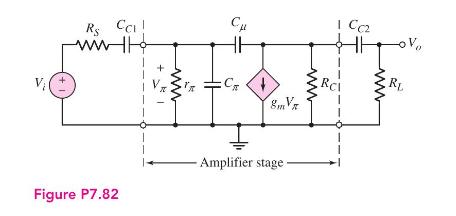
A simplified high-frequency equivalent circuit of a common-emitter amplifier is shown in Figure P7.82. The input signal is coupled into the amplifier through \(C_{C 1}\), the output signal is coupled to the load through \(C_{C 2}\), and the amplifier provides a midband gain of
Describe the basic structure and operation of npn and pnp bipolar transistors.
What are the bias voltages that need to be applied to an npn bipolar transistor such that the transistor is biased in the forward-active mode?
Define the conditions for cutoff, forward-active mode, and saturation mode for a pnp bipolar transistor.
Define common-base current gain and common-emitter current gain.
Discuss the difference between the ac and dc common-emitter current gains.
State the relationships between collector, emitter, and base currents in a bipolar transistor biased in the forward-active mode.
Define Early voltage and collector output resistance.
Describe a simple common-emitter circuit with an npn bipolar transistor and discuss the relation between collector-emitter voltage and input base current.
Describe the parameters that define a load line. Define \(Q\)-point.
What are the steps used to analyze the dc response of a bipolar transistor circuit?
Describe how an npn transistor can be used to switch an LED diode on and off.
Describe a bipolar transistor NOR logic circuit.
Describe how a transistor can be used to amplify a time-varying voltage.
Discuss the advantages of using resistor voltage divider biasing compared to a single base resistor.
What is the principal difference between biasing techniques used in discrete transistor circuits and integrated circuits?
(a) In a bipolar transistor biased in the forward-active region, the base current is \(i_{B}=2.8 \mu \mathrm{A}\) and the emitter current is \(i_{E}=325 \mu \mathrm{A}\). Determine \(\beta\), \(\alpha\), and \(i_{C}\).(b) Repeat part (a) if \(i_{B}=20 \mu \mathrm{A}\) and \(i_{E}=1.80
(a) A bipolar transistor is biased in the forward-active mode. The collector current is \(i_{C}=726 \mu \mathrm{A}\) and the emitter current is \(i_{E}=732 \mu \mathrm{A}\). Determine \(\beta, \alpha\), and \(i_{B}\).(b) Repeat part (a) if \(i_{C}=2.902 \mathrm{~mA}\) and \(i_{E}=2.961
(a) The range of \(\beta\) for a particular type of transistor is \(110 \leq \beta \leq 180\). Determine the corresponding range of \(\alpha\). (b) If the base current is \(50 \mu \mathrm{A}\), determine the range of collector current.
(a) A bipolar transistor is biased in the forward-active mode. The measured parameters are \(i_{E}=1.25 \mathrm{~mA}\) and \(\beta=150\). Determine \(i_{B}, i_{C}\), and \(\alpha\).(b) Repeat part (a) for \(i_{E}=4.52 \mathrm{~mA}\) and \(\beta=80\).
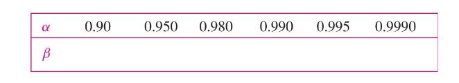
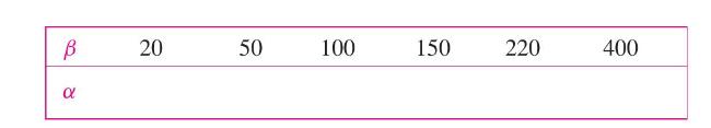
(a) For the following values of common-base current gain \(\alpha\), determine the corresponding common-emitter current gain \(\beta\) :(b) For the following values of common-emitter current gain \(\beta\), determine the corresponding common-base current gain \(\alpha\) : 0.90 0.950 0.980 0.990
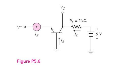
An npn transistor with \(\beta=80\) is connected in a common-base configuration as shown in Figure P5.6.(a) The emitter is driven by a constant-current source with \(I_{E}=1.2 \mathrm{~mA}\). Determine \(I_{B}, I_{C}, \alpha\), and \(V_{C}\).(b) Repeat part (a) for \(I_{E}=0.80 \mathrm{~mA}\).(c)
The emitter current in the circuit in Figure P5.6 is \(I_{E}=0.80 \mathrm{~mA}\). The transistor parameters are \(\alpha=0.9910\) and \(I_{E O}=5 \times 10^{-14} \mathrm{~A}\). Determine \(I_{B}\), \(I_{C}, V_{B E}\), and \(V_{C}\). Vc RC=2 k ww + 5 V Ic IE Figure P5.6
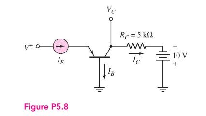
A pnp transistor with \(\beta=60\) is connected in a common-base configuration as shown in Figure P5.8.(a) The emitter is driven by a constant-current source with \(I_{E}=0.75 \mathrm{~mA}\). Determine \(I_{B}, I_{C}, \alpha\), and \(V_{C}\).(b) Repeat part (a) if \(I_{E}=1.5 \mathrm{~mA}\).(c) Is
(a) The pnp transistor shown in Figure P5.8 has a common-base current gain \(\alpha=0.9860\). Determine the emitter current such that \(V_{C}=-1.2 \mathrm{~V}\). What is the base current?(b) Using the results of part (a) and assuming \(I_{E O}=2 \times 10^{-15} \mathrm{~A}\), determine \(V_{E B}\).
An npn transistor has a reverse-saturation current of \(I_{S}=5 \times 10^{-15} \mathrm{~A}\) and a current gain of \(\beta=125\). The transistor is biased at \(v_{B E}=0.615 \mathrm{~V}\). Determine \(i_{B}, i_{C}\), and \(i_{E}\).
Two pnp transistors, fabricated with the same technology, have different junction areas. Both transistors are biased with an emitter-base voltage of \(v_{E B}=0.650 \mathrm{~V}\) and have emitter currents of 0.50 and \(12.2 \mathrm{~mA}\). Find \(I_{E O}\) for each device. What are the relative
The collector currents in two transistors, \(A\) and \(B\), are both \(i_{C}=275 \mu \mathrm{A}\). For transistor \(A, I_{S A}=8 \times 10^{-16} \mathrm{~A}\). The base-emitter area of transistor \(B\) is 4 times that of transistor \(A\). Determine \(I_{S B}\) and the base-emitter voltage of each
A BJT has an Early voltage of \(80 \mathrm{~V}\). The collector current is \(I_{C}=0.60 \mathrm{~mA}\) at a collector-emitter voltage of \(V_{C E}=2 \mathrm{~V}\). (a) Determine the collector current at \(V_{C E}=5 \mathrm{~V}\). (b) What is the output resistance?
The open-emitter breakdown voltage of a \(\mathrm{B}-\mathrm{C}\) junction is \(B V_{C B O}=60 \mathrm{~V}\). If \(\beta=100\) and the empirical constant is \(n=3\), determine the C-E breakdown voltage in the open-base configuration.
In a particular circuit application, the minimum required breakdown voltages are \(B V_{C B O}=220 \mathrm{~V}\) and \(B V_{C E O}=56 \mathrm{~V}\). If \(n=3\), determine the maximum allowed value of \(\beta\).
A particular transistor circuit design requires a minimum open-base breakdown voltage of \(B V_{\text {CEO }}=50 \mathrm{~V}\). If \(\beta=50\) and \(n=3\), determine the minimum required value of \(B V_{C B O}\).
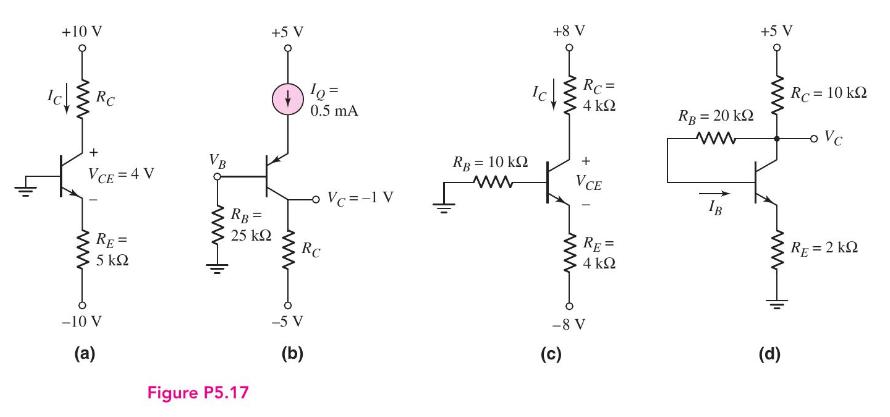
For all the transistors in Figure P5.17, \(\beta=75\). The results of some measurements are indicated on the figures. Find the values of the other labeled currents, voltages, and/or resistor values. +10 V www RC + VB VCE=4 V RE= 5 RB= 25 +5 V www -10 V (a) Figure P5.17 -5 V (b) +8 V +5 V 10= 0.5
The emitter resistor values in the circuits show in Figures P5.17(a) and (c) may vary by \(\pm 5\) percent from the given value. Determine the range of calculated parameters. +10 V www RC + VB VCE=4 V RE= 5 RB= 25 +5 V www -10 V (a) Figure P5.17 -5 V (b) +8 V +5 V 10= 0.5 mA 1c RC= Rc = 10 k 4
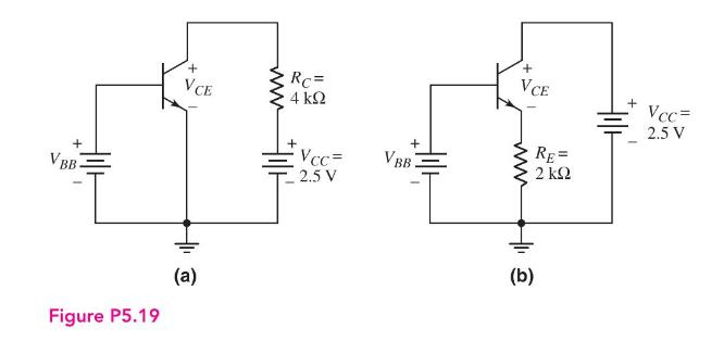
Consider the two circuits in Figure P5.19. The parameters of each transistor are \(I_{S}=5 \times 10^{-16} \mathrm{~A}\) and \(\beta=90\). Determine \(V_{B B}\) in each circuit such that \(V_{C E}=1.10 \mathrm{~V}\) VBB + VCE Figure P5.19 (a) www Rc= 4 Vcc= 2.5 V VBB + VCE www + Vcc= RE= 2 2.5 V
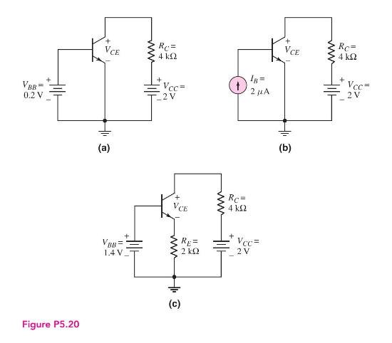
The current gain for each transistor in the circuits shown in Figure P5.20 is \(\beta=120\). For each circuit, determine \(I_{C}\) and \(V_{C E}\). VBB= 0.2 V Figure P5.20 VCE Rc= 4 (a) VBB= 1.4 V 48= Vcc= 2A 2 V + VCE www + www RC= 4 RE= 2 Vcc= 2 V + VCE H (b) www Rc= 4 Vcc= 2 V
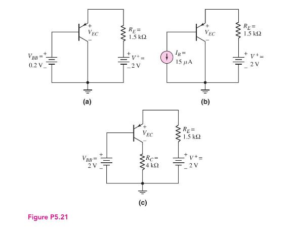
Consider the circuits in Figure P5.21. For each transistor, \(\beta=120\). Determine \(I_{C}\) and \(V_{E C}\) for each circuit. VBB= 0.2 V VEC VBB= 2 V www RE= 1.5 18= V+= 15 A 2 V www Figure P5.21 (c) VEC www RE= 1.5 k2. RC= 4 V+= 2 V H VEC (b) www RE= 1.5 V+= 2 V
(a) The circuit and transistor parameters for the circuit shown in Figure 5.20(a) are \(V_{C C}=3 \mathrm{~V}, V_{B B}=1.3 \mathrm{~V}\), and \(\beta=100\). Redesign the circuit such that \(I_{B Q}=5 \mu \mathrm{A}\) and \(V_{C E Q}=1.5 \mathrm{~V}\).(b) Using the results of part (a), determine the
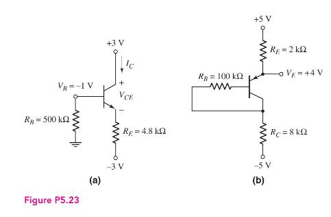
In the circuits shown in Figure P5.23, the values of measured parameters are shown. Determine \(\beta, \alpha\), and the other labeled currents and voltages. Sketch the dc load line and plot the \(Q\)-point. RR = 500 k VB=-1 V ww Figure P5.23 (a) +3 V -3 V + VCE RE = 4.8 +5 V RB = 100 k ww RE=2 k
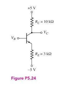
(a) For the circuit in Figure P5.24, determine \(V_{B}\) and \(I_{E}\) such that \(V_{B}=V_{C}\). Assume \(\beta=90\). (b) What value of \(V_{B}\) results in \(V_{C E}=2 \mathrm{~V}\) ? VB +5 V -5 V Figure P5.24 Rc = 10 kQ Vc RE=3 kQ
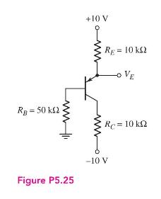
(a) The bias voltages in the circuit shown in Figure P5.25 are changed to \(V^{+}=3.3 \mathrm{~V}\) and \(V^{-}=-3.3 \mathrm{~V}\). The measured value of emitter voltage is \(V_{E}=0.85 \mathrm{~V}\). Determine \(I_{E}, I_{C}, \beta, \alpha\), and \(V_{E C}\). (b) Using the results of part (a),
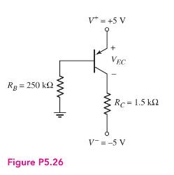
The transistor shown in Figure P5.26 has \(\beta=120\). Determine \(I_{C}\) and \(V_{E C}\). Plot the load line and the \(Q\)-point. V = +5 V RB = 250 k + VEC Rc 1.5 ks2 Figure P5.26 V-=-5 V
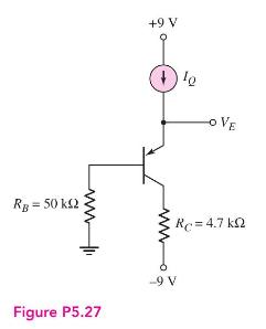
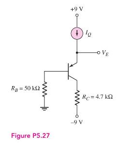
The transistor in the circuit shown in Figure P5.27 is biased with a constant current in the emitter. If \(I_{Q}=1 \mathrm{~mA}\), determine \(V_{C}\) and \(V_{E}\). Assume \(\beta=50\). +9 V -OVE RB = 50 k2 Rc 4.7 k Figure P5.27 -9 V
In the circuit in Figure P5.27, the constant current is \(I=0.5 \mathrm{~mA}\). If \(\beta=50\), determine the power dissipated in the transistor. Does the constant current source supply or dissipate power? What is the value? RB = 50 k2 +9 V Figure P5.27 -9 V -OVE Rc-4.7 k
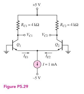
For the circuit shown in Figure P5.29, if \(\beta=200\) for each transistor, determine: (a) \(I_{E 1}\), (b) \(I_{E 2}\), (c) \(V_{C 1}\), and (d) \(V_{C 2}\). +5 V RC = 4 ks Rc2=4 ks2 -o VCL Vc2 Q2 IEL 1E2 Figure P5.29 -5 V 1=1 mA
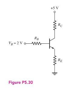
The circuit shown in Figure P5.30 is to be designed such that \(I_{C Q}=0.8 \mathrm{~mA}\) and \(V_{C E Q}=2 \mathrm{~V}\) for the case when (a) \(R_{E}=0\) and (b) \(R_{E}=1 \mathrm{k} \Omega\). Assume \(\beta=80\). (c) The transistor in Figure P5.30 is replaced with one with a value of
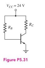
(a) The bias voltage in the circuit in Figure P5.31 is changed to \(V_{C C}=9 \mathrm{~V}\). The transistor current gain is \(\beta=80\). Design the circuit such that \(I_{C Q}=0.25 \mathrm{~mA}\) and \(V_{C E Q}=4.5 \mathrm{~V}\).(b) If the transistor is replaced by a new one with \(\beta=120\),
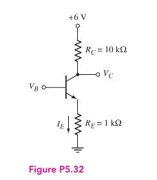
The current gain of the transistor in the circuit shown in Figure P5.32 is \(\beta=150\). Determine \(I_{C}, I_{E}\), and \(V_{C}\) for (a) \(V_{B}=0.2 \mathrm{~V}\), (b) \(V_{B}=0.9 \mathrm{~V}\), (c) \(V_{B}=1.5 \mathrm{~V}\), and (d) \(V_{B}=2.2 \mathrm{~V}\). VBO +6 V Figure P5.32 Rc = 10 kQ Vc
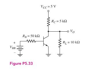
(a) The current gain of the transistor in Figure P5.33 is \(\beta=75\). Determine \(V_{O}\) for: (i) \(V_{B B}=0\), (ii) \(V_{B B}=1 \mathrm{~V}\), and (iii) \(V_{B B}=2 \mathrm{~V}\).(b) Verify the results of part (a) with a computer simulation. VBB = 50 ww Figure P5.33 Vcc=5V Rc=5 k Vo R = 10 kQ
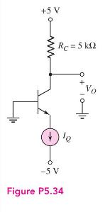
(a) The transistor shown in Figure \(\mathrm{P} 5.34\) has \(\beta=100\). Determine \(V_{O}\) for (i) \(I_{Q}=0.1 \mathrm{~mA}\), (ii) \(I_{Q}=0.5 \mathrm{~mA}\), and (iii) \(I_{Q}=2 \mathrm{~mA}\).(b) Determine the percent change in \(V_{O}\) for the conditions in part (a) if the current gain
Assume \(\beta=120\) for the transistor in the circuit shown in Figure P5.34. Determine \(I_{Q}\) such that (a) \(V_{O}=4 \mathrm{~V}\), (b) \(V_{O}=2 \mathrm{~V}\), and (c) \(V_{O}=0\). +5 V Rc=5kQ -5 V Figure P5.34 10
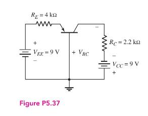
For the circuit shown in Figure P5.27, calculate and plot the power dissipated in the transistor for \(I_{Q}=0,0.5,1.0,1.5,2.0,2.5\), and \(3.0 \mathrm{~mA}\). Assume \(\beta=50\). RE=4kQ ww + VEE=9V + VBC Rc=2.2 kn Figure P5.37 Vcc=9V
Consider the common-base circuit shown in Figure P5.37. Assume the transistor alpha is \(\alpha=0.9920\). Determine \(I_{E}, I_{C}\), and \(V_{B C}\). RE=4kQ ww + VEE=9V + VBC Rc=2.2 kn Figure P5.37 Vcc=9V
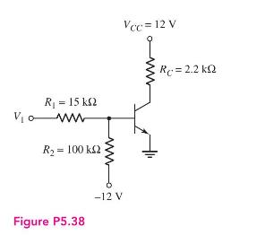
(a) For the transistor in Figure P5.38, \(\beta=80\). Determine \(V_{1}\) such that \(V_{C E Q}=6 \mathrm{~V}\). (b) Determine the range in \(V_{1}\) that produces \(3 \leq V_{C E Q} \leq 9 \mathrm{~V}\). R = 15 ks Vo ww R = 100 k2 Figure P5.38 -12 V Vcc 12 V Rc = 2.2 kQ K
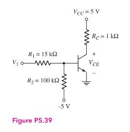
Let \(\beta=25\) for the transistor in the circuit shown in Figure P5.39. Determine the range of \(V_{1}\) such that \(1.0 \leq V_{C E} \leq 4.5\mathrm{~V}\). Sketch the load line and show the range of the \(Q\)-point values. R = 15kQ Vcc 5 V RC=1 k + R = 100 k VCE Figure P5.39 -5 V
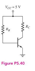
(a) The circuit shown in Figure P5.40 is to be designed such that \(I_{C Q}=\) \(0.5 \mathrm{~mA}\) and \(V_{C E Q}=2.5 \mathrm{~V}\). Assume \(\beta=120\). Sketch the load line and plot the \(Q\)-point. (b) Pick standard values of resistors that are close to the designed values. Assume that the
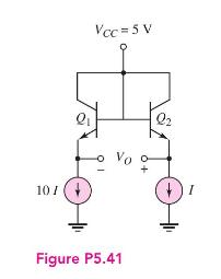
The circuit shown in Figure P5.41 is sometimes used as a thermometer. Assume the transistors \(Q_{1}\) and \(Q_{2}\) in the circuit are identical. Writing the emitter currents in the form \(I_{E}=I_{E O} \exp \left(V_{B E} / V_{T}\right)\), derive the expression for the output voltage \(V_{O}\) as
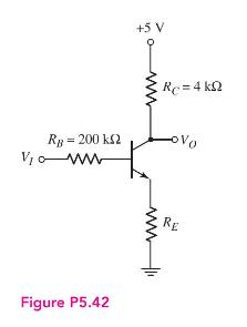
The transistor in Figure P5.42 has \(\beta=120\).(a) Determine \(V_{I}\) that produces \(V_{O}=4 \mathrm{~V}\) for (i) \(R_{E}=0\) and (ii) \(R_{E}=1 \mathrm{k} \Omega\).(b) Repeat part (a) for \(V_{O}=2.5 \mathrm{~V}\).(c) Determine \(V_{O}\) for \(V_{I}=3.5 \mathrm{~V}\) and for \(R_{E}=1
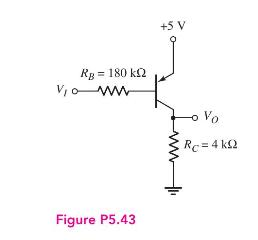
The common-emitter current gain of the transistor in Figure P5.43 is \(\beta=80\). Plot the voltage transfer characteristics over the range \(0 \leq V_{I} \leq 5 \mathrm{~V}\). RB = 180 k Vo ww Figure P5.43 +5 V - Vo Rc=4kQ
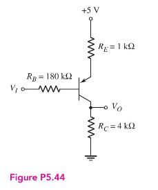
For the circuit shown in Figure P5.44, plot the voltage transfer characteristics over the range \(0 \leq V_{I} \leq 5 \mathrm{~V}\). Assume \(\beta=100\). RB = 180 k2 Figure P5.44 +5 V RE=1 kQ Vo Rc=4kQ
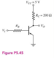
The transistor in the circuit shown in Figure P5.45 has a current gain of \(\beta=40\). Determine \(R_{B}\) such that \(V_{O}=0.2 \mathrm{~V}\) and \(I_{C} / I_{B}=20\) when \(V_{I}=5 \mathrm{~V}\). Vcc 5 V RC=200 $2 Vo RB v, www Figure P5.45
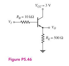
Consider the circuit in Figure P5.46. For the transistor, \(\beta=50\). Find \(I_{B}, I_{C}\), \(I_{E}\), and \(V_{O}\) for (a) \(V_{I}=0\), (b) \(V_{I}=2.5 \mathrm{~V}\), and (c) \(V_{I}=5 \mathrm{~V}\). Rg= 10 k2 Vo ww Vcc=3 V Figure P5.46 ww - Vo RE=500 2
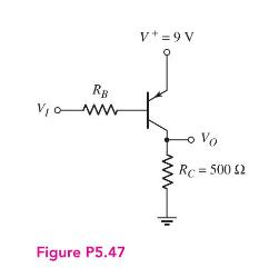
The current gain for the transistor in the circuit in Figure P5.47 is \(\beta=60\). Determine \(R_{B}\) such that \(V_{O}=8.8 \mathrm{~V}\) when \(V_{I}=5 \mathrm{~V}\) and \(I_{C} / I_{B}=25\). RB Vo ww Figure P5.47 V+=9V Vo Rc=500 $2
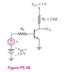
Consider the amplifier circuit shown in Figure P5.48. Assume a transistor current gain of \(\beta=120\). The voltage \(V_{B B}\) establishes the \(Q\)-point, and the voltage \(v_{i}\) is a time-varying signal that produces a variation in the base current, which in turn produces a variation in the
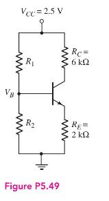
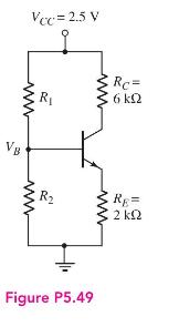
For the transistor in the circuit shown in Figure P5.49, assume \(\beta=120\). Design the circuit such that \(I_{C Q}=0.15 \mathrm{~mA}\) and \(R_{T H}=200 \mathrm{k} \Omega\). What is the value of \(V_{C E Q}\) ? Vcc = 2.5 V R www VB Rc= Figure P5.49 RE= 2 k2
Reconsider Figure P5.49. The transistor current gain is \(\beta=150\). The circuit parameters are changed to \(R_{T H}=120 \mathrm{k} \Omega\) and \(R_{E}=1 \mathrm{k} \Omega\). Determine the values of \(R_{C}, R_{1}\), and \(R_{2}\) such that \(V_{C E Q}=1.5 \mathrm{~V}\) and \(I_{C Q}=0.20
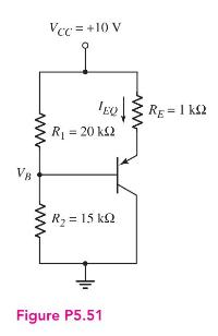
The current gain of the transistor shown in the circuit of Figure P5.51 is \(\beta=100\). Determine \(V_{B}\) and \(I_{E Q}\). VB Vcc = +10 V TEQ RE = 1 k R = 20 k2 R = 15 kQ Figure P5.51
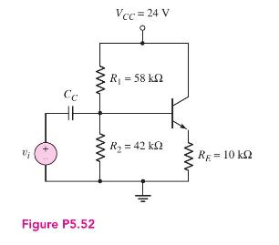
For the circuit shown in Figure P5.52, let \(\beta=125\). (a) Find \(I_{C Q}\) and \(V_{C E Q}\). Sketch the load line and plot the \(Q\)-point. (b) If the resistors \(R_{1}\) and \(R_{2}\) vary by \(\pm 5\) percent, determine the range in \(I_{C Q}\) and \(V_{C E Q}\). Plot the various
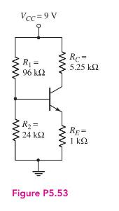
Consider the circuit shown in Figure P5.53. (a) Determine \(I_{B Q}, I_{C Q}\), and \(V_{C E Q}\) for \(\beta=80\). (b) What is the percent change in \(I_{C Q}\) and \(V_{C E Q}\) if \(\beta\) is changed to \(\beta=120\) ? Vcc=9V R = 96 k2 Rc= 15.25 R = RE= 24 Figure P5.53
(a) Redesign the circuit shown in Figure P5.49 using \(V_{C C}=9 \mathrm{~V}\) such that the voltage drop across \(R_{C}\) is \(\left(\frac{1}{3}\right) V_{C C}\) and the voltage drop across \(R_{E}\) is \(\left(\frac{1}{3}\right) V_{C C}\). Assume \(\beta=100\). The quiescent collector current is
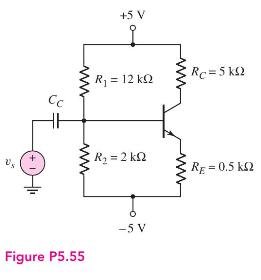
For the circuit shown in Figure P5.55, let \(\beta=100\). (a) Find \(R_{T H}\) and \(V_{T H}\) for the base circuit. (b) Determine \(I_{C Q}\) and \(V_{C E Q}\). (c) Draw the load line and plot the \(Q\)-point. (d) If the resistors \(R_{C}\) and \(R_{E}\) vary by \(\pm 5\) percent, determine the
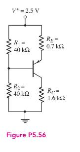
Consider the circuit shown in Figure P5.56. (a) Determine \(R_{T H}, V_{T H}, I_{B Q}\), \(I_{C Q}\), and \(V_{E C Q}\) for \(\beta=90\). (b) Determine the percent change in \(I_{C Q}\) and \(V_{E C Q}\) if \(\beta\) is changed to \(\beta=150\). V+= 2.5 V ww R = 40 R = 40 RE= 0.7 Rc= 1.6 ww
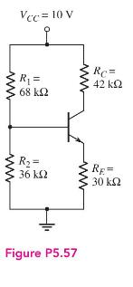
(a) Determine the \(Q\)-point values for the circuit in Figure P5.57. Assume \(\beta=50\).(b) Repeat part (a) if all resistor values are reduced by a factor of 3 .(c) Sketch the load lines and plot the \(Q\)-point values for parts (a) and (b). www Vcc = 10 V R = 68 RC= 42 R= 36 Figure P5.57 RE=
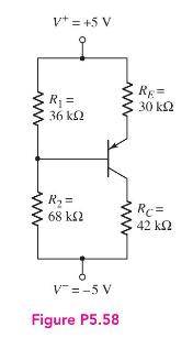
(a) Determine the \(Q\)-point values for the circuit in Figure P5.58. Assume \(\beta=50\).(b) Repeat part (a) if all resistor values are reduced by a factor of 3.(c) Sketch the load lines and plot the \(Q\)-point values for parts (a) and (b). V+=+5 V www R = 36 RR= 30 R = 68 RC= 42 V=-5 V
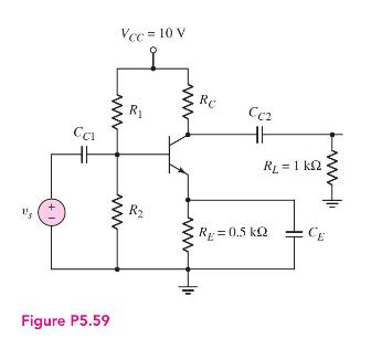
(a) For the circuit shown in Figure P5.59, design a bias-stable circuit such that \(I_{C Q}=0.8 \mathrm{~mA}\) and \(V_{C E Q}=5 \mathrm{~V}\). Let \(\beta=100\).(b) Using the results of part (a), determine the percentage change in \(I_{C Q}\) if \(\beta\) is in the range \(75 \leq \beta \leq
Showing 1200 - 1300
of 4723
First
6
7
8
9
10
11
12
13
14
15
16
17
18
19
20
Last
Step by Step Answers