New Semester
Started
Get
50% OFF
Study Help!
--h --m --s
Claim Now
Question Answers
Textbooks
Find textbooks, questions and answers
Oops, something went wrong!
Change your search query and then try again
S
Books
FREE
Study Help
Expert Questions
Accounting
General Management
Mathematics
Finance
Organizational Behaviour
Law
Physics
Operating System
Management Leadership
Sociology
Programming
Marketing
Database
Computer Network
Economics
Textbooks Solutions
Accounting
Managerial Accounting
Management Leadership
Cost Accounting
Statistics
Business Law
Corporate Finance
Finance
Economics
Auditing
Tutors
Online Tutors
Find a Tutor
Hire a Tutor
Become a Tutor
AI Tutor
AI Study Planner
NEW
Sell Books
Search
Search
Sign In
Register
study help
computer science
systems analysis and design 12th
Microelectronics Circuit Analysis And Design 4th Edition Donald A. Neamen - Solutions
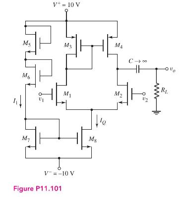
Consider the circuit in Figure P11.101. Use standard transistors. Using a computer simulation, determine the small-signal differential-mode voltage gain and common-mode voltage gain for (a) \(R_{L}=10 \mathrm{M} \Omega\) and (b) \(R_{L}=200 \mathrm{k} \Omega\). V+= 10 V Ms M3 MA C M6 T M1 M2 M Ms
Design a basic BJT diff-amp with an active load and constant currentsource biasing. The bias voltages are to be \(\pm 3 \mathrm{~V}\) and the maximum power dissipation is to be limited to \(2 \mathrm{~mW}\). The open-circuit differential-mode voltage gain should be \(\left|A_{d}\right|=1800\) and
Design a basic MOSFET diff-amp with an active load and constant current-source biasing. The bias voltages are to be \(\pm 3 \mathrm{~V}\) and the maximum power dissipation is to be limited to \(2 \mathrm{~mW}\). The open-circuit differentialmode voltage gain should be \(\left|A_{d}\right|=180\) and
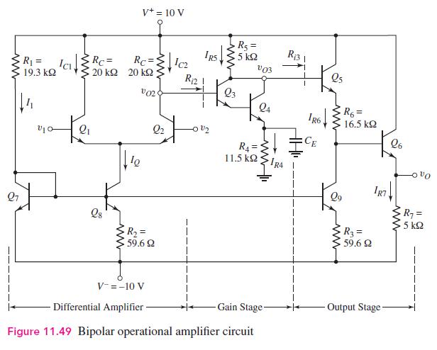
Consider the bipolar op-amp configuration in Figure 11.49. The bias voltages are \(\pm 10 \mathrm{~V}\), as shown, the current \(I_{R 7}\) is to be \(I_{R 7}=3 \mathrm{~mA}\), and the maximum dc power dissipation in the circuit is to be \(120 \mathrm{~mW}\). The output voltage is to be \(v_{o}=0\)
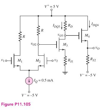
The transistor parameters for the circuit in Figure P11.105 are: \(K_{n}=\) \(0.2 \mathrm{~mA} / \mathrm{V}^{2}, V_{T N}=0.8 \mathrm{~V}\), and \(\lambda=0\). The output resistance of the constant-current source is \(R_{o}=100 \mathrm{k} \Omega\). (a) For \(v_{1}=v_{2}=0\), design the circuit such
What are the two general types of feedback and what are the advantages and disadvantages of each type?
Write the ideal form of the general feedback transfer function.
Define the loop gain factor.
What is the difference between open-loop gain and closed-loop gain?
Describe what is meant by the terms (a) gain sensitivity and (b) bandwidth extension.
Describe the series and shunt input connections of a feedback amplifier.
Describe the series and shunt output connections of a feedback amplifier.
Describe the effect of a series or shunt input connection on the value of input resistance.
Describe the effect of a series or shunt output connection on the value of output resistance.
Consider a noninverting op-amp circuit. Describe the type of input and output feedback connections.
Consider an inverting op-amp circuit. Describe the type of input and output feedback connections.
What is the Nyquist stability criterion for a feedback amplifier?
Using Bode plots, describe the conditions of stability and instability in a feedback amplifier.
What is meant by frequency compensation?
What is a dominant pole?
What is a common technique of frequency compensation in a feedback amplifier?
Sketch the basic BJT two-transistor current source and explain the operation.
Explain the significance of the output resistance of the current-source circuit.
Discuss the effect of mismatched transistors on the characteristics of the BJT two-transistor current source.
Sketch the BJT three-transistor current source and discuss the advantages of this circuit.
What is the primary advantage of a BJT cascode current source?
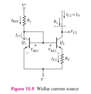
Sketch a Widlar current source and explain the operation.
Can a piecewise linear model of the transistor be used in the analysis of the Widlar current source? Why or why not?
Discuss the operation and significance of a multiple-output transistor current mirror.
Sketch the basic MOSFET two-transistor current source and explain the operation.
Discuss the effect of mismatched transistors on the characteristics of the MOSFET two-transistor current source.
Discuss how the reference portion of a MOSFET current source can be designed with MOSFETs only.
Sketch a MOSFET cascode current source circuit and discuss the advantages of this design.
Discuss the operation of an active load.
What is the primary advantage of using an active load?
Sketch the voltage transfer characteristics of a simple amplifier with an active load. Where should the \(Q\)-point be placed?
What is the impedance seen looking into a simple active load?
What is the advantage of using a cascode active load?
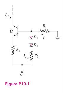
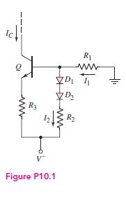
Figure P10.1 shows another form of a bipolar current source.(a) Neglecting base currents, derive the expression for \(I_{C}\) in terms of the circuit, transistor, and diode parameters.(b) If the transistor \(\mathrm{B}-\mathrm{E}\) and diode voltages are equal, show that, for \(R_{1}=R_{2}\), the
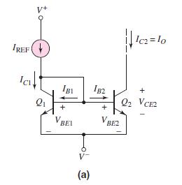
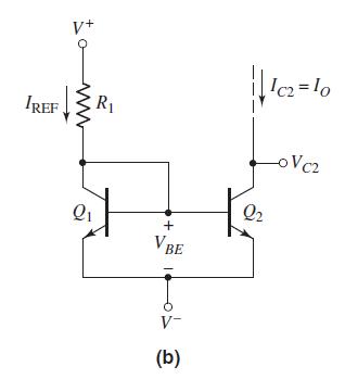
The matched transistors \(Q_{1}\) and \(Q_{2}\) in Figure 10.2 (a) have parameters \(I_{S}=10^{-16} \mathrm{~A}\).(a) For \(\beta=\infty\), determine \(I_{O}\) and \(V_{B E 1}\) for (i) \(I_{\mathrm{REF}}=50 \mu \mathrm{A}\), (ii) \(I_{\mathrm{REF}}=150 \mu \mathrm{A}\), and (iii)
Consider the circuit in Figure 10.2(a). Let \(I_{\mathrm{REF}}=200 \mu \mathrm{A}\). Assume transistor parameters of \(\beta=80, I_{S 1}=5 \times 10^{-15} \mathrm{~A}\), and \(I_{S 2}=2 \times 10^{-15} \mathrm{~A}\). Find \(V_{B E 1}, V_{B E 2}\), and \(I_{O}\).Figure 10.2(a):- IREF V+ Ic2=10 IBI +
Reconsider the circuit in Figure 10.2(a). Let \(I_{\text {REF }}=150 \mu \mathrm{A}\). Assume transistor parameters of \(\beta=120, I_{S 1}=10^{-16} \mathrm{~A}\), and \(I_{S 2}=3 \times 10^{-16} \mathrm{~A}\). Find\(V_{B E 1}, V_{B E 2}\), and \(I_{O}\).Figure 10.2(a):- ww R www 'a R3 D Figure
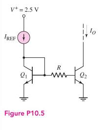
Consider the circuit shown in Figure P10.5. Assume \(I_{\mathrm{REF}}=200 \mu \mathrm{A}\) and \(R=2 \mathrm{k} \Omega\). The transistor parameters are \(\beta=40, I_{S 1}=I_{S 2}=5 \times 10^{-15} \mathrm{~A}\). Find \(V_{B E 1}, V_{B E 2}\), and \(I_{O}\). V+= 2.5 V IREF Figure P10.5 R www Q2
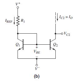
The transistor and circuit parameters for the circuit in Figure 10.2 (b) are: \(V_{B E}\) (on) \(=0.7 \mathrm{~V}, \beta=60, V_{A}=\infty, V^{+}=+3 \mathrm{~V}, V^{-}=-3 \mathrm{~V}\), and \(I_{\mathrm{REF}}=\) \(0.250 \mathrm{~mA}\). Determine the value of \(R_{1}\) and determine \(I_{C 1}, I_{B
The bias voltages in the circuit shown in Figure 10.2(b) are \(V^{+}=+5 \mathrm{~V}\), \(V^{-}=-5 \mathrm{~V}\) and the resistor value is \(R_{1}=18.3 \mathrm{k} \Omega\). Assume transistor parameters of \(V_{B E}\) (on) \(=0.7 \mathrm{~V}, \beta=80\), and \(V_{A}=\infty\). Determine
Consider the current source in Figure 10.2(b). The circuit is biased at \(V^{+}=2.5 \mathrm{~V}\) and \(V^{-}=-2.5 \mathrm{~V}\). The transistor parameters are \(\beta \cong \infty\), \(V_{A}=\infty\), and \(I_{S 2}=10^{-15} \mathrm{~A}\). The circuit is to be designed such that \(I_{O}=0.25
For the basic two-transistor current source in Figure 10.2(b), the transistor parameters are: \(\beta=120, V_{B E}(\) on \()=0.7 \mathrm{~V}\), and \(V_{A}=100 \mathrm{~V}\). The bias voltages are \(V^{+}=5 \mathrm{~V}\) and \(V^{-}=-5 \mathrm{~V}\). (a) Design the circuit such that \(I_{O}=0.5
The transistors in the basic current mirror in Figure 10.2(b) have a finite \(\beta\) and an infinite Early voltage. The B-E area of \(Q_{2}\) is \(n\) times that of \(Q_{1}\). Derive the expression for \(I_{O}\) in terms of \(I_{\mathrm{REF}}, \beta\), and \(n\).Figure 10.2(b):- IREF V+ ww R + VBE
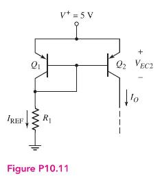
Figure P10.11 shows a basic two-transistor pnp current source. The transistor parameters are \(V_{E B}(\mathrm{on})=0.7 \mathrm{~V}, \beta=40\), and \(V_{A}=\infty\). Design the circuit such that \(I_{O}=0.20 \mathrm{~mA}\) and determine the value of \(I_{\mathrm{REF}}\). IREF www V+= 5 V R Figure
In the circuit in Figure P10.11, the transistor parameters are \(\beta=80\) and \(V_{E B}\) (on) \(=0.7 \mathrm{~V}\). (a) Design the circuit such that \(I_{O}=120 \mu \mathrm{A}\) for \(V_{E C 2}=\) \(0.7 \mathrm{~V}\). (b) If \(V_{A}=80 \mathrm{~V}\), determine the change in \(I_{O}\) for (i)
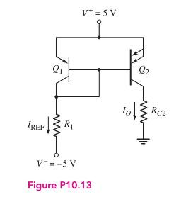
Consider the pnp current source in Figure P10.13, with transistor parameters \(\beta=\infty, V_{A}=\infty\), and \(V_{E B}\) (on) \(=0.7 \mathrm{~V}\). (a) Design the circuit such that \(I_{\mathrm{REF}}=1 \mathrm{~mA}\). (b) What is the value of \(I_{O}\) ? (c) What is the maximum value of \(R_{C
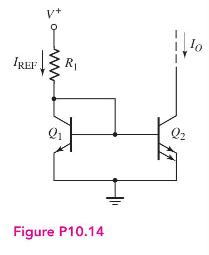
Consider the circuit shown in Figure P10.14. The transistor \(Q_{2}\) is equivalent to two identical transistors in parallel, each of which is matched to \(Q_{1}\). Assume the transistor parameters are \(V_{B E}(\mathrm{on})=0.7 \mathrm{~V}, \beta=60\), and \(V_{A}=\infty\), and assume the bias
Design a basic two-transistor current source circuit configuration such that \(I_{O}=0.40 \mathrm{~mA}\) and \(I_{\mathrm{REF}}=0.20 \mathrm{~mA}\). The circuit is to be biased at \(V^{+}=2.5 \mathrm{~V}\) and \(V^{-}=-2.5 \mathrm{~V}\). Neglect base currents and assume that \(V_{B
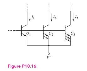
The values of \(\beta\) for the transistors in Figure P10.16 are very large.(a) If \(Q_{1}\) is diode-connected with \(I_{1}=0.5 \mathrm{~mA}\), determine the collector currents in the other two transistors.(b) Repeat part (a) if \(Q_{2}\) is diode-connected with \(I_{2}=0.5 \mathrm{~mA}\).(c)
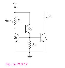
Consider the circuit in Figure P10.17. The transistor parameters are: \(\beta=80\), \(V_{B E}(\mathrm{on})=0.7 \mathrm{~V}\), and \(V_{A}=\infty\). (a) Derive the expression for \(I_{O}\) in terms of \(I_{\mathrm{REF}}, \beta\), and \(R_{2}\). (b) For \(R_{2}=10 \mathrm{k} \Omega\) and \(V^{+}=10
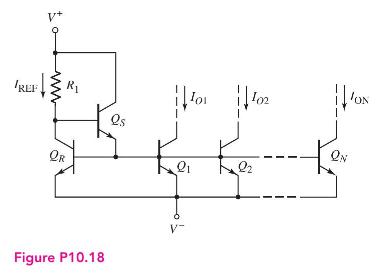
All transistors in the \(N\) output current mirror in Figure P10.18 are matched, with a finite \(\beta\) and \(V_{A}=\infty\). (a) Derive the expression for each load current in terms of \(I_{\text {REF }}\) and \(\beta\). (b) If the circuit parameters are \(V^{+}=5 \mathrm{~V}\) and \(V^{-}=-5\)
Design a pnp version of the basic three-transistor current source circuit, using a resistor to establish \(I_{\mathrm{REF}}\). The bias current is to be \(I_{O}=0.15 \mathrm{~mA}\), and the circuit is to be biased at \(V^{+}=3 \mathrm{~V}\) and \(V^{-}=-3 \mathrm{~V}\). The transistor parameters
Design a pnp version of the Wilson current source, using a resistor to establish \(I_{\text {REFF }}\). The circuit parameters are \(V^{+}=9 \mathrm{~V}\) and \(V^{-}=-9 \mathrm{~V}\), and the transistor parameters are: \(V_{E B}(\) on \()=0.7 \mathrm{~V}, \beta=25\), and \(V_{A}=\infty\). If the
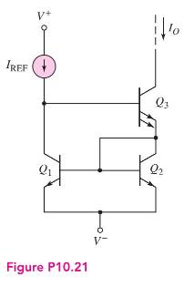
Consider the Wilson current source in Figure P10.21. The transistors have a finite \(\beta\) and an infinite Early voltage. Derive the expression for \(I_{O}\) in terms of \(I_{\text {REF }}\) and \(\beta\). V+ IREF Q3 Q Q2 Figure P10.21 V-
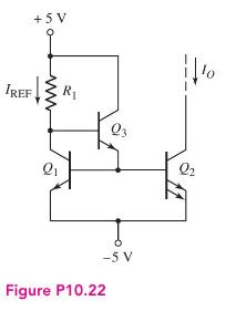
Consider the circuit in Figure P10.22. The transistor parameters for \(Q_{1}\) and \(Q_{2}\) are \(V_{B E 1,2}(\mathrm{on})=0.7 \mathrm{~V}\) and \(\beta_{1,2}=90\). The parameters for \(Q_{3}\) are \(V_{B E 3}(\) on \()=0.6 \mathrm{~V}\) and \(\beta_{3}=60\). Assume \(V_{A}=\infty\) for all
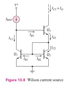
Consider the Wilson current-source circuit shown in Figure 10.8. Assume the reference current is \(0.25 \mathrm{~mA}\) and assume transistor parameters of \(V_{B E}(\) on \()=0.7 \mathrm{~V}, \beta=100\), and \(V_{A}=100 \mathrm{~V}\). (a) Determine the output resistance looking into the collector
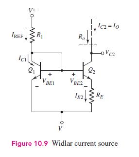
Consider the Widlar current source shown in Figure 10.9. The circuit parameters are \(V^{+}=+5 \mathrm{~V}, V^{-}=0, R_{1}=9.3 \mathrm{k} \Omega\), and \(R_{E}=1.5 \mathrm{k} \Omega\). Assume \(V_{B E 1}=0.7 \mathrm{~V}\). Neglecting base currents, determine \(I_{\mathrm{REF}}, I_{O}\), and \(V_{B
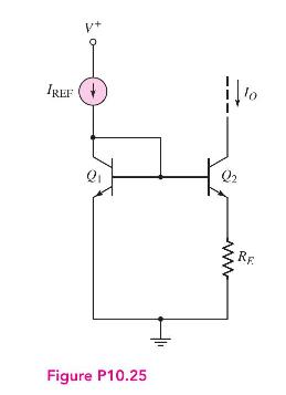
For the circuit shown in Figure P10.25, neglect base currents and assume \(V_{A}=\infty\). Let \(I_{\mathrm{REF}}=200 \mu \mathrm{A}\) and \(R_{E}=500 \Omega\).(a) Assume the transistor parameters are \(I_{S 1}=I_{S 2}=5 \times 10^{-15} \mathrm{~A}\). Find \(V_{B E 1}, V_{B E 2}\), and
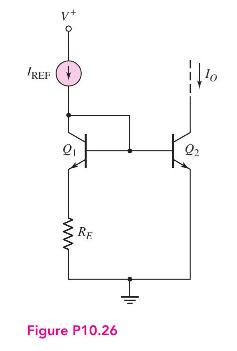
Consider the circuit in Figure P10.26. Neglect base currents and assume \(V_{A}=\infty\). Assume \(I_{\mathrm{REF}}=100 \mu \mathrm{A}\) and \(R_{E}=700 \Omega\).(a) For transistor parameters of \(I_{S 1}=I_{S 2}=5 \times 10^{-15} \mathrm{~A}\), find \(V_{B E 1}, V_{B E 2}\), and \(I_{O}\).(b)
(a) For the Widlar current source shown in Figure 10.9, find \(I_{\text {REF }}, I_{O}\), and \(V_{B E 2}\) if \(R_{1}=50 \mathrm{k} \Omega, R_{E}=3 \mathrm{k} \Omega, V^{+}=5 \mathrm{~V}\), and \(V^{-}=-5 \mathrm{~V}\). The transistor parameters are \(\beta=120\) and \(V_{B E 1}\) (on) \(=0.7
Consider the Widlar current source in Problem 10.27. For \(\beta=80\) and \(V_{A}=80 \mathrm{~V}\), determine the change in \(I_{O}\) corresponding to a \(5 \mathrm{~V}\) change in the output voltage.Data From Problem 10.27:-(a) For the Widlar current source shown in Figure 10.9, find \(I_{\text
(a) Design the Widlar current source such that \(I_{\mathrm{REF}}=0.50 \mathrm{~mA}\) and \(I_{O}=\) \(50 \mu \mathrm{A}\). Assume that \(V^{+}=+5 \mathrm{~V}, V^{-}=-5 \mathrm{~V}, V_{B E 1}=0.7 \mathrm{~V}\), and neglect base currents. (b) If \(\beta=75\) and \(V_{A}=100 \mathrm{~V}\), determine
Design a Widlar current source to provide a bias current of \(I_{O}=50 \mu \mathrm{A}\). The circuit is to be biased at \(V^{+}=3 \mathrm{~V}\) and \(V^{-}=-3 \mathrm{~V}\). Assume \(V_{B E 1}(\) on \()=0.7 \mathrm{~V}\) and \(V_{A}=\infty\). The maximum resistor value is to be limited to \(10
Design the Widlar current source shown in Figure 10.9 such that \(I_{\text {REF }}=\) \(2 \mathrm{~mA}\) and \(I_{O}=50 \mu \mathrm{A}\). Let \(V^{+}=15 \mathrm{~V}\) and \(V^{-}=0\). The transistors are matched, and \(V_{B E}=0.7 \mathrm{~V}\) at \(1 \mathrm{~mA}\). V+ IREF Ici www Q R Ro Ic2=10
The circuit parameters of the Widlar current source in Figure 10.9 are \(V^{+}=3 \mathrm{~V}, V^{-}=-3 \mathrm{~V}\), and \(R_{1}=20 \mathrm{k} \Omega\). Assume \(V_{B E 1}(\mathrm{on})=0.7 \mathrm{~V}\) and \(V_{A}=\infty\). (a) Determine \(I_{\mathrm{REF}}\) and (b) \(R_{E}\) such that
Consider the Widlar current source in Figure 10.9. The circuit parameters are: \(V^{+}=10 \mathrm{~V}, V^{-}=-10 \mathrm{~V}, R_{1}=40 \mathrm{k} \Omega\), and \(R_{E}=12 \mathrm{k} \Omega\). Neglect base currents and assume \(V_{B E 1}=0.7 \mathrm{~V}\) at \(1 \mathrm{~mA}\). Determine
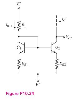
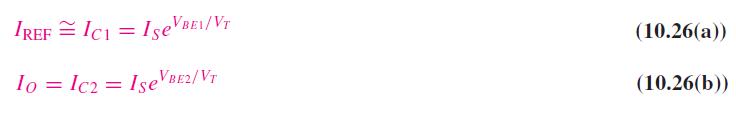
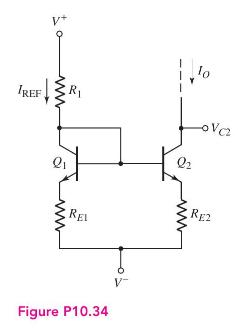
Consider the circuit in Figure P10.34. The transistors are matched. Assume that base currents are negligible and that \(V_{A}=\infty\). Using the current-voltage relationships given by Equations (10.26(a)) and (10.26(b)), show that\[I_{O} R_{E 2}-I_{\mathrm{REF}} R_{E 1}=V_{T} \ln
The modified Widlar current-source circuit shown in Figure P10.34 is biased at \(V^{+}=3 \mathrm{~V}\) and \(V^{-}=-3 \mathrm{~V}\).(a) For \(I_{S 1}=I_{S 2}=10^{-15} \mathrm{~A}\) and \(R_{E 1}=500 \Omega\), design the circuit such that \(I_{\mathrm{REF}}=0.5 \mathrm{~mA}\) and \(I_{O}=0.2
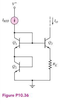
Consider the circuit in Figure P10.36. Neglect base currents and assume \(V_{A}=\infty\). (a) Derive the expression for \(I_{O}\) in terms of \(I_{\text {REF }}\) and \(R_{E}\). (b) Determine the value of \(R_{E}\) such that \(I_{O}=I_{\mathrm{REF}}=100 \mu \mathrm{A}\). Assume \(V_{B E}=0.7
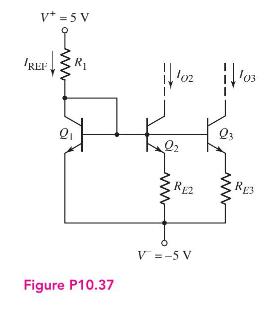
Consider the Widlar current-source circuit with multiple output transistors shown in Figure P10.37. Assume \(V_{B E 1}=0.7\) V. (a) For circuit parameters \(R_{1}=10 \mathrm{k} \Omega, R_{E 2}=1 \mathrm{k} \Omega\), and \(R_{E 2}=2 \mathrm{k} \Omega\), find \(I_{\mathrm{REF}}, I_{O 2}\), and \(I_{O
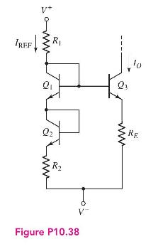
Assume that all transistors in the circuit in Figure P10.38 are matched and that \(\beta=\infty\) (neglect base currents). (a) Derive an expression for \(I_{O}\) in terms of bias voltages and resistor values. (b) Show that if \(R_{1}=R_{2}\) and \(I_{O}=I_{\mathrm{REF}}\), then
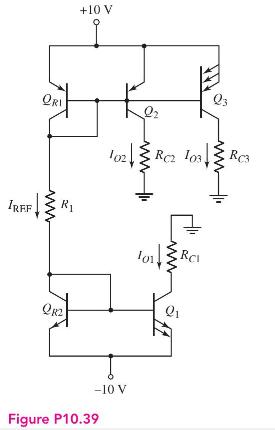
In the circuit in Figure P10.39, the transistor parameters are: \(\beta=\infty\), \(V_{A}=\infty\), and \(V_{B E}=V_{E B}=0.7 \mathrm{~V}\). Let \(R_{C 1}=2 \mathrm{k} \Omega, R_{C 2}=3 \mathrm{k} \Omega, R_{C 3}=\) \(1 \mathrm{k} \Omega\), and \(R_{1}=12 \mathrm{k} \Omega\). (a) Determine \(I_{O
Consider the circuit in Figure P10.39, with transistor parameters \(\beta=\infty\), \(V_{A}=\infty\), and \(V_{B E}\) (on) \(=V_{E B}\) (on) \(=0.7 \mathrm{~V}\). Let \(R_{1}=24 \mathrm{k} \Omega\). (a) Find \(I_{\mathrm{REF}}\), \(I_{O 1}, I_{O 2}\), and \(I_{O 3}\). (b) Determine the maximum
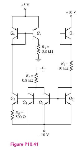
Consider the circuit shown in Figure P10.41. Assume \(V_{B E}=V_{E B}=0.7 \mathrm{~V}\) for all transistors except \(Q_{5}\) and let \(\beta=\infty\). Determine all collector currents, and find \(V_{C E 3}, V_{C E 5}\), and \(V_{E C 7}\). +5 V +10 V Q6 R3 = 0.8 R = ww R = 0.8 10 Qs Q4 RE= 500
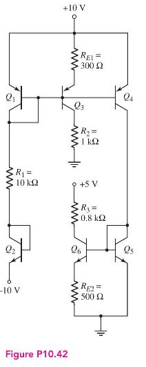
For the circuit shown in Figure P10.42, assume transistor parameters \(V_{B E}=\) \(V_{E B}=0.7 \mathrm{~V}\) for all transistors except \(Q_{3}\) and \(Q_{6}\), and let \(\beta=\infty\). Find the collector current in each transistor. ww R = +10 V REI 300 23 ww R = Q4 10 +5 V R = 10.8 26 Qs -10
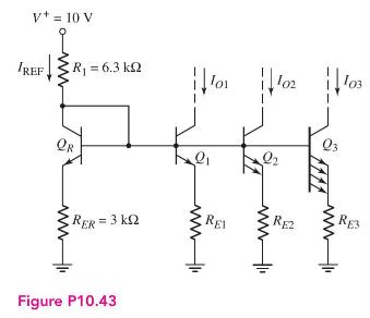
Consider the circuit in Figure P10.43. The transistor parameters are: \(\beta=\infty, V_{A}=\infty\), and \(V_{B E}=0.7 \mathrm{~V}\). Design the circuit such that the B-E voltages of \(Q_{1}, Q_{2}\), and \(Q_{3}\) are identical to that of \(Q_{R}\). What are the values of \(I_{O 1}, I_{O 2}\),
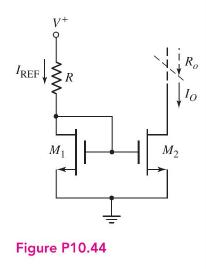
Consider the MOSFET current-source circuit in Figure P10.44 with \(V^{+}=\) \(+2.5 \mathrm{~V}\) and \(R=15 \mathrm{k} \Omega\). The transistor parameters are \(V_{T N}=0.5 \mathrm{~V}, k_{n}^{\prime}=\) \(80 \mu \mathrm{A} / \mathrm{V}^{2}, W / L=6\), and \(\lambda=0\). Determine
The MOSFET current-source circuit in Figure P10.44 is biased at \(V^{+}=\) \(2.0 \mathrm{~V}\). The transistor parameters are \(V_{T N}=0.5 \mathrm{~V}, k_{n}^{\prime}=80 \mu \mathrm{A} / \mathrm{V}^{2}\), and \(\lambda=0.015 \mathrm{~V}^{-1}\). (a) Design the circuit such that
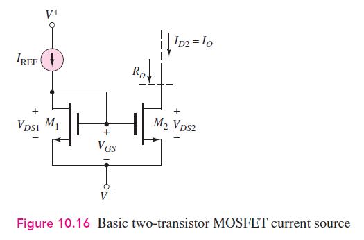
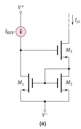
Consider the basic two-transistor NMOS current source in Figure 10.16. The circuit parameters are \(V^{+}=+5 \mathrm{~V}, V^{-}=-5 \mathrm{~V}\), and \(I_{\mathrm{REF}}=250 \mu \mathrm{A}\). The transistor parameters are \(V_{T N}=1 \mathrm{~V}, k_{n}^{\prime}=80 \mu \mathrm{A} / \mathrm{V}^{2}\),
In the two-transistor NMOS current source shown in Figure 10.16, the parameters are: \(V^{+}=3 \mathrm{~V}, V^{-}=-3 \mathrm{~V}\), and \(I_{\mathrm{REF}}=0.2 \mathrm{~mA}\). The transistor parameters are: \(V_{T N 1}=0.4 \mathrm{~V}, K_{n 1}=0.2 \mathrm{~mA} / \mathrm{V}^{2}\), and
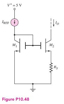
Consider the circuit shown in Figure P10.48. Let \(I_{\text {REF }}=200 \mu\) A. The transistor parameters are \(K_{n 1}=K_{n 2}=0.2 \mathrm{~mA} / \mathrm{V}^{2}, V_{T N 1}=V_{T N 2}=0.5 \mathrm{~V}\), and \(\lambda_{1}=\lambda_{2}=0\). (a) If \(R_{S}=10 \mathrm{k} \Omega\), determine \(I_{O}\)
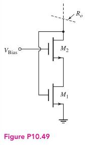
Consider the two-transistor diode-connected circuit in Figure P10.49. Assume that both transistors are biased in the saturation region, and that \(g_{m 1}=g_{m 2} \equiv g_{m}\) and \(r_{o 1}=r_{o 2} \equiv r_{o}\). Neglect the body effect. Derive the expression for the output resistance \(R_{o}\).
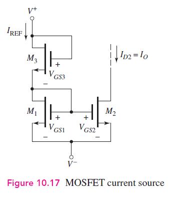
The circuit parameters for the circuit shown in Figure 10.17 are \(V^{+}=1.8 \mathrm{~V}\) and \(V^{-}=-1.8 \mathrm{~V}\). The transistor parameters are \(V_{T N}=0.5 \mathrm{~V}\), \(k_{n}^{\prime}=80 \mu \mathrm{A} / \mathrm{V}^{2}\), and \(\lambda=0\). Design the circuit such that \(I_{O}=0.15
The parameters for the circuit in Figure 10.17 are \(V^{+}=+5 \mathrm{~V}\) and \(V^{-}=0\). The transistor parameters are \(V_{T N}=0.7 \mathrm{~V}, k_{n}^{\prime}=60 \mu \mathrm{A} / \mathrm{V}^{2}\), and \(\lambda=0.015 \mathrm{~V}^{-1}\). The transistor width-to-length ratios are \((W /
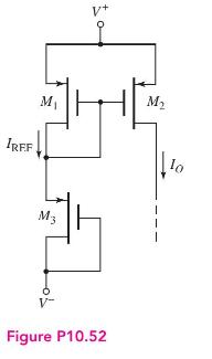
Figure P10.52 is a PMOS version of the current-source circuit shown in Figure 10.17. The transistor \(M_{2}\) sources a bias current to a load circuit. Assume the circuit is biased at \(V^{+}=+5 \mathrm{~V}\) and \(V^{-}=-5 \mathrm{~V}\), and assume the transistor parameters are \(V_{T P}=-0.5
The circuit shown in Figure P10.52 is biased at \(V^{+}=+2 \mathrm{~V}\) and \(V^{-}=\) \(-2 \mathrm{~V}\). Assume the transistor parameters are \(V_{T P}=-0.35 \mathrm{~V}, k_{p}^{\prime}=\) \(50 \mu \mathrm{A} / \mathrm{V}^{2}\), and \(\lambda=0\). Design the circuit such that
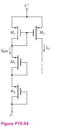
The transistor circuit shown in Figure P10.54 is biased at \(V^{+}=+5 \mathrm{~V}\) and \(V^{-}=-5 \mathrm{~V}\). The transistor parameters are \(V_{T P}=-1.2 \mathrm{~V}, k_{p}^{\prime}=\) \(80 \mu \mathrm{A} / \mathrm{V}^{2}, \lambda=0,(W / L)_{1}=(W / L)_{2}=25\), and \((W / L)_{3}=(W /
Assume the circuit shown in Figure P10.54 is biased at \(V^{+}=3 \mathrm{~V}\) and \(V^{-}=-3 \mathrm{~V}\). The transistor parameters are \(V_{T P}=-0.5 \mathrm{~V}, k_{p}^{\prime}=60 \mu \mathrm{A} / \mathrm{V}^{2}\), and \(\lambda=0\). Design the circuit such that \(I_{\mathrm{REF}}=250 \mu
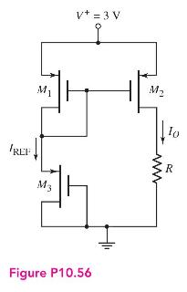
The circuit in Figure P10.56 is a PMOS version of a two-transistor MOS current mirror. Assume transistor parameters of \(V_{T P}=-0.4 \mathrm{~V}\), \(k_{p}^{\prime}=60 \mu \mathrm{A} / \mathrm{V}^{2}\), and \(\lambda=0\). The transistor width-to-length ratios are \((W / L)_{1}=25,(W / L)_{2}=15\),
The transistors in Figure P10.56 have the same parameters as in Problem 10.56 except for the \(W / L\) ratios. Design the circuit such that \(I_{O}=80 \mu \mathrm{A}\), \(I_{\mathrm{REF}}=220 \mu \mathrm{A}\), and \(V_{S D 2}(\mathrm{sat})=0.35 \mathrm{~V}\). V+= 3 V M M2 To 'REF M3 R Figure P10.56
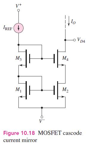
Consider the NMOS cascode current source in Figure 10.18. The circuit parameters are \(V^{+}=5 \mathrm{~V}, V^{-}=-5 \mathrm{~V}\), and \(I_{\mathrm{REF}}=100 \mu \mathrm{A}\). All transistors are matched with parameters \(V_{T N}=0.5 \mathrm{~V}, K_{n}=100 \mu \mathrm{A} / \mathrm{V}^{2}\), and
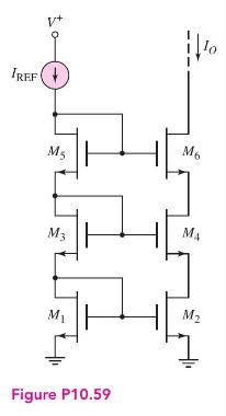
Consider the NMOS current source in Figure P10.59. Let \(I_{\mathrm{REF}}=0.2 \mathrm{~mA}\), \(K_{n}=0.2 \mathrm{~mA} / \mathrm{V}^{2}, V_{T N}=1 \mathrm{~V}\), and \(\lambda=0.02 \mathrm{~V}^{-1}\). (All transistors are matched.) Determine the output resistance looking into the drain of
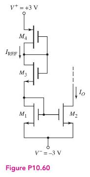
The transistors in the circuit shown in Figure P10.60 have parameters \(V_{T N}=0.4 \mathrm{~V}, \quad V_{T P}=-0.4 \mathrm{~V}, \quad k_{n}^{\prime}=100 \mu \mathrm{A} / \mathrm{V}^{2}, k_{p}^{\prime}=60 \mu \mathrm{A} / \mathrm{V}^{2}\), and \(\lambda_{n}=\lambda_{p}=0\). The transistor
The transistors in the circuit shown in Figure P10.60 have the same parameters as in Problem 10.60 except for the \((W / L)\) ratios. Design the circuit such that \(I_{O}=50 \mu \mathrm{A}, I_{\mathrm{REF}}=500 \mu \mathrm{A}, V_{D S 2}(\mathrm{sat})=0.5 \mathrm{~V}\), and \(V_{G S 3}=V_{S G
A Wilson current mirror is shown in Figure 10.20(a). The parameters are: \(V^{+}=5 \mathrm{~V}, V^{-}=-5 \mathrm{~V}\), and \(I_{\text {REF }}=80 \mu \mathrm{A}\). The transistor parameters are: \(V_{T N}=1 \mathrm{~V}, K_{n}=80 \mu \mathrm{A} / \mathrm{V}^{2}\), and \(\lambda=0.02
Showing 700 - 800
of 4723
1
2
3
4
5
6
7
8
9
10
11
12
13
14
15
Last
Step by Step Answers