New Semester
Started
Get
50% OFF
Study Help!
--h --m --s
Claim Now
Question Answers
Textbooks
Find textbooks, questions and answers
Oops, something went wrong!
Change your search query and then try again
S
Books
FREE
Study Help
Expert Questions
Accounting
General Management
Mathematics
Finance
Organizational Behaviour
Law
Physics
Operating System
Management Leadership
Sociology
Programming
Marketing
Database
Computer Network
Economics
Textbooks Solutions
Accounting
Managerial Accounting
Management Leadership
Cost Accounting
Statistics
Business Law
Corporate Finance
Finance
Economics
Auditing
Tutors
Online Tutors
Find a Tutor
Hire a Tutor
Become a Tutor
AI Tutor
AI Study Planner
NEW
Sell Books
Search
Search
Sign In
Register
study help
computer science
systems analysis and design 12th
Microelectronics Circuit Analysis And Design 4th Edition Donald A. Neamen - Solutions
A car's radio may be subjected to voltage spikes induced by coupling from the ignition system. Pulses on the order of \(\pm 250 \mathrm{~V}\) and lasting for \(120 \mu \mathrm{s}\) may exist. Design a clipper circuit using resistors, diodes, and Zener diodes to limit the input voltage between \(+14
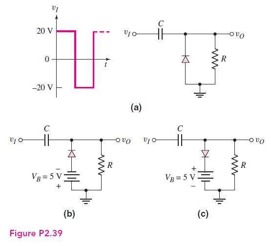
For the circuit in Figure P2.39(b), let \(V_{\gamma}=0\) and \(v_{I}=10 \sin \omega t(\mathrm{~V})\). Plot \(v_{O}\) versus time over three cycles of input voltage. Assume the initial voltage across the capacitor is zero and assume the \(R C\) time constant is very large.Figure P2.39:- 20 V VI C HH
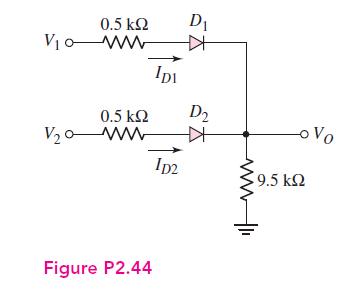
The diodes in the circuit in Figure P2.44 have piecewise linear parameters of \(V_{\gamma}=0.6 \mathrm{~V}\) and \(r_{f}=0\). Determine the output voltage \(V_{O}\) and the diode currents \(I_{D 1}\) and \(I_{D 2}\) for the following input conditions:(a) \(V_{1}=10 \mathrm{~V}\), \(V_{2}=0\);(b)
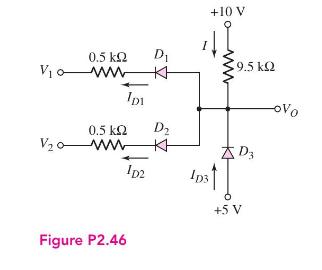
The diodes in the circuit in Figure P2.46 have the same piecewise linear parameters as described in Problem 2.44. Determine the output voltage \(V_{O}\) and the currents \(I_{D 1}, I_{D 2}, I_{D 3}\), and \(I\) for the following input conditions:(a) \(V_{1}=V_{2}=0\);(b) \(V_{1}=V_{2}=5
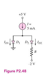
The diode cut-in voltage for each diode in the circuit shown in Figure P2.48 is \(0.7 \mathrm{~V}\). Determine the value of \(R\) such that (a) \(I_{D 1}=I_{D 2}\), (b) \(I_{D 1}=0.2 I_{D 2}\), and (c) \(I_{D 1}=5 I_{D 2}\). +5 V ID D ] = 5 mA D D2 D2 R Figure P2.48 -2 V
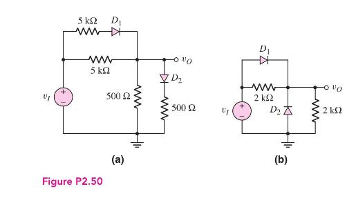
In each circuit shown in Figure P2.50, the diode cut-in voltage is \(V_{\gamma}=0.6 \mathrm{~V}\).(a) For the circuit in Figure P2.50(a), determine \(v_{O}\) for (i) \(v_{I}=+5 \mathrm{~V}\) and (ii) \(v_{I}=-5 \mathrm{~V}\).(b) Repeat part (a) for the circuit in Figure P2.50(b).(c) Plot the
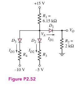
The cut-in voltage of each diode in the circuit shown in Figure P2.52 is \(V_{\gamma}=0.7 \mathrm{~V}\). Determine \(I_{D 1}, I_{D 2}, I_{D 3}\), and \(V_{A}\) for (a) \(R_{3}=14 \mathrm{k} \Omega\), \(R_{4}=24 \mathrm{k} \Omega ;\) (b) \(R_{3}=3.3 \mathrm{k} \Omega, \quad R_{4}=5.2 \mathrm{k}
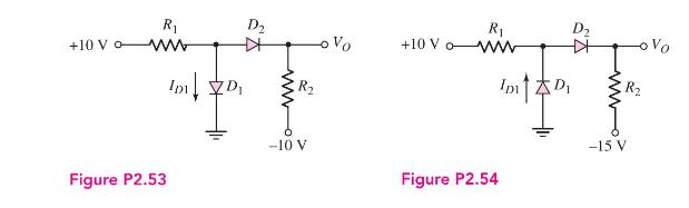
Let \(V_{\gamma}=0.7 \mathrm{~V}\) for each diode in the circuit in Figure P2.53.(a) Find \(I_{D 1}\) and \(V_{O}\) for \(R_{1}=5 \mathrm{k} \Omega\) and \(R_{2}=10 \mathrm{k} \Omega\).(b) Repeat part (a) for \(R_{1}=10 \mathrm{k} \Omega\) and \(R_{2}=5 \mathrm{k} \Omega\). R D R +10 V o www Vo
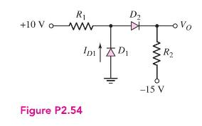
For the circuit shown in Figure P2.54, let \(V_{\gamma}=0.7 \mathrm{~V}\) for each diode. Calculate \(I_{D 1}\) and \(V_{O}\) for (a) \(R_{1}=10 \mathrm{k} \Omega, R_{2}=5 \mathrm{k} \Omega\) and for (b) \(R_{1}=5 \mathrm{k} \Omega\), \(R_{2}=10 \mathrm{k} \Omega\). +10 V R ww D Figure P2.54 -15 V
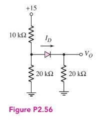
If \(V_{\gamma}=0.7 \mathrm{~V}\) for the diode in the circuit in Figure P2.56 determine \(I_{D}\) and \(V_{O}\). +15 ww 10 -o Vo 20 20 Figure P2.56
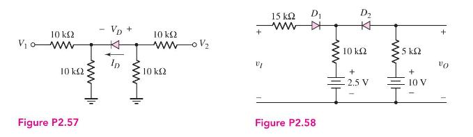
Let \(V_{\gamma}=0.7 \mathrm{~V}\) for the diode in the circuit in Figure P2.57. Determine \(I_{D}\), \(V_{D}, V_{A}\), and \(V_{B}\) for (a) \(V_{1}=V_{2}=6 \mathrm{~V}\); (b) \(V_{1}=2 \mathrm{~V}, V_{2}=5 \mathrm{~V}\); (c) \(V_{1}=5 \mathrm{~V}, V_{2}=4 \mathrm{~V}\); and (d) \(V_{1}=2
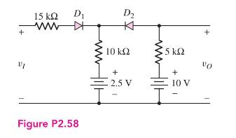
(a) Each diode in the circuit in Figure P2.58 has piecewise linear parameters of \(V_{\gamma}=0\) and \(r_{f}=0\). Plot \(v_{O}\) versus \(v_{I}\) for \(0 \leq v_{I} \leq 30 \mathrm{~V}\). Indicate the breakpoints and give the state of each diode in the various regions of the plot.(b) Compare the
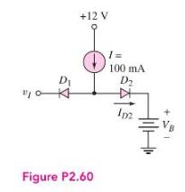
Let \(V_{\gamma}=0.7 \mathrm{~V}\) for each diode in the circuit shown in Figure P2.60. Plot \(I_{D 2}\) versus \(v_{I}\) over the range \(0 \leq v_{I} \leq 12 \mathrm{~V}\) for (a) \(V_{B}=4.5 \mathrm{~V}\) and (b) \(V_{B}=9 \mathrm{~V}\). +12 V D 1= 100 mA. D 102 Figure P2.60
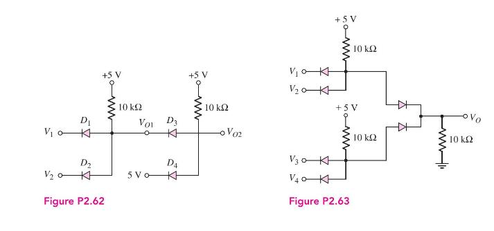
Consider the circuit in Figure P2.62. The output of a diode AND logic gate is connected to the input of a second diode AND logic gate. Assume \(V_{\gamma}=\) \(0.6 \mathrm{~V}\) for each diode. Determine the outputs \(V_{O 1}\) and \(V_{O 2}\) for: (a) \(V_{1}=\) \(V_{2}=5 \mathrm{~V}\); (b)
Consider the circuit shown in Figure P2.64. The forward-bias cut-in voltage of the diode is \(1.5 \mathrm{~V}\) and the forward-bias resistance is \(r_{f}=10 \Omega\). Determine the value of \(R\) required to limit the current to \(I=12 \mathrm{~mA}\) when \(V_{I}=0.2 \mathrm{~V}\). Vcc = 10 V R R
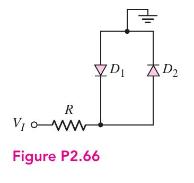
The parameters of \(D_{1}\) and \(D_{2}\) in the circuit shown in Figure P2.66 are \(V_{\gamma}=1.7 \mathrm{~V}\) and \(r_{f}=20 \Omega\). The current in each diode is to be limited to \(I_{D}=15 \mathrm{~mA}\) for \(V_{I}= \pm 5 \mathrm{~V}\). Determine the required value of \(R\). R Figure P2.66
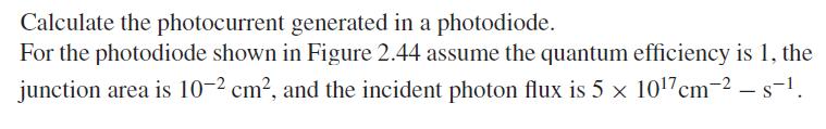
If the resistor in Example 2.12 is \(R=2 \mathrm{k} \Omega\) and the diode is to be reverse biased by at least \(1 \mathrm{~V}\), determine the minimum power supply voltage required.Data From Example 2.12:- Calculate the photocurrent generated in a photodiode. For the photodiode shown in Figure
Consider the photodiode circuit shown in Figure 2.44. Assume the quantum efficiency is 1 . A photocurrent of \(0.6 \mathrm{~mA}\) is required for an incident photon flux of \(\Phi=10^{17} \mathrm{~cm}^{-2}-\mathrm{s}^{-1}\). Determine the required cross-sectional area of the diode. VPS + 1ph hv R
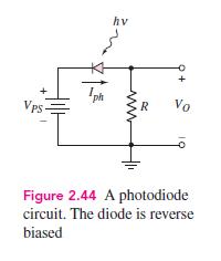
Consider the voltage doubler circuit in Figure 2.14. Assume a \(60 \mathrm{~Hz}\), \(120 \mathrm{~V}\) (rms) signal is applied at the input of the transformer with a \(20: 1\) turns ratio. Let \(R=10 \mathrm{k} \Omega\) and \(C_{1}=C_{2}=200 \mu \mathrm{F}\). Using a computer simulation, plot the
Consider the parameters and results of Example 2.2. Use a computer simulation to plot the output voltage of each rectifier over four cycles of input voltage. Also determine the PIV of each diode. How do the computer results compare with the results of the example?Data From Example 2.2:- Compare
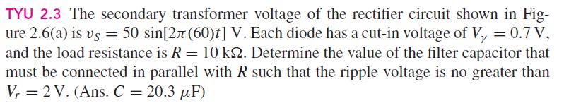
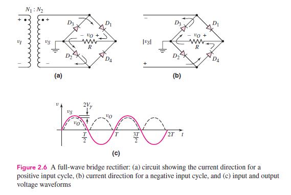
(a) Using a computer simulation, verify the results of Exercise TYU 2.3.(b) Determine the ripple voltage if a filter capacitance of \(C=50 \mu \mathrm{F}\) is connected in parallel with the load resistance.Data From Exercise TYU 2.3:-Figure 2.6:- TYU 2.3 The secondary transformer voltage of the
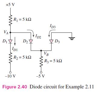
(a) Using a computer simulation, determine each diode current and voltage in the circuit shown in Figure 2.40.(b) Repeat part (a) using the circuit parameters given in Exercise 2.11.Figure 2.40:-Data From Exercise 2.11:-Data From Example 2.11:- +5 V R = 5k VA D ZD27 ID2 Ip3 D3 IDI VB R = 5 k R = 5
Consider the full-wave bridge rectifier circuit. The input signal is \(120 \mathrm{~V}\) (rms) at \(60 \mathrm{~Hz}\). The load resistance is \(R_{L}=250 \Omega\). The peak output voltage is to be \(9 \mathrm{~V}\) and the ripple voltage is to be no more than 5 percent. Determine the required turns
Design a simple dc voltage source using a \(120 \mathrm{~V}(\mathrm{rms}), 60 \mathrm{~Hz}\) input signal to a nominal \(10 \mathrm{~V}\) output signal. A Zener diode with parameters \(V_{Z O}=10 \mathrm{~V}\) and \(r_{z}=3 \Omega\) is available. The rated power of the Zener diode is \(5
A clipper is to be designed such that \(v_{O}=2.5 \mathrm{~V}\) for \(v_{I} \geq 2.5\mathrm{~V}\) and \(v_{O}=-1.25 \mathrm{~V}\) for \(v_{I} \leq-1.25 \mathrm{~V}\).
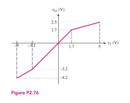
Design a circuit to provide the voltage transfer characteristics shown in Figure P2.76. Use diodes and Zener diodes with appropriate breakdown voltages in the design. The maximum current in the circuit is to be limited to \(1 \mathrm{~mA}\). -312 Figure P2.76 vo (V) 2.5 1.7 -3.2 -4.2 -v (V) 1.7 5
Describe the basic structure and operation of a MOSFET. Define enhancement mode and depletion mode.
Sketch the general current-voltage characteristics for both enhancement-mode and depletion-mode MOSFETs. Define the saturation and nonsaturation bias regions.
Describe what is meant by threshold voltage, width-to-length ratio, and drain-tosource saturation voltage.
Describe the channel length modulation effect and define the parameter \(\lambda\). Describe the body effect and define the parameter \(\gamma\).
Describe a simple common-source MOSFET circuit with an n-channel enhancement-mode device and discuss the relation between the drain-to-source voltage and gate-to-source voltage.
How do you prove that a MOSFET is biased in the saturation region?
In the dc analysis of some MOSFET circuits, quadratic equations in gate-tosource voltage are developed. How do you determine which of the two possible solutions is the correct one?
How can the \(Q\)-point be stabilized against variations in transistor parameters?
Describe the current-voltage relation of an n-channel enhancement-mode MOSFET with the gate connected to the drain.
Describe the current-voltage relation of an n-channel depletion-mode MOSFET with the gate connected to the source.
Describe a MOSFET NOR logic circuit.
Describe how a MOSFET can be used to amplify a time-varying voltage.
Describe the basic operation of a junction FET.
What is the difference between a MESFET and a pn junction FET?
The current in an NMOS transistor is \(0.5 \mathrm{~mA}\) when \(V_{G S}-V_{T N}=0.6 \mathrm{~V}\) and \(1.0 \mathrm{~mA}\) when \(V_{G S}-V_{T N}=1.0 \mathrm{~V}\). The device is operating in the nonsaturation region. Determine \(V_{D S}\) and \(K_{n}\).
For an n-channel depletion-mode MOSFET, the parameters are \(V_{T N}=\) \(-2.5 \mathrm{~V}\) and \(K_{n}=1.1 \mathrm{~mA} / \mathrm{V}^{2}\).(a) Determine \(I_{D}\) for \(V_{G S}=0\); and: (i) \(V_{D S}=\) \(0.5 \mathrm{~V}\), (ii) \(V_{D S}=2.5 \mathrm{~V}\), and (iii) \(V_{D S}=5
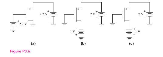
The threshold voltage of each transistor in Figure P3.6 is \(V_{T P}=-0.4 \mathrm{~V}\). Determine the region of operation of the transistor in each circuit. 2.2 V Figure P3.6 (a) 2.2 V 2 V (b) (c) 2 V
Consider an \(\mathrm{n}\)-channel depletion-mode MOSFET with parameters \(V_{T N}=-1.2 \mathrm{~V}\) and \(k_{n}^{\prime}=120 \mu \mathrm{A} / \mathrm{V}^{2}\). The drain current is \(I_{D}=0.5 \mathrm{~mA}\) at \(V_{G S}=0\) and \(V_{D S}=2 \mathrm{~V}\). Determine the \(W / L\) ratio.
Determine the value of the process conduction parameter \(k_{n}^{\prime}\) for an NMOS transistor with \(\mu_{n}=600 \mathrm{~cm}^{2} / \mathrm{V}-\mathrm{s}\) and for an oxide thickness \(t_{\mathrm{ox}}\) of (a) \(500 Å\), (b) \(250 Å\), (c) \(100 Å\), (d) \(50 Å\), and (e) \(25 Å\).
An n-channel enhancement-mode MOSFET has parameters \(V_{T N}=0.4 \mathrm{~V}\), \(W=20 \mu \mathrm{m}, L=0.8 \mu \mathrm{m}, t_{\mathrm{ox}}=200 Å\), and \(\mu_{n}=650 \mathrm{~cm}^{2} / \mathrm{V}-\mathrm{s}\).(a) Calculate the conduction parameter \(K_{n}\).(b) Determine the drain current when
An NMOS device has parameters \(V_{T N}=0.8 \mathrm{~V}, L=0.8 \mu \mathrm{m}\), and \(k_{n}^{\prime}=120 \mu \mathrm{A} / \mathrm{V}^{2}\). When the transistor is biased in the saturation region with \(V_{G S}=1.4 \mathrm{~V}\), the drain current is \(I_{D}=0.6 \mathrm{~mA}\). (a) What is the
A particular NMOS device has parameters \(V_{T N}=0.6 \mathrm{~V}, L=0.8 \mu \mathrm{m}\), \(t_{\mathrm{ox}}=200 Å\), and \(\mu_{n}=600 \mathrm{~cm}^{2} / \mathrm{V}-\mathrm{s}\). A drain current of \(I_{D}=1.2 \mathrm{~mA}\) is required when the device is biased in the saturation region at \(V_{G
MOS transistors with very short channels do not exhibit the square law voltage relation in saturation. The drain current is instead given by\(I_{D}=W C_{\mathrm{ox}}\left(V_{G S}-V_{T N}\right) v_{\mathrm{sat}}\)where \(v_{\text {sat }}\) is a saturation velocity. Assuming \(v_{\text {sat }}=2
For a p-channel enhancement-mode MOSFET, \(k_{p}^{\prime}=50 \mu \mathrm{A} / \mathrm{V}^{2}\). The device has drain currents of \(I_{D}=0.225 \mathrm{~mA}\) at \(V_{S G}=V_{S D}=2 \mathrm{~V}\) and \(I_{D}=0.65 \mathrm{~mA}\) at \(V_{S G}=V_{S D}=3 \mathrm{~V}\). Determine the \(W / L\) ratio and
For a p-channel enhancement-mode MOSFET, the parameters are \(K_{P}=\) \(2 \mathrm{~mA} / \mathrm{V}^{2}\) and \(V_{T P}=-0.5 \mathrm{~V}\). The gate is at ground potential, and the source and substrate terminals are at \(+5 \mathrm{~V}\). Determine \(I_{D}\) when the drain terminal voltage is: (a)
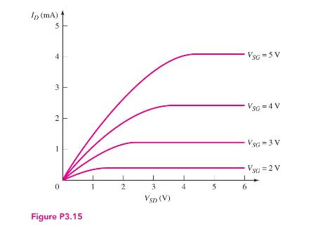
The transistor characteristics \(i_{D}\) versus \(v_{S D}\) for a PMOS device are shown in Figure P3.15. (a) Is this an enhancement-mode or depletion-mode device?(b) Determine the values for \(K_{p}\) and \(V_{T P}\). (c) Determine \(i_{D}\) (sat) for \(v_{S G}=3.5 \mathrm{~V}\) and \(v_{S G}=4.5
A p-channel depletion-mode MOSFET has parameters \(V_{T P}=+2 \mathrm{~V}\), \(k_{p}^{\prime}=40 \mu \mathrm{A} / \mathrm{V}^{2}\), and \(W / L=6\). Determine \(V_{S D}\) (sat) for: (a) \(V_{S G}=-1 \mathrm{~V}\), (b) \(V_{S G}=0\), and (c) \(V_{S G}=+1 \mathrm{~V}\). If the transistor is biased in
Calculate the drain current in a PMOS transistor with parameters \(V_{T P}=-0.5 \mathrm{~V}, k_{p}^{\prime}=50 \mu \mathrm{A} / \mathrm{V}^{2}, W=12 \mu \mathrm{m}, L=0.8 \mu \mathrm{m}\), and with applied voltages of \(V_{S G}=2 \mathrm{~V}\) and (a) \(V_{S D}=0.2 \mathrm{~V}\), (b) \(V_{S D}=0.8
Determine the value of the process conduction parameter \(k_{p}^{\prime}\) for a PMOS transistor with \(\mu_{p}=250 \mathrm{~cm}^{2} / \mathrm{V}-\mathrm{s}\) and for an oxide thickness \(t_{\mathrm{ox}}\) of(a) \(500 Å\),(b) \(250 Å\),(c) \(100 Å\),(d) \(50 Å\), and(e) \(25 Å\).
Enhancement-mode NMOS and PMOS devices both have parameters \(L=4 \mu \mathrm{m}\) and \(t_{\mathrm{ox}}=500 Å\). For the NMOS transistor, \(V_{T N}=+0.6 \mathrm{~V}\), \(\mu_{n}=675 \mathrm{~cm}^{2} / \mathrm{V}-\mathrm{s}\), and the channel width is \(W_{n}\); for the PMOS transistor, \(V_{T
For an NMOS enhancement-mode transistor, the parameters are: \(V_{T N}=\) \(1.2 \mathrm{~V}, K_{n}=0.20 \mathrm{~mA} / \mathrm{V}^{2}\), and \(\lambda=0.01 \mathrm{~V}^{-1}\). Calculate the output resistance \(r_{o}\) for \(V_{G S}=2.0 \mathrm{~V}\) and for \(V_{G S}=4.0 \mathrm{~V}\). What is the
The parameters of an n-channel enhancement-mode MOSFET are \(V_{T N}=0.5 \mathrm{~V}, k_{n}^{\prime}=120 \mu \mathrm{A} / \mathrm{V}^{2}\), and \(W / L=4\). What is the maximum value of \(\lambda\) and the minimum value of \(V_{A}\) such that for \(V_{G S}=2 \mathrm{~V}, r_{o} \geq 200 \mathrm{k}
An enhancement-mode NMOS transistor has parameters \(V_{T N O}=0.8 \mathrm{~V}\), \(\gamma=0.8 \mathrm{~V}^{1 / 2}\), and \(\phi_{f}=0.35 \mathrm{~V}\). At what value of \(V_{S B}\) will the threshold voltage change by \(2 \mathrm{~V}\) due to the body effect?
An NMOS transistor has parameters \(V_{T O}=0.75 \mathrm{~V}, k_{n}^{\prime}=80 \mu \mathrm{A} / \mathrm{V}^{2}\), \(W / L=15, \phi_{f}=0.37 \mathrm{~V}\), and \(\gamma=0.6 \mathrm{~V}^{1 / 2}\).(a) The transistor is biased at \(V_{G S}=2.5 \mathrm{~V}, V_{S B}=3 \mathrm{~V}\), and \(V_{D S}=3
(a) A silicon dioxide gate insulator of an MOS transistor has a thickness of \(t_{\mathrm{ox}}=120 Å\). (i) Calculate the ideal oxide breakdown voltage. (ii) If a safety factor of three is required, determine the maximum safe gate voltage that may be applied.(b) Repeat part (a) for an oxide
In a power MOS transistor, the maximum applied gate voltage is \(24 \mathrm{~V}\). If a safety factor of three is specified, determine the minimum thickness necessary for the silicon dioxide gate insulator.
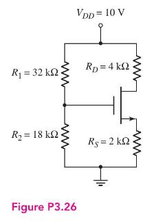
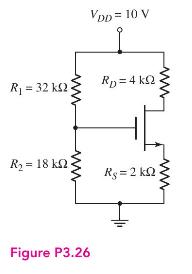
In the circuit in Figure P3.26, the transistor parameters are \(V_{T N}=0.8 \mathrm{~V}\) and \(K_{n}=0.5 \mathrm{~mA} / \mathrm{V}^{2}\). Calculate \(V_{G S}, I_{D}\), and \(V_{D S}\). VDD = 10 V R = 32 k RD=4 k2 R2 = 18 = 2 Figure P3.26
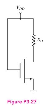
The transistor in the circuit in Figure P3.27 has parameters \(V_{T N}=0.8 \mathrm{~V}\) and \(K_{n}=0.25 \mathrm{~mA} / \mathrm{V}^{2}\). Sketch the load line and plot the \(Q\)-point for (a) \(V_{D D}=4 \mathrm{~V}, R_{D}=1 \mathrm{k} \Omega\) and (b) \(V_{D D}=5 \mathrm{~V}, R_{D}=3 \mathrm{k}
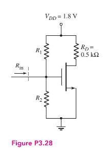
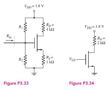
The transistor in Figure P3.28 has parameters VTN = 0.4V, k = 120 A/V, and W/L = 80. Design the circuit such that IQ = 0.8mA and Rin = 200 ks2. Rin VDD = 1.8 V RD= R 0.5 R- www Figure P3.28
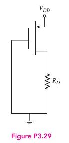
The transistor in the circuit in Figure P3.29 has parameters VTP = -0.8 V and Kp = 0.20mA/V. Sketch the load line and plot the Q-point for (a) VDD 3.5V, RD = 1.2k2 and (b) VDD = 5 V, RD = 4k. What is the operating bias region for each condition? VDD Figure P3.29 Rp.
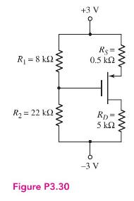
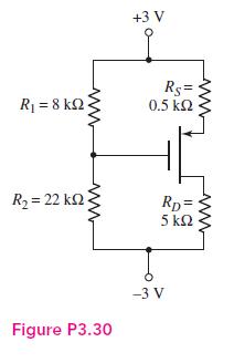
Consider the circuit in Figure P3.30. The transistor parameters are VTP = -0.8 V and Kp = 0.5mA/V. Determine ID, VSG, and VSD. R = 8 k2 R 22 ks22 ww ww Figure P3.30 -3 V +3 V Rs = 0.5 RD= 5
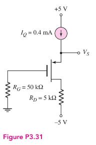
For the circuit in Figure P3.31, the transistor parameters are Vp = -0.8 V and Kp = 200 A/V. Determine Vs and VSD. +5 V IQ = 0.4 mA (+ Vs RG = 50kQ RD=5k2 Figure P3.31 -5 V
Design a MOSFET circuit in the configuration shown in Figure P3.26. The transistor parameters are VTN = 0.4V and k = 120 A/V, and = 0. The circuit parameters are VDD =3.3V and Rp = 5 k2. Design the circuit so that VpsQ 1.6V and the voltage across Rs is approximately 0.8V. Set VGS = 0.8V. The
Consider the circuit shown in Figure P3.33. The transistor parameters are \(V_{T N}=0.4 \mathrm{~V}\) and \(k_{n}^{\prime}=120 \mu \mathrm{A} / \mathrm{V}^{2}\). The voltage drop across \(R_{S}\) is to be \(0.20 \mathrm{~V}\). Design the transistor \(W / L\) ratio such that \(V_{D S}=V_{D S}\)
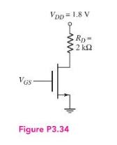
The transistor parameters for the transistor in Figure P3.34 are \(V_{T N}=0.4 \mathrm{~V}, k_{n}^{\prime}=120 \mu \mathrm{A} / \mathrm{V}^{2}\), and \(W / L=50\). (a) Determine \(V_{G S}\) such that \(I_{D}=0.35 \mathrm{~mA}\). (b) Determine \(V_{D S}\) and \(V_{D S}\) (sat). VDD = 1.8 V Rp= 2
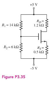
For the transistor in the circuit in Figure P3.35, the parameters are \(V_{T N}=0.4 \mathrm{~V}, k_{n}^{\prime}=120 \mu \mathrm{A} / \mathrm{V}^{2}\), and \(W / L=25\). Determine \(V_{G S}, I_{D}\), and \(V_{D S}\). Sketch the load line and plot the \(Q\)-point. +5 V R = 14 R = 1.2 R 6 ks2 Rs=
Design a MOSFET circuit with the configuration shown in Figure P3.30. The transistor parameters are \(V_{T P}=-0.6 \mathrm{~V}, k_{p}^{\prime}=50 \mu \mathrm{A} / \mathrm{V}^{2}\), and \(\lambda=0\). The circuit bias is \(\pm 3 \mathrm{~V}\), the drain current is to be \(0.2 \mathrm{~mA}\), the
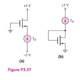
The parameters of the transistors in Figures P3.37 (a) and (b) are \(K_{n}=\) \(0.5 \mathrm{~mA} / \mathrm{V}^{2}, V_{T N}=1.2 \mathrm{~V}\), and \(\lambda=0\). Determine \(v_{G S}\) and \(v_{D S}\) for each transistor when (i) \(I_{Q}=50 \mu \mathrm{A}\) and (ii) \(I_{Q}=1 \mathrm{~mA}\). I +5 V
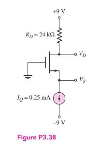
For the circuit in Figure P3.38, the transistor parameters are \(V_{T N}=0.6 \mathrm{~V}\) and \(K_{n}=200 \mu \mathrm{A} / \mathrm{V}^{2}\). Determine \(V_{S}\) and \(V_{D}\). +9 V Rp=24 kQ VD 10-0.25 mA (+ Figure P3.38 -9 V Vs
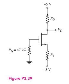
(a) Design the circuit in Figure P3.39 such that \(I_{D Q}=0.50 \mathrm{~mA}\) and \(V_{D}=\) \(1 \mathrm{~V}\). The transistor parameters are \(K_{n}=0.25 \mathrm{~mA} / \mathrm{V}^{2}\) and \(V_{T N}=1.4 \mathrm{~V}\). Sketch the load line and plot the \(Q\)-point.(b) Choose standard resistor
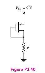
The PMOS transistor in Figure P3.40 has parameters \(V_{T P}=-0.7 \mathrm{~V}\), \(k_{p}^{\prime}=50 \mu \mathrm{A} / \mathrm{V}^{2}, L=0.8 \mu \mathrm{m}\), and \(\lambda=0\). Determine the values of \(W\) and \(R\) such that \(I_{D}=0.1 \mathrm{~mA}\) and \(V_{S D}=2.5 \mathrm{~V}\). VDD=9 V ww R
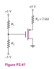
Design the circuit in Figure P3.41 so that \(V_{S D}=2.5 \mathrm{~V}\). The current in the bias resistors should be no more than 10 percent of the drain current. The transistor parameters are \(V_{T P}=+1.5 \mathrm{~V}\) and \(K_{p}=0.5 \mathrm{~mA} / \mathrm{V}^{2}\). +5 V +5 V www R Rs = 2 ks2 R
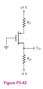
(a) Design the circuit in Figure P3.42 such that \(I_{D Q}=0.25 \mathrm{~mA}\) and \(V_{D}=-2 \mathrm{~V}\). The nominal transistor parameters are \(V_{T P}=-1.2 \mathrm{~V}, k_{p}^{\prime}=\) \(35 \mu \mathrm{A} / \mathrm{V}^{2}\), and \(W / L=15\). Sketch the load line and plot the \(Q\)-point.
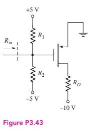
The parameters of the transistor in the circuit in Figure P3.43 are \(V_{T P}=\) \(-1.75 \mathrm{~V}\) and \(K_{p}=3 \mathrm{~mA} / \mathrm{V}^{2}\). Design the circuit such that \(I_{D}=5 \mathrm{~mA}\), \(V_{S D}=6 \mathrm{~V}\), and \(R_{\text {in }}=80 \mathrm{k} \Omega\). +5 V Ria R www -5 V
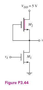
For each transistor in the circuit in Figure P3.44, \(k_{n}^{\prime}=120 \mu \mathrm{A} / \mathrm{V}^{2}\). Also for \(M_{1}, W / L=4\) and \(V_{T N}=0.4 \mathrm{~V}\), and for \(M_{2}, W / L=1\) and \(V_{T N}=-0.6 \mathrm{~V}\). (a) Determine the input voltage such that both \(M_{1}\) and
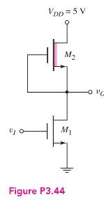
Consider the circuit in Figure P3.44. The transistor parameters for \(M_{1}\) are \(V_{T N}=0.4 \mathrm{~V}\) and \(k_{n}^{\prime}=120 \mu \mathrm{A} / \mathrm{V}^{2}\), and for \(M_{2}\) are \(V_{T N}=-0.6 \mathrm{~V}\), \(k_{n}^{\prime}=120 \mu \mathrm{A} / \mathrm{V}^{2}\), and \(W / L=1\).
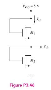
The transistors in the circuit in Figure P3.46 both have parameters \(V_{T N}=0.4 \mathrm{~V}\) and \(k_{n}^{\prime}=120 \mu \mathrm{A} / \mathrm{V}^{2}\).(a) If the width-to-length ratios of \(M_{1}\) and \(M_{2}\) are \((W / L)_{1}=(W / L)_{2}=30\), determine \(V_{G S 1}, V_{G S 2}, V_{O}\), and
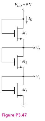
Consider the circuit in Figure P3.47. (a) The nominal transistor parameters are \(V_{T N}=0.6 \mathrm{~V}\) and \(k_{n}^{\prime}=120 \mu \mathrm{A} / \mathrm{V}^{2}\). Design the width-to-length ratio required in each transistor such that \(I_{D Q}=0.8 \mathrm{~mA}, V_{1}=2.5 \mathrm{~V}\), and
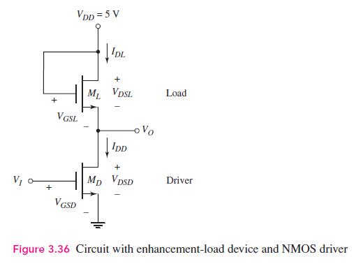
The transistors in the circuit in Figure 3.36 in the text have parameters \(V_{T N}=0.6 \mathrm{~V}, k_{n}^{\prime}=120 \mu \mathrm{A} / \mathrm{V}^{2}\), and \(\lambda=0\). The width-to-length ratio of \(M_{L}\) is \((W / L)_{L}=2\). Design the width-to-length ratio of the driver transistor such
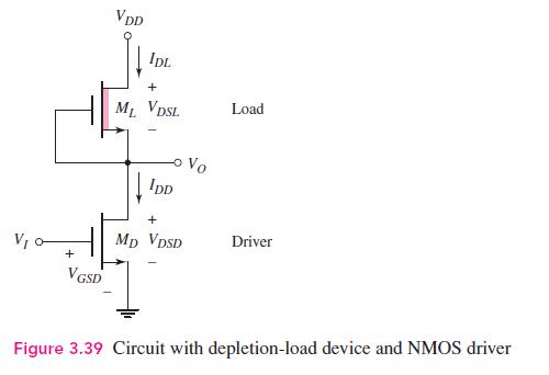
For the circuit in Figure 3.39 in the text, the transistor parameters are: \(V_{T N D}=0.6 \mathrm{~V}, \quad V_{T N L}=-1.2 \mathrm{~V}, \quad \lambda=0, \quad\) and \(\quad k_{n}^{\prime}=120 \mu \mathrm{A} / \mathrm{V}^{2}\). Let \(V_{D D}=5 \mathrm{~V}\). The width-to-length ratio of \(M_{L}\)
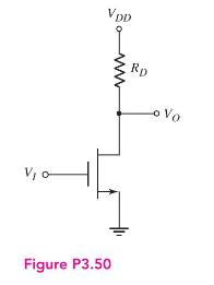
Consider the circuit in Figure P3.50. The circuit parameters are \(V_{D D}=3 \mathrm{~V}\) and \(R_{D}=30 \mathrm{k} \Omega\). The transistor parameters are \(V_{T N}=0.4 \mathrm{~V}\) and \(k_{n}^{\prime}=120 \mu \mathrm{A} / \mathrm{V}^{2}\).(a) Determine the transistor width-to-length ratio such
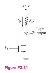
The transistor in the circuit in Figure P3.51 is used to turn the LED on and off. The transistor parameters are \(V_{T N}=0.6 \mathrm{~V}, k_{n}^{\prime}=80 \mu \mathrm{A} / \mathrm{V}^{2}\), and \(\lambda=0\). The diode cut-in voltage is \(V_{\gamma}=1.6 \mathrm{~V}\). Design \(R_{D}\) and the
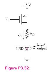
The circuit in Figure P3.52 is another configuration used to switch an LED on and off. The transistor parameters are \(V_{T P}=-0.6 \mathrm{~V}, k_{p}^{\prime}=40 \mu \mathrm{A} / \mathrm{V}^{2}\), and \(\lambda=0\). The diode cut-in voltage is \(V_{\gamma}=1.6 \mathrm{~V}\). Design \(R_{D}\) and
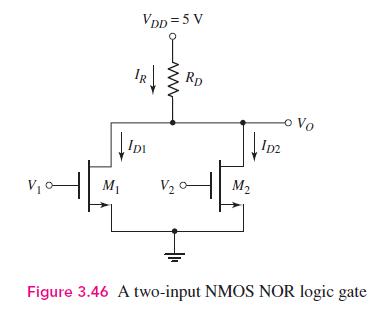
For the two-input NMOS NOR logic gate in Figure 3.46 in the text, the transistor parameters are \(V_{T N 1}=V_{T N 2}=0.6 \mathrm{~V}, \lambda_{1}=\lambda_{2}=0\), and \(k_{n 1}^{\prime}=k_{n 2}^{\prime}=\) \(120 \mu \mathrm{A} / \mathrm{V}^{2}\). The drain resistor is \(R_{D}=50 \mathrm{k}
All transistors in the current-source circuit shown in Figure 3.49 (a) in the text have parameters \(V_{T N}=0.4 \mathrm{~V}, k_{n}^{\prime}=120 \mu \mathrm{A} / \mathrm{V}^{2}\), and \(\lambda=0\). Transistors \(M_{1}\) and \(M_{2}\) are matched. The bias sources are \(V^{+}=2.5 \mathrm{~V}\) and
All transistors in the current-source circuit shown in Figure 3.49 (b) in the text have parameters \(V_{T P}=-0.4 \mathrm{~V}, k_{p}^{\prime}=50 \mu \mathrm{A} / \mathrm{V}^{2}\), and \(\lambda=0\). The bias sources are \(V^{+}=5 \mathrm{~V}\) and \(V^{-}=-5 \mathrm{~V}\). The currents are to be
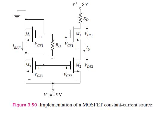
Consider the circuit shown in Figure 3.50 in the text. The threshold voltage and process conduction parameter for each transistor is \(V_{T N}=0.6 \mathrm{~V}\) and \(k_{n}^{\prime}=120 \mu \mathrm{A} / \mathrm{V}^{2}\). Let \(\lambda=0\) for all transistors. Assume that \(M_{1}\) and \(M_{2}\) are
The gate and source of an n-channel depletion-mode JFET are connected together. What value of \(V_{D S}\) will ensure that this two-terminal device is biased in the saturation region. What is the drain current for this bias condition?
For an n-channel JFET, the parameters are \(I_{D S S}=6 \mathrm{~mA}\) and \(V_{P}=-3 \mathrm{~V}\). Calculate \(V_{D S}\) (sat). If \(V_{D S}>V_{D S}\) (sat), determine \(I_{D}\) for: (a) \(V_{G S}=0\), (b) \(V_{G S}=-1 \mathrm{~V}\), (c) \(V_{G S}=-2 \mathrm{~V}\), and (d) \(V_{G S}=-3
A p-channel JFET biased in the saturation region with \(V_{S D}=5 \mathrm{~V}\) has a drain current of \(I_{D}=2.8 \mathrm{~mA}\) at \(V_{G S}=1 \mathrm{~V}\) and \(I_{D}=0.30 \mathrm{~mA}\) at \(V_{G S}=3 \mathrm{~V}\). Determine \(I_{D S S}\) and \(V_{P}\).
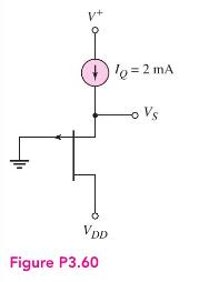
Consider the p-channel JFET in Figure P3.60. Determine the range of \(V_{D D}\) that will bias the transistor in the saturation region. If \(I_{D S S}=6 \mathrm{~mA}\) and \(V_{P}=2.5 \mathrm{~V}\), find \(V_{S}\). +1=2mA - Vs VDD Figure P3.60
Consider a GaAs MESFET. When the device is biased in the saturation region, we find that \(I_{D}=18.5 \mu \mathrm{A}\) at \(V_{G S}=0.35 \mathrm{~V}\) and \(I_{D}=86.2 \mu \mathrm{A}\) at \(V_{G S}=0.50 \mathrm{~V}\). Determine the conduction parameter \(k\) and the threshold voltage \(V_{T N}\).
The threshold voltage of a GaAs MESFET is \(V_{T N}=0.24 \mathrm{~V}\). The maximum allowable gate-to-source voltage is \(V_{G S}=0.75 \mathrm{~V}\). When the transistor is biased in the saturation region, the maximum drain current is \(I_{D}=250 \mu \mathrm{A}\). What is the value of the
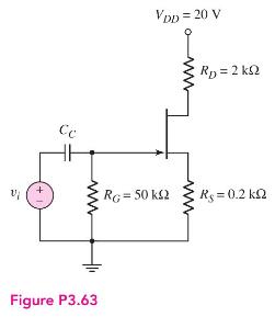
For the transistor in the circuit in Figure P3.63, the parameters are: \(I_{D S S}=\) \(10 \mathrm{~mA}\) and \(V_{P}=-5 \mathrm{~V}\). Determine \(I_{D Q}, V_{G S Q}\), and \(V_{D S Q}\). Cc VDD = 20 V RD = 2 k V RG = 50 k2 Rs = 0.2 k Figure P3.63
Showing 1600 - 1700
of 4723
First
10
11
12
13
14
15
16
17
18
19
20
21
22
23
24
Last
Step by Step Answers