New Semester
Started
Get
50% OFF
Study Help!
--h --m --s
Claim Now
Question Answers
Textbooks
Find textbooks, questions and answers
Oops, something went wrong!
Change your search query and then try again
S
Books
FREE
Study Help
Expert Questions
Accounting
General Management
Mathematics
Finance
Organizational Behaviour
Law
Physics
Operating System
Management Leadership
Sociology
Programming
Marketing
Database
Computer Network
Economics
Textbooks Solutions
Accounting
Managerial Accounting
Management Leadership
Cost Accounting
Statistics
Business Law
Corporate Finance
Finance
Economics
Auditing
Tutors
Online Tutors
Find a Tutor
Hire a Tutor
Become a Tutor
AI Tutor
AI Study Planner
NEW
Sell Books
Search
Search
Sign In
Register
study help
computer science
systems analysis and design 12th
Microelectronics Circuit Analysis And Design 4th Edition Donald A. Neamen - Solutions
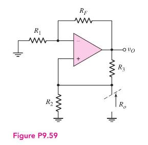
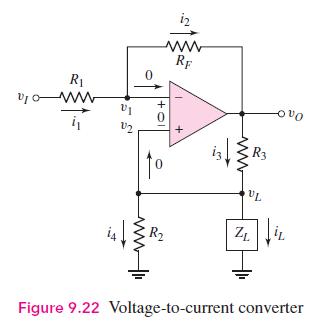
Figure P9.59 is used to calculate the resistance seen by the load in the voltage-to-current converter given in Figure 9.22. (a) Show that the output resistance is given by\[R_{o}=\frac{R_{1} R_{2} R_{3}}{R_{1} R_{3}-R_{2} R_{F}}\](b) Using the parameters given in Example 9.5, determine \(R_{o}\).
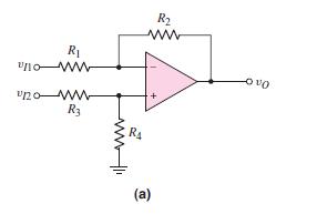
Consider the op-amp difference amplifier in Figure 9.24(a). Let \(R_{1}=R_{3}\) and \(R_{2}=R_{4}\). A load resistor \(R_{L}=10 \mathrm{k} \Omega\) is connected from the output terminal to ground. (a) Design the circuit such that the difference voltage gain is \(A_{d}=15\) and the minimum
Consider the differential amplifier shown in Figure 9.24(a). Let \(R_{1}=R_{3}\) and \(R_{2}=R_{4}\). Design the amplifier such that the differential voltage gain is (a) 40 , (b) 25 , (c) 5 , and (d) 0.5. In each case the differential input resistance should be as large as possible but under the
Consider the differential amplifier shown in Figure 9.24(a). Assume that each resistor is \(50(1 \pm x) \mathrm{k} \Omega\). (a) Determine the worst case common-mode gain \(A_{C M}=v_{O} / v_{C M}\), where \(v_{C M}=v_{1}=v_{2}\). (b) Evaluate \(A_{C M}\) and CMRR \((\mathrm{dB})\) for
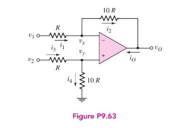
Let \(R=10 \mathrm{k} \Omega\) in the differential amplifier in Figure P9.63. Determine the voltages \(v_{X}, v_{Y}, v_{O}\) and the currents \(i_{1}, i_{2}, i_{3}, i_{4}\) for input voltages of (a) \(v_{1}=1.80 \mathrm{~V}, v_{2}=1.40 \mathrm{~V}\); (b) \(v_{1}=3.20 \mathrm{~V}, v_{2}=3.60
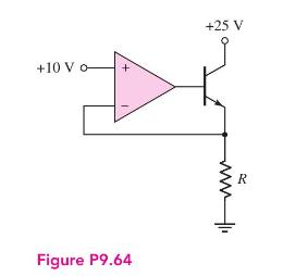
Consider the circuit shown in Figure P9.64.(a) The output current of the op-amp is \(1.2 \mathrm{~mA}\) and the transistor current gain is \(\beta=75\). Determine the resistance \(R\).(b) Repeat part (a) if the current is \(0.2 \mathrm{~mA}\) and the transistor current gain is \(\beta=100\).(c)
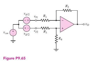
The circuit in Figure P9.65 is a representation of the common-mode and differential-input signals to a difference amplifier. The output voltage can be written as\[v_{O}=A_{d} v_{d}+A_{c m} v_{c m}\]where \(A_{d}\) is the differential-mode gain and \(A_{c m}\) is the common-mode gain.(a) Setting
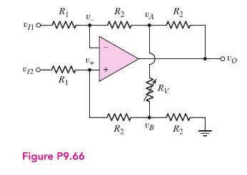
Consider the adjustable gain difference amplifier in Figure P9.66. Variable resistor \(R_{V}\) is used to vary the gain. Show that the output voltage \(v_{O}\), as a function of \(v_{I 1}\) and \(v_{I 2}\), is given by\[v_{O}=\frac{2 R_{2}}{R_{1}}\left(1+\frac{R_{2}}{R_{V}}\right)\left(v_{I 2}-v_{I
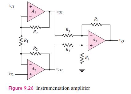
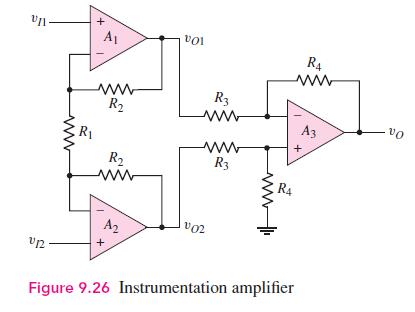
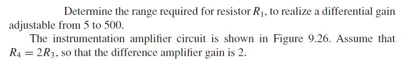
Assume the instrumentation amplifier in Figure 9.26 has ideal op-amps. The circuit parameters are \(R_{1}=10 \mathrm{k} \Omega, R_{2}=40 \mathrm{k} \Omega, R_{3}=40 \mathrm{k} \Omega\), and \(R_{4}=120 \mathrm{k} \Omega\). Determine \(v_{O 1}, v_{O 2}, v_{O}\), and the current in \(R_{1}\) for (a)
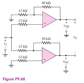
Consider the circuit in Figure P9.68. Assume ideal op-amps are used. The input voltage is \(v_{I}=0.5 \sin \omega t\). Determine the voltages (a) \(v_{O B}\), (b) \(v_{O C}\), and (c) \(v_{O}\). (d) What is the voltage gain \(v_{O} / v_{I}\) ? 12 www 12 www 40 ww + 12 ww 12 www 30 www Figure
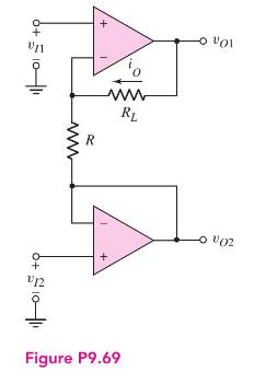
Consider the circuit in Figure P9.69. Assume ideal op-amps are used. (a) Derive the expression for the current \(i_{O}\) as a function of input voltages \(v_{I 1}\) and \(v_{I 2}\). (b) Design the circuit such that \(i_{O}=5 \mathrm{~mA}\) for \(v_{I 1}=0.25 \mathrm{~V}\) and \(v_{I 2}=-0.25
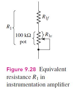
The instrumentation amplifier in Figure 9.26 has the same circuit parameters and input voltages as given in Problem 9.67, except that \(R_{1}\) is replaced by a fixed resistance \(R_{1 f}\) in series with a potentiometer, as shown in Figure 9.28. Determine the values of \(R_{1 f}\) and the
Design the instrumentation amplifier in Figure 9.26 such that the variable differential voltage gain covers the range of 5 to 200 . Set the gain of the difference amplifier to 2.5. The maximum current in \(R_{1}\) is to be limited to \(50 \mu \mathrm{A}\) for an output voltage of \(10
All parameters associated with the instrumentation amplifier in Figure 9.26 are the same as given in Exercise Ex 9.8, except that resistor \(R_{3}\), which is connected to the inverting terminal of \(\mathrm{A} 3\), is \(R_{3}=30 \mathrm{k} \Omega \pm 5 \%\). Determine the maximum common-mode
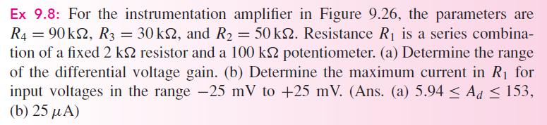
The parameters in the integrator circuit shown in Figure 9.30 are \(R_{1}=20 \mathrm{k} \Omega\) and \(C_{2}=0.02 \mu \mathrm{F}\). The input signal is \(v_{I}=0.25 \cos \omega t(\mathrm{~V})\). (a) Determine the frequency at which the input and output signals have equal amplitudes. At this
Consider the ideal op-amp integrator. Assume the capacitor is initially uncharged. (a) The output voltage is \(v_{O}=-5 \mathrm{~V}\) at \(t=1.2 \mathrm{~s}\) after a \(+0.25 \mathrm{~V}\) pulse is applied to the input. What is the \(R C\) time constant? (b) Use the results of part (a). At \(t=1.2
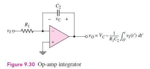
The circuit in Figure P9.75 is a first-order low-pass active filter. (a) Show that the voltage transfer function is given by\[A_{v}=\frac{-R_{2}}{R_{1}} \cdot \frac{1}{1+j \omega R_{2} C_{2}}\](b) What is the voltage gain at dc \((\omega=0)\) ? (c) At what frequency is the magnitude of the voltage
(a) Using the results of Problem 9.75, design the low-pass active filter in Figure P9.75 such that the input resistance is \(20 \mathrm{k} \Omega\), the low-frequency gain is -15 , and the \(-3 \mathrm{~dB}\) frequency is \(5 \mathrm{kHz}\).(b) Repeat part (a) such that the input resistance is \(15
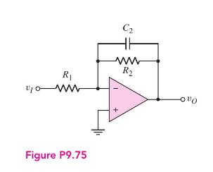
The circuit shown in Figure P9.77 is a first-order high-pass active filter.(a) Show that the voltage transfer function is given by\[A_{v}=\frac{-R_{2}}{R_{1}} \cdot \frac{j \omega R_{1} C_{1}}{1+j \omega R_{1} C_{1}}\](b) What is the voltage gain as the frequency becomes large?(c) At what frequency
(a) Using the results of Problem 9.77, design the high-pass active filter in Figure P9.77 such that the high-frequency voltage gain is -15 and the \(-3 \mathrm{~dB}\) frequency is \(20 \mathrm{kHz}\). The maximum resistance value is to be limited to \(350 \mathrm{k} \Omega\).(b) Repeat part (a)
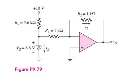
Consider the voltage reference circuit shown in Figure P9.79. Determine \(v_{O}, i_{2}\), and \(i_{\mathrm{Z}}\). Rs = 5.6 kQ +10 V + R = 1 k Vz=6.8 Viz ww Figure P9.79 R = 1 kQ ww
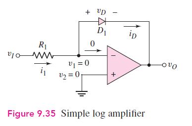
Consider the circuit in Figure 9.35. The diode parameter is \(I_{S}=10^{-14} \mathrm{~A}\) and the resistance is \(R_{1}=10 \mathrm{k} \Omega\). Plot \(v_{O}\) versus \(v_{I}\) over the range \(20 \mathrm{mV} \leq v_{I} \leq 2 \mathrm{~V}\). (Plot \(v_{I}\) on a log scale.) + VD - D iD R i1 V2=01
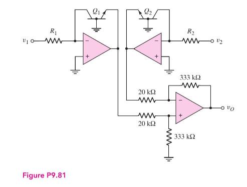
In the circuit in Figure P9.81, assume that \(Q_{1}\) and \(Q_{2}\) are identical transistors. If \(T=300 \mathrm{~K}\), show that the output voltage is\[v_{O}=1.0 \log _{10}\left(\frac{v_{2} R_{1}}{v_{1} R_{2}}\right)\] R ww Figure P9.81 20 ww ww 20 www R 333 333 vo
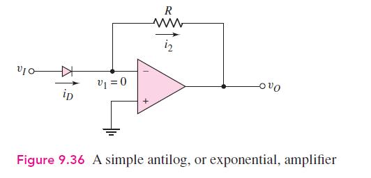
Consider the circuit in Figure 9.36. The diode parameter is \(I_{S}=10^{-14} \mathrm{~A}\) and the resistance is \(R_{1}=10 \mathrm{k} \Omega\). Plot \(v_{O}\) versus \(v_{I}\) for \(0.30 \leq v_{I} \leq\) \(0.60 \mathrm{~V}\). (Plot \(v_{O}\) on a log scale.) R ww i2 K+ v=0 iD Figure 9.36 A simple
Design an op-amp summer to produce the output voltage \(v_{O}=2 v_{I 1}-\) \(10 v_{I 2}+3 v_{I 3}-v_{I 4}\). Assume the largest resistor value is \(500 \mathrm{k} \Omega\), and the input impedance seen by each source is the largest value possible.
Design an op-amp summer to produce an output voltage of \(v_{O}=3 v_{I 1}+\) \(1.5 v_{I 2}+2 v_{I 3}-4 v_{I 4}-6 v_{I 5}\). The largest resistor value is to be \(250 \mathrm{k} \Omega\).
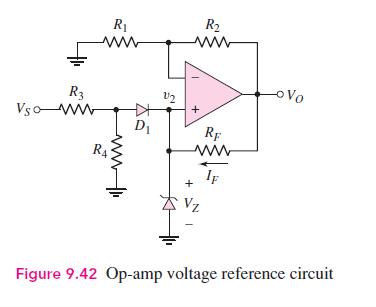
Design a voltage reference source as shown in Figure 9.42 to have an output voltage of \(12.0 \mathrm{~V}\). A Zener diode with a breakdown voltage of \(5.6 \mathrm{~V}\) is available. Assume the voltage regulation will be within specifications if the Zener diode current is within the range of
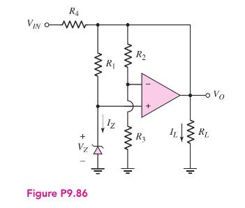
Consider the voltage reference circuit in Figure P9.86. Using a Zener diode with a breakdown voltage of \(5.6 \mathrm{~V}\), design the circuit to produce an output voltage of \(12.0 \mathrm{~V}\). Assume the input voltage is \(15 \mathrm{~V}\) and the Zener diode current is \(I_{Z}=2
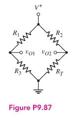
Consider the bridge circuit in Figure P9.87. The resistor \(R_{T}\) is a thermistor with values of \(20 \mathrm{k} \Omega\) at \(T=300 \mathrm{~K}\) and \(21 \mathrm{k} \Omega\) at \(T=350 \mathrm{~K}\). Assume that the thermistor resistance is linear with temperature, and that the bridge is biased
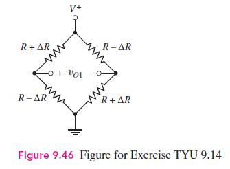
Consider the bridge circuit in Figure 9.46. The resistance \(R\) is \(20 \mathrm{k} \Omega\) and the bias is \(V^{+}=9 \mathrm{~V}\). (a) Determine \(v_{O 1}\) as a function of \(\Delta R\). (b) Design an amplifier system such that the output varies from \(-5 \mathrm{~V}\) to \(+5 \mathrm{~V}\) as
Using a computer simulation, verify the design in Example 9.4.Data From Example 9.4:- Design a summing amplifier to produce a specified output signal. The output signal generated from an ideal amplifier circuit is vo1 = 1.2-0.5 sin oot (V). Design a summing amplifier to be connected to the am-
Using a computer simulation, verify the design in Example 9.8.Data From Example 9.8:- Determine the range required for resistor R, to realize a differential gain adjustable from 5 to 500. The instrumentation amplifier circuit is shown in Figure 9.26. Assume that R4 = 2R3, so that the difference
Using a computer simulation, verify the design in Problem 9.76(b). Plot \(v_{O}\) versus frequency over the range \(2 \leq f \leq 50 \mathrm{kHz}\).Data From Problem 9.76:-(a) Using the results of Problem 9.75, design the low-pass active filter in Figure P9.75 such that the input resistance is \(20
Using a computer simulation, verify the design in Problem 9.78(a). Plot \(v_{O}\) versus frequency over the range \(2 \leq f \leq 100 \mathrm{kHz}\).Data From Problem 9.78:-(a) Using the results of Problem 9.77, design the high-pass active filter in Figure P9.77 such that the high-frequency voltage
(a) Determine the small-signal parameters \(g_{m}, r_{\pi}\), and \(r_{o}\) of a transistor with parameters \(\beta=180\) and \(V_{A}=150 \mathrm{~V}\) for bias currents of (i) \(I_{C Q}=0.5 \mathrm{~mA}\) and (ii) \(I_{C Q}=2 \mathrm{~mA}\).(b) Repeat part (a) for \(\beta=80\) and \(V_{A}=100
(a) The transistor parameters are \(\beta=125\) and \(V_{A}=200 \mathrm{~V}\). A value of \(g_{m}=95 \mathrm{~mA} / \mathrm{V}\) is desired. Determine the required collector current and then find \(r_{\pi}\) and \(r_{o}\). (b) A second transistor has small-signal parameters of \(g_{m}=120
A transistor has a current gain in the range \(90 \leq \beta \leq 180\) and the quiescent collector current is in the range \(0.8 \leq I_{C Q} \leq 1.2\mathrm{~mA}\). What is the possible range in the small-signal parameters \(g_{m}\) and \(r_{\pi}\) ?
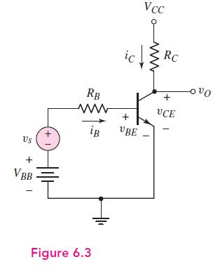
The transistor in Figure 6.3 has parameters \(\beta=120\) and \(V_{A}=\infty\). The circuit parameters are \(V_{C C}=3.3 \mathrm{~V}, R_{C}=15 \mathrm{k} \Omega\), and \(I_{C Q}=0.12 \mathrm{~mA}\). A small signal \(v_{b e}=5 \sin \omega t \mathrm{mV}\) is applied. (a) Determine \(i_{C}\) and
For the circuit in Figure 6.3, the transistor parameters are \(\beta=120\), \(V_{B E}(\mathrm{on})=0.7 \mathrm{~V}\), and \(V_{A}=80 \mathrm{~V}\). The circuit parameters are \(V_{C C}=3.3 \mathrm{~V}\), \(V_{B B}=1.10 \mathrm{~V}, R_{C}=4 \mathrm{k} \Omega\), and \(R_{B}=110 \mathrm{k} \Omega\).
For the circuit in Figure 6.3, \(\beta=120, V_{C C}=5 \mathrm{~V}, V_{A}=100 \mathrm{~V}\), and \(R_{B}=25 \mathrm{k} \Omega\). (a) Determine \(V_{B B}\) and \(R_{C}\) such that \(r_{\pi}=5.4 \mathrm{k} \Omega\) and the \(Q-\) point is in the center of the load line. (b) Find the resulting
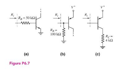
The parameters of each transistor in the circuits shown in Figure P6.7 are \(\beta=120\) and \(I_{C Q}=0.5 \mathrm{~mA}\). Determine the input resistance \(R_{i}\) for each circuit. R V+ R R Rg 50 k21 = ww RB= 100 (a) Figure P6.7 (b) (c) RC= 4
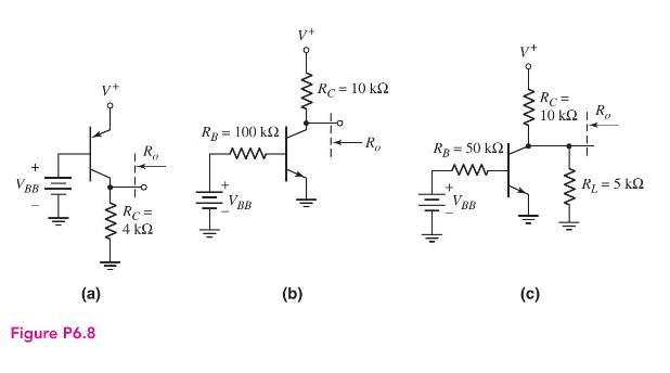
The parameters of each transistor in the circuits shown in Figure P6.8 are \(\beta=130, V_{A}=80 \mathrm{~V}\), and \(I_{C Q}=0.2 \mathrm{~mA}\). Determine the output resistance \(R_{o}\) for each circuit. BB V+ (a) Figure P6.8 Ro Rc= 4 RB = 100 k2 www VBB V+ Rc= 10 ks (b) Ro V+ to ww RB = 50 k2|
The circuit in Figure 6.3 is biased at \(V_{C C}=10 \mathrm{~V}\) and has a collector resistor of \(R_{C}=4 \mathrm{k} \Omega\). The voltage \(V_{B B}\) is adjusted such that \(V_{C}=4 \mathrm{~V}\). The transistor has \(\beta=100\). The signal voltage between the base and emitter is \(v_{b e}=5
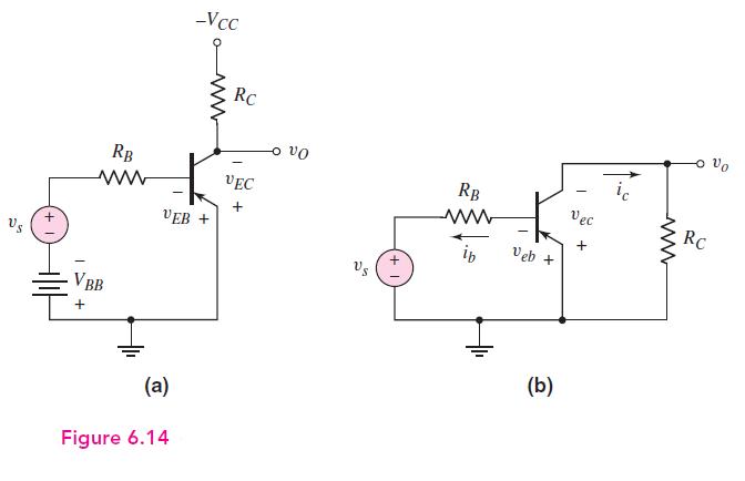
For the circuit in Figure 6.14, \(\beta=100, V_{A}=\infty, V_{C C}=10 \mathrm{~V}\), and \(R_{B}=50 \mathrm{k} \Omega\). (a) Determine \(V_{B B}\) and \(R_{C}\) such that \(I_{C Q}=0.5 \mathrm{~mA}\) and the \(Q\)-point is in the center of the load line. (b) Find the small-signal parameters
The ac equivalent circuit shown in Figure 6.7 has \(R_{C}=2 \mathrm{k} \Omega\). The transistor parameters are \(g_{m}=50 \mathrm{~mA} / \mathrm{V}\) and \(\beta=100\). The time-varying output voltage is given by \(v_{o}=1.2 \sin \omega t(\mathrm{~V})\). Determine \(v_{b e}(t)\) and \(i_{b}(t)\).
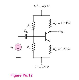
The parameters of the transistor in the circuit in Figure P6.12 are \(\beta=150\) and \(V_{A}=\infty\). (a) Determine \(R_{1}\) and \(R_{2}\) to obtain a bias-stable circuit with the \(Q\)-point in the center of the load line. (b) Determine the small-signal voltage gain \(A_{v}=v_{o} / v_{s}\). Us
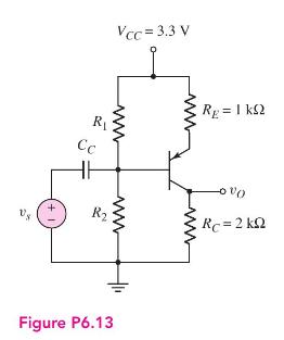
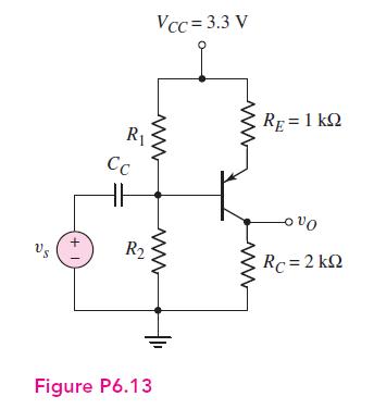
Assume that \(\beta=100, V_{A}=\infty, R_{1}=33 \mathrm{k} \Omega\), and \(R_{2}=50 \mathrm{k} \Omega\) for the circuit in Figure P6.13. (a) Plot the \(Q\)-point on the dc load line. (b) Determine the small-signal voltage gain. (c) Determine the range in voltage gain if \(R_{1}\) and \(R_{2}\) vary
The transistor parameters for the circuit in Figure P6.13 are \(\beta=100\) and \(V_{A}=\infty\). (a) Design the circuit such that it is bias stable and that the \(Q\)-point is in the center of the load line. (b) Determine the small-signal voltage gain of the designed circuit. +1 Vcc = 3.3 V R Cc
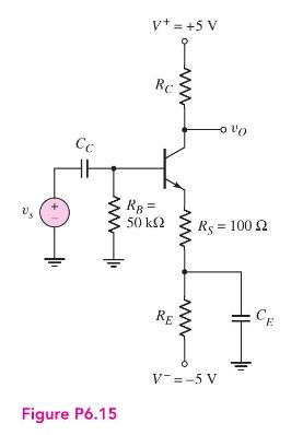
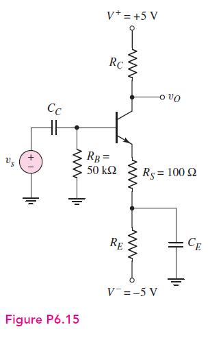
For the circuit in Figure P6.15, the transistor parameters are \(\beta=100\) and \(V_{A}=\infty\). Design the circuit such that \(I_{C Q}=0.25 \mathrm{~mA}\) and \(V_{C E Q}=3 \mathrm{~V}\). Find the small-signal voltage gain \(A_{v}=v_{o} / v_{s}\). Find the input resistance seen by the signal
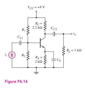
Assume the transistor in the circuit in Figure P6.16 has parameters \(\beta=120\) and \(V_{A}=100 \mathrm{~V}\). (a) Design a bias-stable circuit such that \(V_{C E Q}=5.20 \mathrm{~V}\). (b) Determine the small-signal transresistance function \(R_{m}=v_{o} / i_{s}\). (c) Using the results of part
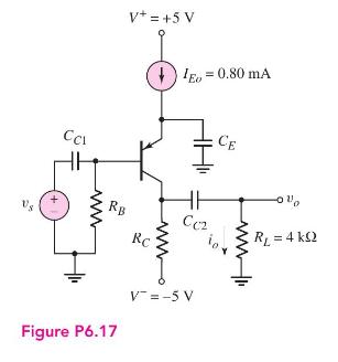
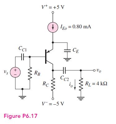
(a) For transistor parameters \(\beta=80\) and \(V_{A}=100 \mathrm{~V}\), (i) design the circuit in Figure P6.17 such that the dc voltages at the base and collector terminals are \(0.20 \mathrm{~V}\) and \(-3 \mathrm{~V}\), respectively, and (ii) determine the small-signal transconductance function
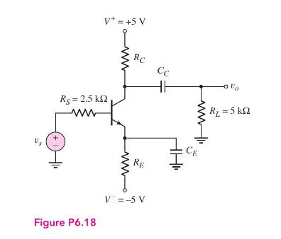
The signal source in Figure P6.18 is \(v_{s}=5 \sin \omega t \mathrm{mV}\). The transistor parameters are \(\beta=120\) and \(V_{A}=\infty\).(a) (i) Design the circuit such that \(I_{C Q}=0.25 \mathrm{~mA}\) and \(V_{C E Q}=3 \mathrm{~V}\). (ii) Find the small-signal voltage gain \(A_{v}=v_{o} /
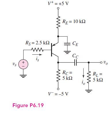
Consider the circuit shown in Figure P6.19 where the signal-source is \(v_{s}=4 \sin \omega t \mathrm{mV}\).(a) For transistor parameters of \(\beta=80\) and \(V_{A}=\infty\), (i) find the small-signal voltage gain \(A_{v}=v_{o} / v_{s}\) and the transconductance function \(G_{f}=i_{o} / v_{s}\),
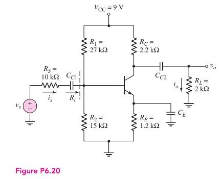
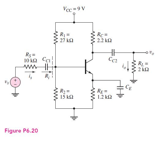
Consider the circuit shown in Figure P6.20. The transistor parameters are \(\beta=100\) and \(V_{A}=100 \mathrm{~V}\). Determine \(R_{i}, A_{v}=v_{o} / v_{s}\), and \(A_{i}=i_{o} / i_{s}\). Vcc = 9 V R = 27 KS2 RC= 2.2 ww R = 2 Rs= 10 k2 CC ww R i www R = 15 CC2 RE= 1.2 CE +1 Figure P6.20
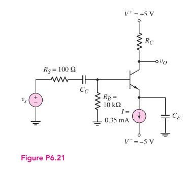
The parameters of the transistor in the circuit in Figure P6.21 are \(\beta=100\) and \(V_{A}=100 \mathrm{~V}\).(a) Find the dc voltages at the base and emitter terminals.(b) Find \(R_{C}\) such that \(V_{C E Q}=3.5 \mathrm{~V}\).(c) Assuming \(C_{C}\) and \(C_{E}\) act as short circuits, determine
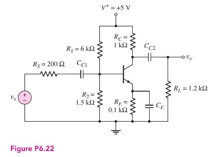
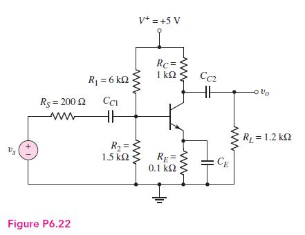
For the circuit in Figure P6.22, the transistor parameters are \(\beta=180\) and \(r_{o}=\infty\). (a) Determine the \(Q\)-point values. (b) Find the small-signal hybrid- \(\pi\) parameters. (c) Find the small-signal voltage gain \(A_{v}=v_{o} / v_{s}\). + Rs = 200 2 ww Figure P6.22 R = 6 CCL HH R
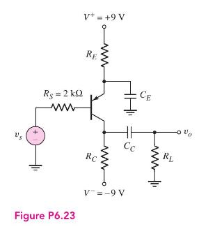
For the circuit in Figure P6.23, the transistor parameters are \(\beta=80\) and \(V_{A}=80 \mathrm{~V}\). (a) Determine \(R_{E}\) such that \(I_{E Q}=0.75 \mathrm{~mA}\). (b) Determine \(R_{C}\) such that \(V_{E C Q}=7 \mathrm{~V}\). (c) For \(R_{L}=10 \mathrm{k} \Omega\), determine the
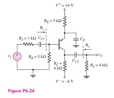
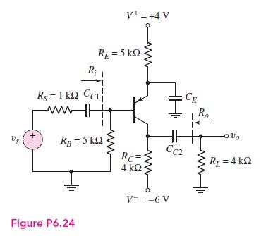
The transistor in the circuit in Figure P6.24 has parameters \(V_{E B}(\mathrm{on})=0.7 \mathrm{~V}\), \(V_{A}=50 \mathrm{~V}\), and a current gain in the range \(80 \leq \beta \leq 120\). Determine (a) the range in the small-signal voltage gain \(A_{v}=v_{o} / v_{s}\), (b) the range in the input
Design a one-transistor common-emitter preamplifier that can amplify a \(10 \mathrm{mV}\) (rms) microphone signal and produce a \(0.5 \mathrm{~V}\) (rms) output signal. The source resistance of the microphone is \(1 \mathrm{k} \Omega\). Use standard resistor values in the design and specify the
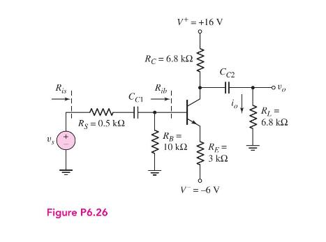
For the transistor in the circuit in Figure P6.26, the parameters are \(\beta=100\) and \(V_{A}=\infty\).(a) Determine the \(Q\)-point.(b) Find the small-signal parameters \(g_{m}, r_{\pi}\), and \(r_{o}\).(c) Find the small-signal voltage gain \(A_{v}=v_{o} / v_{s}\) and the small-signal current
If the collector of a transistor is connected to the base terminal, the transistor continues to operate in the forward-active mode, since the \(\mathrm{B}-\mathrm{C}\) junction is not reverse biased. Determine the small-signal resistance, \(r_{e}=v_{c e} / i_{e}\), of this two-terminal device in
(a) Design an amplifier with the configuration similar to that shown in Figure 6.31. The circuit is to be biased with \(V_{C C}=3.3 \mathrm{~V}\) and the source resistance is \(R_{S}=100 \Omega\). The minimum small-signal voltage gain is to be \(\left|A_{v}\right|=10\). The available npn
An ideal signal voltage source is given by \(v_{s}=5 \sin (5000 t)(\mathrm{mV})\). The peak current that can be supplied by this source is \(0.2 \mu \mathrm{A}\). The desired output voltage across a \(10 \mathrm{k} \Omega\) load resistor is \(v_{o}=100 \sin (5000 t)(\mathrm{mV})\). Design a
Design a one-transistor common-emitter amplifier with a small-signal voltage gain of approximately \(A_{v}=-10\). The circuit is to be biased from a single power supply of \(V_{C C}=5 \mathrm{~V}\) that can supply a maximum current of \(0.8 \mathrm{~mA}\). The input resistance is to be greater than
Design a common-emitter circuit whose output is capacitively coupled to a load resistor \(R_{L}=10 \mathrm{k} \Omega\). The minimum small-signal voltage gain is to be \(\left|A_{v}\right|=50\). The circuit is to be biased at \(\pm 5 \mathrm{~V}\) and each voltage source can supply a maximum of
Consider the circuit shown in Figure P6.13. Assume \(R_{1}=33 \mathrm{k} \Omega\) and \(R_{2}=50 \mathrm{k} \Omega\). The transistor parameters are \(\beta=100\) and \(V_{A}=\infty\). Determine the maximum undistorted swing in the output voltage if the total instantaneous \(\mathrm{E}-\mathrm{C}\)
For the circuit in Figure P6.15, let \(\beta=100, V_{A}=\infty, R_{E}=12.9 \mathrm{k} \Omega\), and \(R_{C}=6 \mathrm{k} \Omega\). Determine the maximum undistorted swing in the output voltage if the total instantaneous \(\mathrm{C}-\mathrm{E}\) voltage is to remain in the range \(1 \leq v_{C E}
Consider the circuit in Figure P6.19. The transistor parameters are \(\beta=80\) and \(V_{A}=\infty\). (a) Determine the maximum undistorted swing in the output voltage if the total instantaneous \(\mathrm{C}-\mathrm{E}\) voltage is to remain in the range \(0.7 \leq v_{C E} \leq 9 \mathrm{~V}\) and
The parameters of the circuit shown in Figure P6.17 are \(R_{B}=20 \mathrm{k} \Omega\) and \(R_{C}=2.5 \mathrm{k} \Omega\). The transistor parameters are \(\beta=80\) and \(V_{A}=\infty\). Determine the maximum undistorted swing in the output current \(i_{o}\) if the total instantaneous collector
Consider the circuit in Figure P6.26 with transistor parameters described in Problem 6.26. Determine the maximum undistorted swing in the output current \(i_{C}\) if the total instantaneous collector current is \(i_{C} \geq 0.1\mathrm{~mA}\) and the total instantaneous C-E voltage is in the range
For the circuit in Figure P6.20, the transistor parameters are \(\beta=100\) and \(V_{A}=100 \mathrm{~V}\). The values of \(R_{C}, R_{E}\), and \(R_{L}\) are as shown in the figure. Design a bias-stable circuit to achieve the maximum undistorted swing in the output voltage if the total
In the circuit in Figure P6.22 with transistor parameters \(\beta=180\) and \(V_{A}=\infty\), redesign the bias resistors \(R_{1}\) and \(R_{2}\) to achieve maximum symmetrical swing in the output voltage and to maintain a bias-stable circuit. The total instantaneous \(\mathrm{C}-\mathrm{E}\)
For the circuit in Figure P6.24, the transistor parameters are \(\beta=100\) and \(V_{A}=\infty\). (a) Determine the maximum undistorted swing in the output voltage if the total instantaneous \(\mathrm{E}-\mathrm{C}\) voltage is to remain in the range \(1 \leq v_{E C} \leq 9 \mathrm{~V}\). (b)
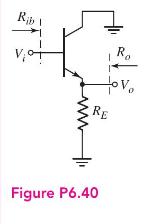
Figure P6.40 shows the ac equivalent circuit of an emitter follower.(a) The transistor parameters are \(\beta=120\) and \(V_{A}=\infty\). For \(R_{E}=500 \Omega\), determine \(I_{C Q}\) such that the small-signal voltage gain is \(A_{v}=0.92\).(b) Using the results of part (a), determine the
Consider the ac equivalent circuit in Figure P6.40. The transistor parameters are \(\beta=80\) and \(V_{A}=\infty\). (a) Design the circuit (find \(I_{C Q}\) and \(R_{E}\) ) such that \(R_{i b}=50 \mathrm{k} \Omega\) and \(A_{v}=0.95\). (b) Using the results of part (a), find \(R_{o}\). Rib Vo RE
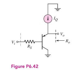
For the ac equivalent circuit in Figure P6.42, \(R_{S}=1 \mathrm{k} \Omega\) and the transistor parameters are \(\beta=80\) and \(V_{A}=50 \mathrm{~V}\).(a) For \(I_{C Q}=2 \mathrm{~mA}\), find \(A_{v}, R_{i}\), and \(R_{o}\).(b) Repeat part (a) for \(I_{C Q}=0.2 \mathrm{~mA}\). Ro V www Rs Figure
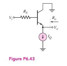
The circuit and transistor parameters for the ac equivalent circuit in Figure P6.43 are \(R_{S}=0.5 \mathrm{k} \Omega, \beta=120\), and \(V_{A}=\infty\). (a) Determine the required value of \(I_{Q}\) to produce a small-signal output resistance of \(R_{o}=15 \Omega\). (b) Using the results of part
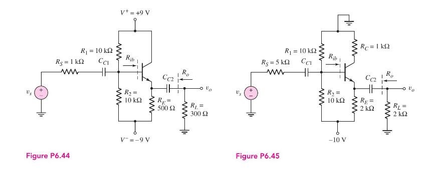
The transistor parameters for the circuit in Figure P6.44 are \(\beta=180\) and \(V_{A}=\infty\). (a) Find \(I_{C Q}\) and \(V_{C E Q}\). (b) Plot the dc and ac load lines. (c) Calculate the small-signal voltage gain. (d) Determine the input and output resistances \(R_{i b}\) and \(R_{o}\). R = 1
Consider the circuit in Figure P6.45. The transistor parameters are \(\beta=120\) and \(V_{A}=\infty\). Repeat parts (a)-(d) of Problem 6.44.Data From Problem 6.44:-The transistor parameters for the circuit in Figure P6.44 are \(\beta=180\) and \(V_{A}=\infty\).(a) Find \(I_{C Q}\) and \(V_{C E
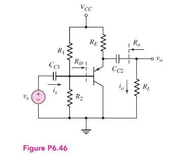
For the circuit shown in Figure P6.46, let \(V_{C C}=3.3 \mathrm{~V}, R_{L}=4 \mathrm{k} \Omega\), \(R_{1}=585 \mathrm{k} \Omega, R_{2}=135 \mathrm{k} \Omega\), and \(R_{E}=12 \mathrm{k} \Omega\). The transistor parameters are \(\beta=90\) and \(V_{A}=60 \mathrm{~V}\). (a) Determine the quiescent
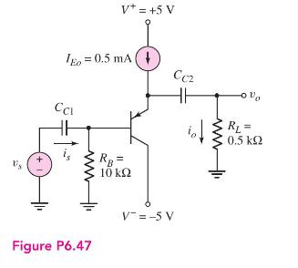
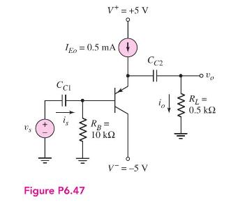
For the transistor in Figure P6.47, \(\beta=80\) and \(V_{A}=150\) V.(a) Determine the dc voltages at the base and emitter terminals.(b) Calculate the smallsignal parameters \(g_{m}, r_{\pi}\), and \(r_{o}\).(c) Determine the small-signal voltage gain and current gain.(d) Repeat part (c) if a \(2
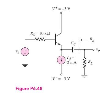
Consider the emitter-follower amplifier shown in Figure P6.48. The transistor parameters are \(\beta=100\) and \(V_{A}=100 \mathrm{~V}\). (a) Find the output resistance \(R_{o}\). (b) Determine the small-signal voltage gain for (i) \(R_{L}=500 \Omega\) and (ii) \(R_{L}=5 \mathrm{k} \Omega\). +-
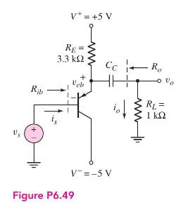
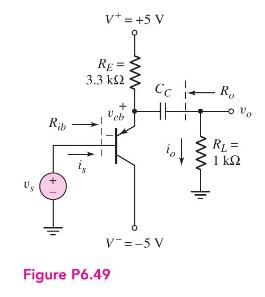
The transistor parameters for the circuit in Figure P6.49 are \(\beta=110\), \(V_{A}=50 \mathrm{~V}\), and \(V_{E B}\) (on) \(=0.7 \mathrm{~V}\). (a) Determine the quiescent values \(I_{C Q}\) and \(V_{E C Q}\). (b) Find \(A_{v}, R_{i b}\), and \(R_{o}\). (c) The signal source is \(v_{s}(t)=2.8
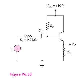
For the transistor in Figure P6.50, the parameters are \(\beta=100\) and \(V_{A}=\infty\). (a) Design the circuit such that \(I_{E Q}=1 \mathrm{~mA}\) and the \(Q\)-point is in the center of the dc load line. (b) If the peak-to-peak sinusoidal output voltage is 4 \(\mathrm{V}\), determine the
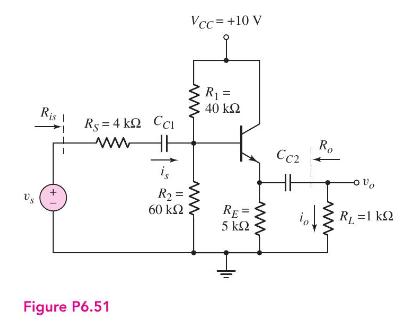
In the circuit shown in Figure P6.51, determine the range in small-signal voltage gain \(A_{v}=v_{o} / v_{s}\) and current gain \(A_{i}=i_{o} / i_{s}\) if \(\beta\) is in the range \(75 \leq \beta \leq 150\). Vcc +10 V Ris Rs = 4kQ CCl www HH 1 +1 Figure P6.51 R = 40 K CC2 ww is R = 60 RE 5 Ro R
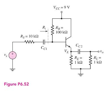
The transistor current gain \(\beta\) in the circuit shown in Figure \(\mathrm{P} 6.52\) is in the range \(50 \leq \beta \leq 200\). (a) Determine the range in the dc values of \(I_{E}\) and \(V_{E}\). (b) Determine the range in the values of input resistance \(R_{i}\) and voltage gain
Consider the circuit shown in Figure P6.47. The transistor current gain is in the range \(100 \leq \beta \leq 180\) and the Early voltage is \(V_{A}=150 \mathrm{~V}\). Determine the range in small-signal voltage gain if the load resistance varies from \(R_{L}=0.5 \mathrm{k} \Omega\) to \(R_{L}=500
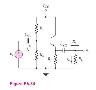
For the circuit in Figure P6.54, the parameters are \(V_{C C}=5 \mathrm{~V}\) and \(R_{E}=500 \Omega\). The transistor parameters are \(\beta=120\) and \(V_{A}=\infty\). (a) Design the circuit to obtain a small-signal current gain of \(A_{i}=i_{o} / i_{s}=10\) for \(R_{L}=500 \Omega\). Find
Design an emitter-follower circuit with the configuration shown in Figure 6.49 such that the input resistance \(R_{i}\), as defined in Figure 6.51, is \(120 \mathrm{k} \Omega\). Assume transistor parameters of \(\beta=120\) and \(V_{A}=\infty\). Let \(V_{C C}=5 \mathrm{~V}\) and \(R_{E}=2
(a) For the emitter-follower circuit in Figure P6.54, assume \(V_{C C}=24 \mathrm{~V}\), \(\beta=75\), and \(A_{i}=i_{o} / i_{s}=8\). Design the circuit to drive an \(8 \Omega\) load. (b) Determine the maximum undistorted swing in the output voltage. (c) Determine the output resistance \(R_{o}\).
The output of an amplifier can be represented by \(v_{s}=4 \sin \omega t(\mathrm{~V})\) and \(R_{S}=4 \mathrm{k} \Omega\). An emitter-follower circuit, with the configuration shown in Figure 6.54, is to be designed such that the output signal does not vary by more than 5 percent when a load in the
An emitter-follower amplifier, with the configuration shown in Figure 6.54, is to be designed such that an audio signal given by \(v_{s}=5 \sin (3000 t) \mathrm{V}\) but with a source resistance of \(R_{S}=10 \mathrm{k} \Omega\) can drive a small speaker. Assume the supply voltages are \(V^{+}=+12
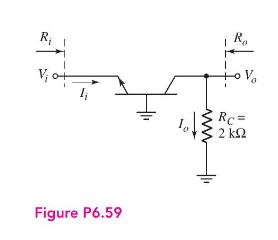
Figure P6.59 is an ac equivalent circuit of a common-base amplifier. The transistor parameters are \(\beta=120, V_{A}=\infty\), and \(I_{C Q}=1 \mathrm{~mA}\). Determine (a) the voltage gain \(A_{v}=V_{o} / V_{i}\), (b) the current gain \(A_{i}=I_{o} / I_{i}\), (c) the input resistance \(R_{i}\),
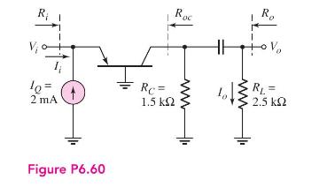
The transistor in the ac equivalent circuit shown in Figure P6.60 has parameters \(\beta=80\) and \(V_{A}=\infty\). Determine (a) the voltage gain \(A_{v}=V_{o} / V_{i}\), (b) the current gain \(A_{i}=I_{o} / I_{i}\), and (c) the input resistance \(R_{i}\). (d) If \(V_{A}=80 \mathrm{~V}\), find (i)
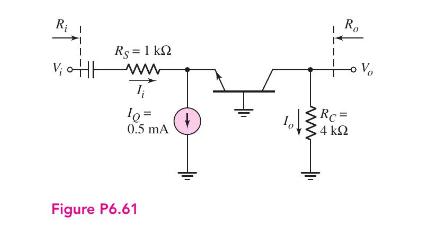
Consider the ac equivalent common-base circuit shown in Figure P6.61. The transistor has parameters \(\beta=110\) and \(V_{A}=\infty\). Determine (a) the voltage gain \(A_{v}=V_{o} / V_{i}\), (b) the current gain \(A_{i}=I_{o} / I_{i}\), (c) the input resistance \(R_{i}\), and (d) the output
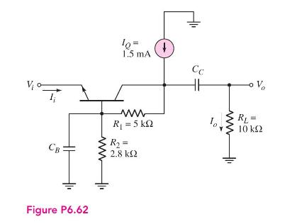
Figure P6.62 shows an ac equivalent circuit of a common-base amplifier. The parameters of the transistor are \(\beta=120, V_{B E}(\mathrm{on})=0.7 \mathrm{~V}\), and \(V_{A}=\infty\). (a) Determine the quiescent values \(I_{C Q}\) and \(V_{C E Q}\). (b) Find the small-signal voltage gain
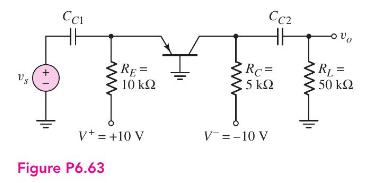
The transistor in the circuit shown in Figure P6.63 has \(\beta=100\) and \(V_{A}=\infty\). (a) Determine the quiescent values \(I_{C Q}\) and \(V_{E C Q}\). (b) Determine the small-signal voltage gain \(A_{v}=v_{o} / v_{s}\). CCI RE= 10 CC2 RC= 15 V+=+10 V V=-10 V Figure P6.63 ww RL= 50
Repeat Problem 6.63 with a \(100 \Omega\) resistor in series with the \(v_{s}\) signal source.Data From Problem 6.63:-The transistor in the circuit shown in Figure P6.63 has \(\beta=100\) and \(V_{A}=\infty\). (a) Determine the quiescent values \(I_{C Q}\) and \(V_{E C Q}\). (b) Determine the
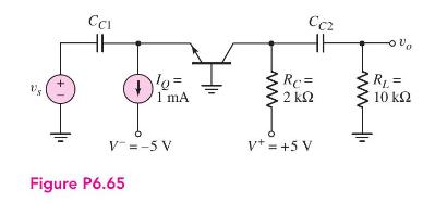
Consider the common-base circuit in Figure P6.65. The transistor has parameters \(\beta=120\) and \(V_{A}=\infty\). (a) Determine the quiescent \(V_{C E Q}\). (b) Determine the small-signal voltage gain \(A_{v}=v_{o} / v_{s}\). 's CCI HH 10= D'MA 1 mA www Rc= 2 CC2 HH RL R = 10 V=-5 V V+=+5 V
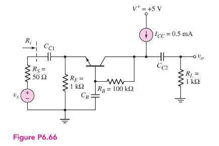
For the circuit shown in Figure P6.66, the transistor parameters are \(\beta=100\) and \(V_{A}=\infty\). (a) Determine the dc voltages at the collector, base, and emitter terminals. (b) Determine the small-signal voltage gain \(A_{v}=v_{o} / v_{s}\). (c) Find the input resistance \(R_{i}\). V+=+5 V
Showing 1000 - 1100
of 4723
First
4
5
6
7
8
9
10
11
12
13
14
15
16
17
18
Last
Step by Step Answers