New Semester
Started
Get
50% OFF
Study Help!
--h --m --s
Claim Now
Question Answers
Textbooks
Find textbooks, questions and answers
Oops, something went wrong!
Change your search query and then try again
S
Books
FREE
Study Help
Expert Questions
Accounting
General Management
Mathematics
Finance
Organizational Behaviour
Law
Physics
Operating System
Management Leadership
Sociology
Programming
Marketing
Database
Computer Network
Economics
Textbooks Solutions
Accounting
Managerial Accounting
Management Leadership
Cost Accounting
Statistics
Business Law
Corporate Finance
Finance
Economics
Auditing
Tutors
Online Tutors
Find a Tutor
Hire a Tutor
Become a Tutor
AI Tutor
AI Study Planner
NEW
Sell Books
Search
Search
Sign In
Register
study help
computer science
systems analysis and design 12th
Microelectronics Circuit Analysis And Design 4th Edition Donald A. Neamen - Solutions
Describe the piecewise linear model of a diode and why it is useful. What is the diode turn-on voltage?
Define a load line in a simple diode circuit.
Under what conditions is the small-signal model of a diode used in the analysis of a diode circuit?
Describe the operation of a simple solar cell circuit.
How do the \(i-v\) characteristics of a Schottky barrier diode differ from those of a pn junction diode?
What characteristic of a Zener diode is used in the design of a Zener diode circuit?
Describe the characteristics of a photodiode and a photodiode circuit.
(a) Calculate the intrinsic carrier concentration in silicon at (i) \(T=250 \mathrm{~K}\) and (ii) \(T=350 \mathrm{~K}\).(b) Repeat part (a) for gallium arsenide.
(a) The intrinsic carrier concentration in silicon is to be no larger than \(n_{i}=10^{12} \mathrm{~cm}^{-3}\). Determine the maximum allowable temperature.(b) Repeat part (a) for \(n_{i}=10^{9} \mathrm{~cm}^{-3}\).
Calculate the intrinsic carrier concentration in silicon and germanium at (a) \(T=100 \mathrm{~K}\), (b) \(T=300 \mathrm{~K}\), and (c) \(T=500 \mathrm{~K}\).
(a) Find the concentration of electrons and holes in a sample of germanium that has a concentration of donor atoms equal to \(10^{15} \mathrm{~cm}^{-3}\). Is the semiconductor n-type or p-type?(b) Repeat part (a) for silicon.
Gallium arsenide is doped with acceptor impurity atoms at a concentration of \(10^{16} \mathrm{~cm}^{-3}\).(a) Find the concentration of electrons and holes. Is the semiconductor n-type or p-type?(b) Repeat part (a) for germanium.
Silicon is doped with \(5 \times 10^{16}\) arsenic atoms \(/ \mathrm{cm}^{3}\).(a) Is the material \(\mathrm{n}\) - or p-type?(b) Calculate the electron and hole concentrations at \(T=300 \mathrm{~K}\).(c) Repeat part (b) for \(T=350 \mathrm{~K}\).
(a) Calculate the concentration of electrons and holes in silicon that has a concentration of acceptor atoms equal to \(5 \times 10^{16} \mathrm{~cm}^{-3}\). Is the semiconductor n-type or p-type?(b) Repeat part (a) for GaAs.
A silicon sample is fabricated such that the hole concentration is \(p_{o}=2 \times 10^{17} \mathrm{~cm}^{-3}\). (a) Should boron or arsenic atoms be added to the intrinsic silicon? (b) What concentration of impurity atoms must be added? (c) What is the concentration of electrons?
The electron concentration in silicon at \(T=300 \mathrm{~K}\) is \(n_{o}=5 \times 10^{15} \mathrm{~cm}^{-3}\).(a) Determine the hole concentration. (b) Is the material n-type or p-type?(c) What is the impurity doping concentration?
(a) A silicon semiconductor material is to be designed such that the majority carrier electron concentration is \(n_{o}=7 \times 10^{15} \mathrm{~cm}^{-3}\). Should donor or acceptor impurity atoms be added to intrinsic silicon to achieve this electron concentration? What concentration of dopant
(a) The applied electric field in p-type silicon is \(E=10 \mathrm{~V} / \mathrm{cm}\). The semiconductor conductivity is \(\sigma=1.5(\Omega-\mathrm{cm})^{-1}\) and the cross-sectional area is \(A=10^{-5} \mathrm{~cm}^{2}\). Determine the drift current. (b) The cross-sectional area of a
A drift current density of \(120 \mathrm{~A} / \mathrm{cm}^{2}\) is established in n-type silicon with an applied electric field of \(18 \mathrm{~V} / \mathrm{cm}\). If the electron and hole mobilities are \(\mu_{n}=1250 \mathrm{~cm}^{2} / \mathrm{V}-\mathrm{s}\) and \(\mu_{p}=450 \mathrm{~cm}^{2}
An n-type silicon material has a resistivity of \(ho=0.65 \Omega-\mathrm{cm}\). (a) If the electron mobility is \(\mu_{n}=1250 \mathrm{~cm}^{2} / \mathrm{V}-\mathrm{s}\), what is the concentration of donor atoms? (b) Determine the required electric field to establish a drift current density of
(a) The required conductivity of a silicon material must be \(\sigma=1.5(\Omega-\mathrm{cm})^{-1}\). If \(\mu_{n}=1000 \mathrm{~cm}^{2} / \mathrm{V}-\mathrm{s}\) and \(\mu_{p}=375 \mathrm{~cm}^{2} / \mathrm{V}-\mathrm{s}\), what concentration of donor atoms must be added? (b) The required
In GaAs, the mobilities are \(\mu_{n}=8500 \mathrm{~cm}^{2} / \mathrm{V}-\mathrm{s}\) and \(\mu_{p}=400 \mathrm{~cm}^{2} / \mathrm{V}-\mathrm{s}\). (a) Determine the range in conductivity for a range in donor concentration of \(10^{15} \leq N_{d} \leq 10^{19} \mathrm{~cm}^{-3}\). (b) Using the
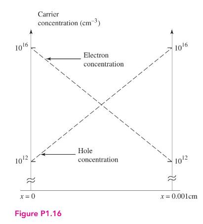
The electron and hole concentrations in a sample of silicon are shown in Figure P1.16. Assume the electron and hole mobilities are the same as in Problem 1.12. Determine the total diffusion current density versus distance \(x\) for \(0 \leq x \leq 0.001\mathrm{~cm}\).Data From Problem 1.12:-A drift
The hole concentration in silicon is given by\[p(x)=10^{4}+10^{15} \exp \left(-x / L_{p}\right) \quad x \geq 0\]The value of \(L_{p}\) is \(10 \mu \mathrm{m}\). The hole diffusion coefficient is \(D_{p}=15 \mathrm{~cm}^{2} / \mathrm{s}\). Determine the hole diffusion current density at (a) \(x=0\),
GaAs is doped to \(N_{a}=10^{17} \mathrm{~cm}^{-3}\). (a) Calculate \(n_{o}\) and \(p_{o}\). (b) Excess electrons and holes are generated such that \(\delta n=\delta p=10^{15} \mathrm{~cm}^{-3}\). Determine the total concentration of electrons and holes.
Consider a silicon pn junction. The \(\mathrm{n}\)-region is doped to a value of \(N_{d}=10^{16} \mathrm{~cm}^{-3}\). The built-in potential barrier is to be \(V_{b i}=0.712 \mathrm{~V}\). Determine the required p-type doping concentration.
The donor concentration in the n-region of a silicon pn junction is \(N_{d}=10^{16} \mathrm{~cm}^{-3}\). Plot \(V_{b i}\) versus \(N_{a}\) over the range \(10^{15} \leq N_{a} \leq 10^{18} \mathrm{~cm}^{-3}\) where \(N_{a}\) is the acceptor concentration in the p-region.
Consider a uniformly doped \(\mathrm{GaAs}\) pn junction with doping concentrations of \(N_{a}=5 \times 10^{18} \mathrm{~cm}^{-3}\) and \(N_{d}=5 \times 10^{16} \mathrm{~cm}^{-3}\). Plot the built-in potential barrier \(V_{b i}\) versus temperature for \(200 \mathrm{~K} \leq T \leq 500
The zero-biased junction capacitance of a silicon pn junction is \(C_{j o}=0.4 \mathrm{pF}\). The doping concentrations are \(N_{a}=1.5 \times 10^{16} \mathrm{~cm}^{-3}\) and \(N_{d}=4 \times 10^{15} \mathrm{~cm}^{-3}\). Determine the junction capacitance at (a) \(V_{R}=1 \mathrm{~V}\), (b)
The zero-bias capacitance of a silicon pn junction diode is \(C_{j o}=0.02 \mathrm{pF}\) and the built-in potential is \(V_{b i}=0.80 \mathrm{~V}\). The diode is reverse biased through a \(47-\mathrm{k} \Omega\) resistor and a voltage source.(a) For \(t
The doping concentrations in a silicon pn junction are \(N_{d}=5 \times 10^{15} \mathrm{~cm}^{-3}\) and \(N_{a}=10^{17} \mathrm{~cm}^{-3}\). The zero-bias junction capacitance is \(C_{j o}=0.60 \mathrm{pF}\). An inductance of \(1.50 \mathrm{mH}\) is connected in parallel with the pn junction.
(a) At what reverse-bias voltage does the reverse-bias current in a silicon pn junction diode reach 90 percent of its saturation value? (b) What is the ratio of the current for a forward-bias voltage of \(0.2 \mathrm{~V}\) to the current for a reversebias voltage of \(0.2 \mathrm{~V}\) ?
(a) The reverse-saturation current of a pn junction diode is \(I_{S}=10^{-11} \mathrm{~A}\). Determine the diode voltage to produce currents of (i) \(10 \mu \mathrm{A}, 100 \mu \mathrm{A}\), \(1 \mathrm{~mA}\), and (ii) \(-5 \times 10^{-12} \mathrm{~A}\).(b) Repeat part (a) for \(I_{S}=10^{-13}
Plot \(\log _{10} I_{D}\) versus \(V_{D}\) over the range \(0.1 \leq V_{D} \leq 0.7\mathrm{~V}\) for (a) \(I_{S}=\) \(10^{-12}\) and (b) \(I_{S}=10^{-14} \mathrm{~A}\).
A pn junction diode has \(I_{S}=2 \mathrm{nA}\). (a) Determine the diode voltage if (i) \(I_{D}=2 \mathrm{~A}\) and (ii) \(I_{D}=20 \mathrm{~A}\). (b) Determine the diode current if (i) \(V_{D}=0.4 \mathrm{~V}\) and (ii) \(V_{D}=0.65 \mathrm{~V}\).
(a) A germanium pn junction has a diode current of \(I_{D}=1.5 \mathrm{~mA}\) when biased at \(V_{D}=0.30 \mathrm{~V}\). What is the reverse-bias saturation current? (b) Using the results of part (a), determine the diode current when the diode is biased at (i) \(V_{D}=0.35 \mathrm{~V}\) and (ii)
The reverse-saturation current of a silicon pn junction diode at \(T=300 \mathrm{~K}\) is \(I_{S}=10^{-12} \mathrm{~A}\). Determine the temperature range over which \(I_{S}\) varies from \(0.5 \times 10^{-12} \mathrm{~A}\) to \(50 \times 10^{-12} \mathrm{~A}\).
A pn junction diode is in series with a \(1 \mathrm{M} \Omega\) resistor and a \(2.8 \mathrm{~V}\) power supply. The reverse-saturation current of the diode is \(I_{S}=5 \times 10^{-11} \mathrm{~A}\).(a) Determine the diode current and voltage if the diode is forward biased.(b) Repeat part (a) if
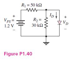
The diode in the circuit shown in Figure P1.40 has a reverse-saturation current of \(I_{S}=5 \times 10^{-13} \mathrm{~A}\). Determine the diode voltage and current.Figure P1.40:- + VPS= 1.2 V R = 50 k ww R = 30 ID Figure P1.40 + VD
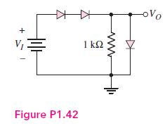
(a) The reverse-saturation current of each diode in the circuit shown in Figure P1.42 is \(I_{S}=6 \times 10^{-14} \mathrm{~A}\). Determine the input voltage \(V_{I}\) required to produce an output voltage of \(V_{O}=0.635 \mathrm{~V}\).(b) Repeat part (a) if the \(1 \mathrm{k} \Omega\) resistor is
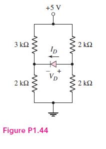
Consider the circuit shown in Figure P1.44. Determine the diode current \(I_{D}\) and diode voltage \(V_{D}\) for (a) \(V_{\gamma}=0.6 \mathrm{~V}\) and (b) \(V_{\gamma}=0.7 \mathrm{~V}\).Figure P1.44:- 3 2 +5 V ww ww 51415 VD Figure P1.44 + ww 2 2
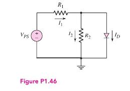
The cut-in voltage of the diode shown in the circuit in Figure P1.46 is \(V_{\gamma}=0.7 \mathrm{~V}\). The diode is to remain biased "on" for a power supply voltage in the range \(5 \leq V_{P S} \leq 10 \mathrm{~V}\). The minimum diode current is to be \(I_{D}(\mathrm{~min})=2 \mathrm{~mA}\). The
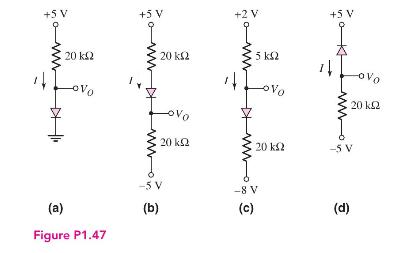
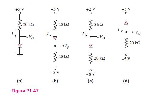
Repeat Problem 1.47 if the reverse-saturation current for each diode is \(I_{S}=5 \times 10^{-14} \mathrm{~A}\). What is the voltage across each diode?Data From Problem 1.47:-Find \(I\) and \(V_{O}\) in each circuit shown in Figure P1.47 if (i) \(V_{\gamma}=0.7 \mathrm{~V}\) and (ii)
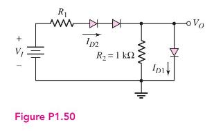
Assume each diode in the circuit shown in Figure P1.50 has a cut-in voltage of \(V_{\gamma}=0.65 \mathrm{~V}\). (a) The input voltage is \(V_{I}=5 \mathrm{~V}\). Determine the value of \(R_{1}\) required such that \(I_{D 1}\) is one-half the value of \(I_{D 2}\). What are the values of \(I_{D 1}\)
Determine the small-signal diffusion resistance \(r_{d}\) for a diode biased at (a) \(I_{D}=26 \mu \mathrm{A}\), (b) \(I_{D}=260 \mu \mathrm{A}\), and (c) \(I_{D}=2.6 \mathrm{~mA}\).
The forward-bias currents in a pn junction diode and a Schottky diode are \(0.72 \mathrm{~mA}\). The reverse-saturation currents are \(I_{S}=5 \times 10^{-13} \mathrm{~A}\) and \(I_{S}=5 \times 10^{-8} \mathrm{~A}\), respectively. Determine the forward-bias voltage across each diode.
The reverse-saturation currents of a Schottky diode and a pn junction diode are \(I_{S}=5 \times 10^{-8} \mathrm{~A}\) and \(10^{-12} \mathrm{~A}\), respectively.(a) The diodes are connected in parallel and the parallel combination is driven by a constant current of \(0.5 \mathrm{~mA}\). (i)
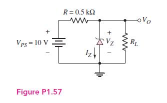
(a) The Zener diode in Figure P1.57 is ideal with \(V_{Z}=6.8\) V. Determine the maximum current and maximum power dissipated in the diode \(\left(R_{L}=\infty\right)\). (b) Determine the value of \(R_{L}\) such that \(I_{Z}\) is reduced to 0.1 of its maximum value.Figure P1.57:- Vps = 10 V +
The output current of a pn junction diode used as a solar cell can be given by\[I_{D}=0.2-5 \times 10^{-14}\left[\exp \left(\frac{V_{D}}{V_{T}}\right)-1\right] \quad \mathrm{A}\]The short-circuit current is defined as \(I_{S C}=I_{D}\) when \(V_{D}=0\) and the opencircuit voltage is defined as
Using the current-voltage characteristics of the solar cell described in Problem 1.60, plot \(I_{D}\) versus \(V_{D}\).Data From Problem 1.60:-The output current of a pn junction diode used as a solar cell can be given by \[I_{D}=0.2-5 \times 10^{-14}\left[\exp
(a) Using the current-voltage characteristics of the solar cell described in problem 1.60, determine \(V_{D}\) when \(I_{D}=0.8 I_{S C}\). (b) Using the results of part (a), determine the power supplied by the solar cell.Data From Problem 1.60:-The output current of a pn junction diode used as a
Use a computer simulation to generate the ideal current-voltage characteristics of a diode from a reverse-bias voltage of \(5 \mathrm{~V}\) to a forward-bias current of \(1 \mathrm{~mA}\), for an \(I_{S}\) parameter value of (a) \(10^{-15} \mathrm{~A}\) and (b) \(10^{-13} \mathrm{~A}\). Use the
Use a computer simulation to find the diode current and voltage for the circuit described in Problem 1.38.Data From Problem 1.38:-A pn junction diode is in series with a \(1 \mathrm{M} \Omega\) resistor and a \(2.8 \mathrm{~V}\) power supply. The reverse-saturation current of the diode is \(I_{S}=5
The reverse-saturation current for each diode in Figure P1.42 is \(I_{S}=10^{-14} \mathrm{~A}\). Use a computer simulation to plot the output voltage \(V_{O}\) versus the input voltage \(V_{I}\) over the range \(0 \leq V_{I} \leq 2.0\mathrm{~V}\).Figure P1.42:- + D 1k2 Figure P1.42 ww -oVo
Use a computer simulation to find the diode current, diode voltage, and output voltage for each circuit shown in Figure P1.47. Assume \(I_{S}=10^{-13} \mathrm{~A}\) for each diode.Figure P1.47:- +5 V +5 V +2 V +5V ww 20 Vo 20 (a) Figure P1.47 www ovo 20 5 -5 V (b) ww 5 Vo OVO 20 20 -5 V -8 V
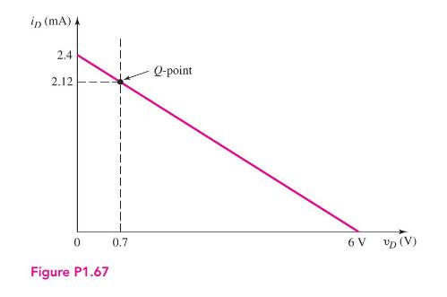
Design a diode circuit to produce the load line and \(Q\)-point shown in Figure P1.67. Assume diode piecewise linear parameters of \(V_{\gamma}=0.7 \mathrm{~V}\) and \(r_{f}=0\). in (mA) 2.4 Q-point 2.12 0 Figure P1.67 0.7 6 V VD (V)
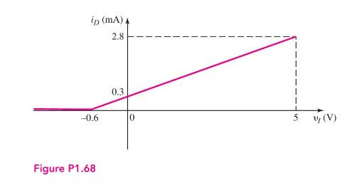
Design a circuit to produce the characteristics shown in Figure P1.68, where \(i_{D}\) is the diode current and \(v_{I}\) is the input voltage. Assume diode piecewise linear parameters of \(V_{\gamma}=0.7 \mathrm{~V}\) and \(r_{f}=0\). ip (mA) 2.8 0.3 -0.6 0 5 v, (V) Figure P1.68
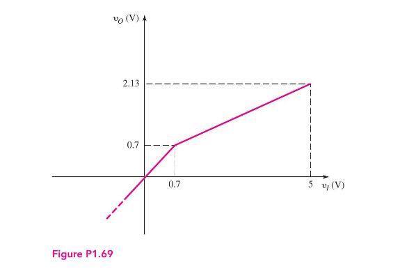
Design a circuit to produce the characteristics shown in Figure P1.69, where \(v_{O}\) is the output voltage and \(v_{I}\) is the input voltage. Assume diode piecewise linear parameters of \(V_{\gamma}=0.7 \mathrm{~V}\) and \(r_{f}=0\). Figure P1.69 vo (V) 2.13 0.7 0.7 5 v,(V)
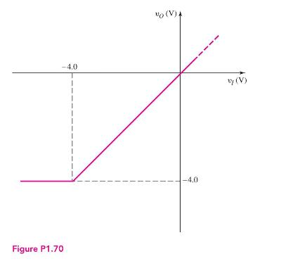
Design a circuit to produce the characteristics shown in Figure P1.70, where \(v_{O}\) is the output voltage and \(v_{I}\) is the input voltage. Assume diode piecewise linear parameters of \(V_{\gamma}=0.7 \mathrm{~V}\) and \(r_{f}=0\). Figure P1.70 -4.0 vo (V). -4.0 vy (V)
What characteristic of a diode is used in the design of diode signal processing circuits?
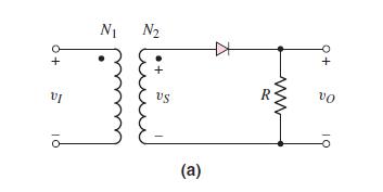
Describe a simple half-wave diode rectifier circuit and sketch the output voltage versus time.
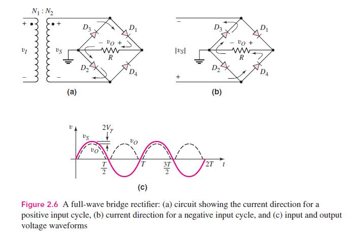
Describe a simple full-wave diode rectifier circuit and sketch the output voltage versus time.
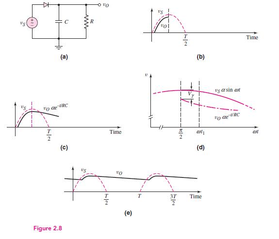
What is the advantage of connecting an \(R C\) filter to the output of a diode rectifier circuit?
Define ripple voltage. How can the magnitude of the ripple voltage be reduced?
Describe a simple Zener diode voltage reference circuit.
What effect does the Zener diode resistance have on the voltage reference circuit operation? Define load regulation.
What are the general characteristics of diode clipper circuits?
Describe a simple diode clipper circuit that limits the negative portion of a sinusoidal input voltage to a specified value.
What are the general characteristics of diode clamper circuits?
What one circuit element, besides a diode, is present in all diode clamper circuits?
Describe the procedure used in the analysis of a circuit containing two diodes. How many initial assumptions concerning the state of the circuit are possible?
Describe a diode OR logic circuit. Compare a logic 1 value at the output compared to a logic 1 value at the input. Are they the same value?
Describe a diode AND logic circuit. Compare a logic 0 value at the output compared to a logic 0 value at the input. Are they the same value?
Describe a simple circuit that can be used to turn an LED on or off with a high or low input voltage.
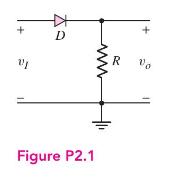
Consider the circuit shown in Figure P2.1. Let \(R=1 \mathrm{k} \Omega, V_{\gamma}=0.6 \mathrm{~V}\), and \(r_{f}=20 \Omega\). (a) Plot the voltage transfer characteristics \(v_{O}\) versus \(v_{I}\) over the range \(-10 \leq v_{I} \leq 10 \mathrm{~V}\). (b) Assume \(v_{I}=10 \sin \omega
For the circuit shown in Figure P2.1, show that for \(v_{I} \geq 0\), the output voltage is approximately given byFigure P2.1 \(v_{O}=v_{I}-V_{T} \ln \left(\frac{v_{O}}{I_{S} R}\right)\) + D ww + R Vo Figure P2.1
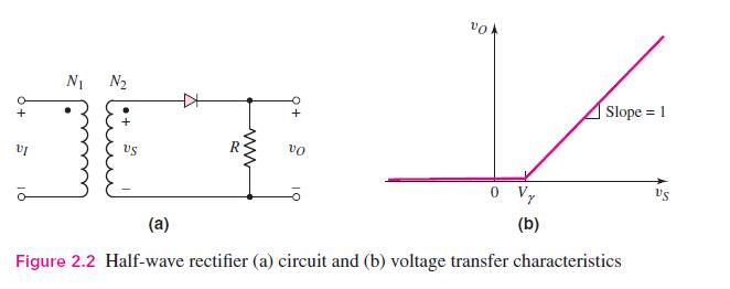
A half-wave rectifier such as shown in Figure 2.2 (a) has a \(2 \mathrm{k} \Omega\) load. The input is a \(120 \mathrm{~V}(\mathrm{rms}), 60 \mathrm{~Hz}\) signal and the transformer is a 10:1 stepdown transformer. The diode has a cut-in voltage of \(V_{\gamma}=0.7
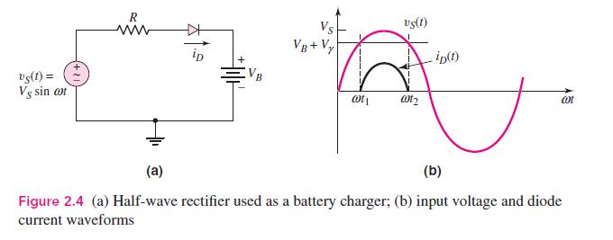
Consider the battery charging circuit shown in Figure 2.4(a). Assume that \(V_{B}=9 \mathrm{~V}, V_{S}=15 \mathrm{~V}\), and \(\omega=2 \pi(60)\). (a) Determine the value of \(R\) such that the average battery charging current is \(i_{D}=0.8 \mathrm{~A}\). (b) Find the fraction of time that the
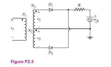
Figure P2.5 shows a simple full-wave battery charging circuit. Assume \(V_{B}=9 \mathrm{~V}, V_{\gamma}=0.7 \mathrm{~V}\), and \(v_{S}=15 \sin [2 \pi(60) t]\) (V). (a) Determine \(R\) such that the peak battery charging current is 1.2A. (b) Determine the average battery charging current. (c)
The full-wave rectifier circuit shown in Figure 2.5 (a) in the text is to deliver \(0.2 \mathrm{~A}\) and \(12 \mathrm{~V}\) (peak values) to a load. The ripple voltage is to be limited to \(0.25 \mathrm{~V}\). The input signal is \(120 \mathrm{~V}\) (rms) at \(60 \mathrm{~Hz}\). Assume diode
The input signal voltage to the full-wave rectifier circuit in Figure 2.6 (a) in the text is \(v_{I}=160 \sin [2 \pi(60) t] \mathrm{V}\). Assume \(V_{\gamma}=0.7 \mathrm{~V}\) for each diode. Determine the required turns ratio of the transformer to produce a peak output voltage of (a) \(25
The output resistance of the full-wave rectifier in Figure 2.6(a) in the text is \(R=150 \Omega\). A filter capacitor is connected in parallel with \(R\). Assume \(V_{\gamma}=0.7 \mathrm{~V}\). The peak output voltage is to be \(12 \mathrm{~V}\) and the ripple voltage is to be no more than \(0.3
Repeat Problem 2.8 for the half-wave rectifier in Figure 2.2(a).Data From Problem 2.8:-The output resistance of the full-wave rectifier in Figure 2.6 (a) in the text is \(R=150 \Omega\). A filter capacitor is connected in parallel with \(R\). Assume \(V_{\gamma}=0.7 \mathrm{~V}\). The peak output
Consider the half-wave rectifier circuit shown in Figure 2.8 (a) in the text. Assume \(v_{S}=10 \sin [2 \pi(60) t](\mathrm{V}), V_{\gamma}=0.7 \mathrm{~V}\), and \(R=500 \Omega\).(a) What is the peak output voltage?(b) Determine the value of capacitance required such that the ripple voltage is no
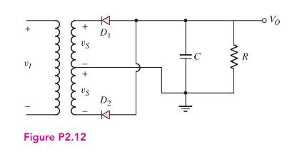
The full-wave rectifier circuit shown in Figure P2.12 has an input signal whose frequency is \(60 \mathrm{~Hz}\). The rms value of \(v_{S}=8.5 \mathrm{~V}\). Assume each diode cut-in voltage is \(V_{\gamma}=0.7 \mathrm{~V}\). (a) What is the maximum value of \(V_{O}\) ? (b) If \(R=10 \Omega\),
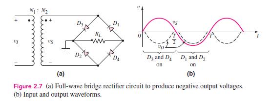
Consider the full-wave rectifier circuit in Figure 2.7 of the text. The output resistance is \(R_{L}=125 \Omega\), each diode cut-in voltage is \(V_{\gamma}=0.7 \mathrm{~V}\), and the frequency of the input signal is \(60 \mathrm{~Hz}\). A filter capacitor is connected in parallel with \(R_{L}\).
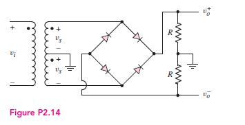
The circuit in Figure P2.14 is a complementary output rectifier. If \(v_{s}=26\) \(\sin [2 \pi(60) t] \mathrm{V}\), sketch the output waveforms \(v_{o}^{+}\)and \(v_{o}^{-}\)versus time, assuming \(V_{\gamma}=0.6 \mathrm{~V}\) for each diode.Figure P2.14:- Figure P2.14 www R R
A full-wave rectifier is to be designed using the center-tapped transformer configuration. The peak output voltage is to be \(12 \mathrm{~V}\), the nominal load current is to be \(0.5 \mathrm{~A}\), and the ripple voltage is to be limited to 3 percent. Assume \(V_{\gamma}=0.8 \mathrm{~V}\) and let
A full-wave rectifier is to be designed using the bridge circuit configuration. The peak output voltage is to be \(9 \mathrm{~V}\), the nominal load current is to be 100 \(\mathrm{mA}\), and the ripple voltage is to be limited to \(V_{r}=0.2 \mathrm{~V}\). Assume \(V_{\gamma}=0.8 \mathrm{~V}\) and
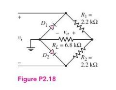
(a) Sketch \(v_{o}\) versus time for the circuit in Figure P2.18. The input is a sine wave given by \(v_{i}=10 \sin \omega t \mathrm{~V}\). Assume \(V_{\gamma}=0\). (b) Determine the rms value of the output voltage. www RL=6.8 k R = 2.2 Figure P2.18 R = 2.2
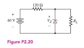
Consider the Zener diode circuit shown in Figure P2.20. Assume \(V_{Z}=12 \mathrm{~V}\) and \(r_{z}=0\). (a) Calculate the Zener diode current and the power dissipated in the Zener diode for \(R_{L}=\infty\). (b) What is the value of \(R_{L}\) such that the current in the Zener diode is one-tenth
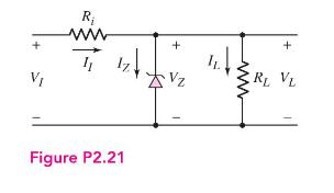
In the voltage regulator circuit in Figure P2.21, \(V_{I}=20 \mathrm{~V}, V_{Z}=10 \mathrm{~V}\), \(R_{i}=222 \Omega\), and \(P_{Z}(\max )=400 \mathrm{~mW}\).(a) Determine \(I_{L}, I_{Z}\), and \(I_{I}\), if \(R_{L}=380 \Omega\).(b) Determine the value of \(R_{L}\) that will establish \(P_{Z}(\max
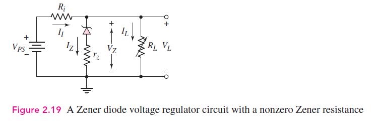
Consider the Zener diode circuit in Figure 2.19 in the text. Assume parameter values of \(V_{Z O}=5.6 \mathrm{~V}\) (diode voltage when \(I_{Z} \cong 0\) ), \(r_{z}=3 \Omega\), and \(R_{i}=50 \Omega\). Determine \(V_{L}, I_{Z}, I_{L}\), and the power dissipated in the diode for (a) \(V_{P S}=10
Design a voltage regulator circuit such as shown in Figure P2.21 so that \(V_{L}=7.5 \mathrm{~V}\). The Zener diode voltage is \(V_{Z}=7.5 \mathrm{~V}\) at \(I_{Z}=10 \mathrm{~mA}\). The incremental diode resistance is \(r_{z}=12 \Omega\). The nominal supply voltage is \(V_{I}=12 \mathrm{~V}\) and
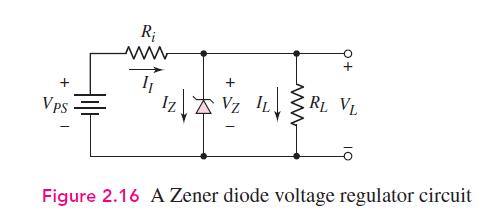
The percent regulation of the Zener diode regulator shown in Figure 2.16 is 5 percent. The Zener voltage is \(V_{Z O}=6 \mathrm{~V}\) and the Zener resistance is \(r_{z}=3 \Omega\). Also, the load resistance varies between 500 and \(1000 \Omega\), the input resistance is \(R_{i}=280 \Omega\), and
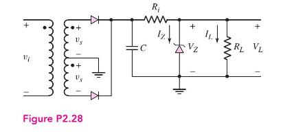
Consider the circuit in Figure P2.28. Let \(V_{\gamma}=0\). The secondary voltage is given by \(v_{s}=V_{s} \sin \omega t\), where \(V_{s}=24 \mathrm{~V}\). The Zener diode has parameters \(V_{Z}=16 \mathrm{~V}\) at \(I_{Z}=40 \mathrm{~mA}\) and \(r_{z}=2 \Omega\). Determine \(R_{i}\) such that the
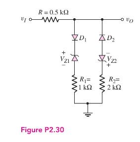
The parameters in the circuit shown in Figure P2.30 are \(V_{\gamma}=0.7 \mathrm{~V}\), \(V_{Z 1}=2.3 \mathrm{~V}\), and \(V_{Z 2}=5.6 \mathrm{~V}\). Plot \(v_{O}\) versus \(v_{I}\) over the range of \(-10 \leq v_{I} \leq+10 \mathrm{~V}\). R = 0.5 k ww + XD Figure P2.30 D - vo R= 1 R= 2
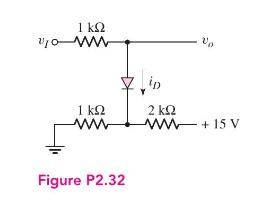
For the circuit in Figure P2.32,(a) plot \(v_{O}\) versus \(v_{I}\) for \(0 \leq v_{I} \leq 15 \mathrm{~V}\). Assume \(V_{\gamma}=0.7 \mathrm{~V}\). Indicate all breakpoints.(b) Plot \(i_{D}\) over the same range of input voltage.(c) Compare the results of parts (a) and (b) with a computer
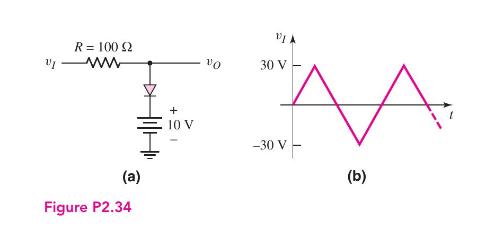
The diode in the circuit of Figure P2.34 (a) has piecewise linear parameters \(V_{\gamma}=0.7 \mathrm{~V}\) and \(r_{f}=10 \Omega\).(a) Plot \(v_{O}\) versus \(v_{I}\) for \(-30 \leq v_{I} \leq 30 \mathrm{~V}\).(b) If the triangular wave, shown in Figure P2.34(b), is applied, plot the output versus
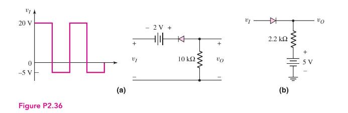
Plot \(v_{O}\) for each circuit in Figure P2.36 for the input shown. Assume (a) \(V_{\gamma}=0\) and (b) \(V_{\gamma}=0.6 \mathrm{~V}\). 20V 0 + Figure P2.36 (a) 2V+ 10k2 + Vo y 2.2 k2 ww (b)
Showing 1500 - 1600
of 4723
First
9
10
11
12
13
14
15
16
17
18
19
20
21
22
23
Last
Step by Step Answers