New Semester
Started
Get
50% OFF
Study Help!
--h --m --s
Claim Now
Question Answers
Textbooks
Find textbooks, questions and answers
Oops, something went wrong!
Change your search query and then try again
S
Books
FREE
Study Help
Expert Questions
Accounting
General Management
Mathematics
Finance
Organizational Behaviour
Law
Physics
Operating System
Management Leadership
Sociology
Programming
Marketing
Database
Computer Network
Economics
Textbooks Solutions
Accounting
Managerial Accounting
Management Leadership
Cost Accounting
Statistics
Business Law
Corporate Finance
Finance
Economics
Auditing
Tutors
Online Tutors
Find a Tutor
Hire a Tutor
Become a Tutor
AI Tutor
AI Study Planner
NEW
Sell Books
Search
Search
Sign In
Register
study help
computer science
systems analysis and design 12th
Microelectronics Circuit Analysis And Design 4th Edition Donald A. Neamen - Solutions
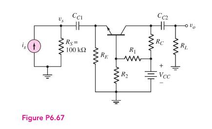
The parameters of the circuit in Figure P6.67 are \(V_{C C}=9 \mathrm{~V}, R_{L}=4 \mathrm{k} \Omega\), \(R_{C}=6 \mathrm{k} \Omega, R_{E}=3 \mathrm{k} \Omega, R_{1}=150 \mathrm{k} \Omega\), and \(R_{2}=50 \mathrm{k} \Omega\). The transistor parameters are \(\beta=125, V_{B E}(\) on \()=0.7
For the common-base circuit shown in Figure P6.67, let \(V_{C C}=5 \mathrm{~V}\), \(R_{L}=12 \mathrm{k} \Omega\), and \(R_{E}=500 \Omega\). The transistor parameters are \(\beta=100\) and \(V_{A}=\infty\). (a) Design the circuit such that the minimum small-signal voltage gain is \(A_{v}=v_{o} /
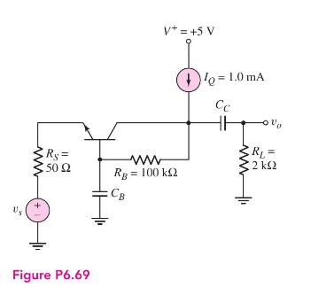
Consider the circuit shown in Figure P6.69. The transistor has parameters \(\beta=60\) and \(V_{A}=\infty\). (a) Determine the quiescent values of \(I_{C Q}\) and \(V_{C E Q}\). (b) Determine the small-signal voltage gain \(A_{v}=v_{o} / v_{s}\). Ry= 150 ww RB = 100 k2 CB Figure P6.69 V+ = +5 V Q
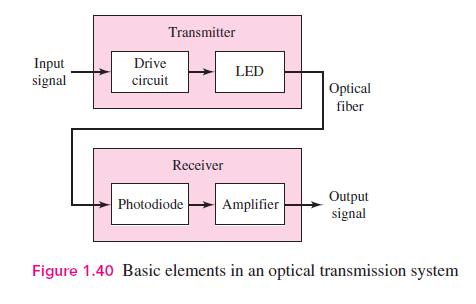
A photodiode in an optical transmission system, such as shown in Figure 1.40, can be modeled as a Norton equivalent circuit with \(i_{s}\) in parallel with \(R_{S}\) as shown in Figure P6.67. Assume that the current source is given by \(i_{s}=2.5 \sin \omega t \mu \mathrm{A}\) and \(R_{S}=50
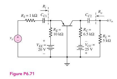
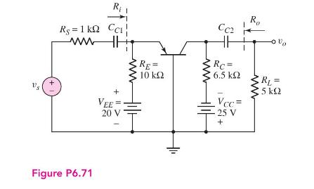
In the common-base circuit shown in Figure P6.71, the transistor is a \(2 \mathrm{~N} 2907 \mathrm{~A}\), with a nominal dc current gain of \(\beta=80\). (a) Determine \(I_{C Q}\) and \(V_{E C Q}\). (b) Using the \(h\)-parameters (assuming \(h_{r e}=0\) ), determine the range in small-signal
In the circuit of Figure P6.71, let \(V_{E E}=V_{C C}=5 \mathrm{~V}, \beta=100, V_{A}=\infty\), \(R_{L}=1 \mathrm{k} \Omega\), and \(R_{S}=0\). (a) Design the circuit such that the small-signal voltage gain is \(A_{v}=v_{o} / v_{s}=25\) and \(V_{E C Q}=3 \mathrm{~V}\). (b) What are the values of
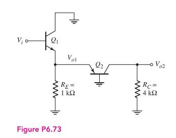
Consider the ac equivalent circuit in Figure P6.73. The transistor parameters are \(\beta_{1}=120, \beta_{2}=80, V_{A 1}=V_{A 2}=\infty\), and \(I_{C Q 1}=I_{C Q 2}=1 \mathrm{~mA}\). (a) Find the small-signal voltage gain \(A_{v 1}=V_{o 1} / V_{i}\). (b) Determine the smallsignal voltage gain
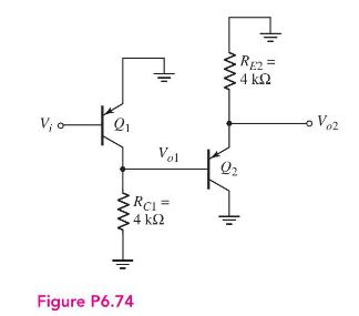
The transistor parameters in the ac equivalent circuit shown in Figure P6.74 are \(\beta_{1}=\beta_{2}=100, V_{A 1}=V_{A 2}=\infty, I_{C Q 1}=0.5 \mathrm{~mA}\), and \(I_{C Q 2}=2 \mathrm{~mA}\).(a) Find the small-signal voltage gain \(A_{v 1}=V_{o 1} / V_{i}\). (b) Determine the small-signal
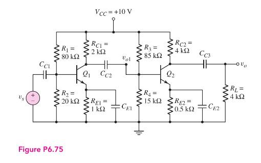
The parameters for each transistor in the circuit shown in Figure P6.75 are \(\beta=100\) and \(V_{A}=\infty\). (a) Determine the small-signal parameters \(g_{m}, r_{\pi}\), and \(r_{o}\) for both transistors. (b) Determine the small-signal voltage gain \(A_{v 1}=v_{o 1} / v_{s}\), assuming \(v_{o
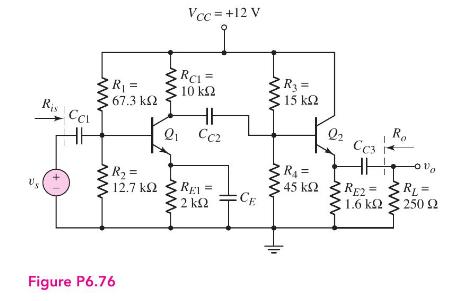
Consider the circuit shown in Figure P6.76 with transistor parameters \(\beta=120\) and \(V_{A}=\infty\). (a) Determine the small-signal parameters \(g_{m}, r_{\pi}\), and \(r_{o}\) for both transistors. (b) Plot the dc and ac load lines for both transistors. (c) Determine the overall small-signal
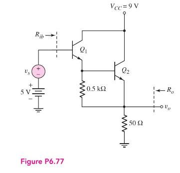
The transistor parameters for the circuit in Figure P6.77 are \(\beta_{1}=120\), \(\beta_{2}=80, V_{B E 1}\) (on) \(=V_{B E 2}\) (on) \(=0.7 \mathrm{~V}\), and \(V_{A 1}=V_{A 2}=\infty\). (a) Determine the quiescent collector current in each transistor. (b) Find the smallsignal voltage gain
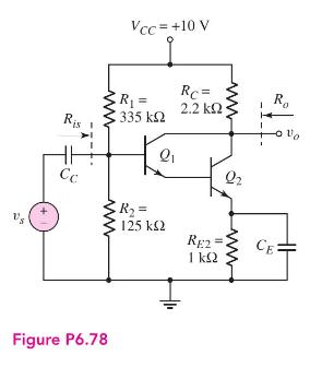
For each transistor in Figure P6.78, the parameters are \(\beta=100\) and \(V_{A}=\infty\). (a) Determine the \(Q\)-point values for both \(Q_{1}\) and \(Q_{2}\). (b) Determine the overall small-signal voltage gain \(A_{v}=v_{o} / v_{s}\). (c) Determine the input and output resistances \(R_{i s}\)
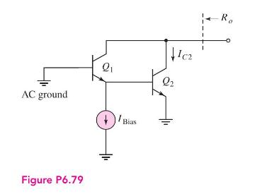
An ac equivalent circuit of a Darlington pair configuration is shown in Figure P6.79. The transistor parameters are \(\beta_{1}=120, \beta_{2}=80, V_{A 1}=80 \mathrm{~V}\), and \(V_{A 2}=50 \mathrm{~V}\). Determine the output resistance \(R_{o}\) for (a) \(I_{C 2}=I_{\text {Bias }}=1
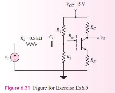
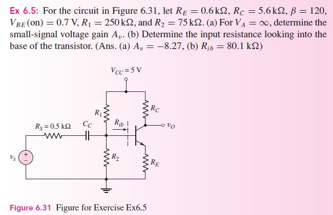
Consider the circuit in Figure 6.31. The circuit and transistor parameters are given in Exercise Ex 6.5.(a) Determine the average power dissipated in the transistor, \(R_{C}\), and \(R_{E}\) for \(v_{s}=0\).(b) Repeat part (a) for \(v_{s}=100 \sin \omega t(\mathrm{mV})\). US Vcc=5 V R Rs = 0.5 k Cc
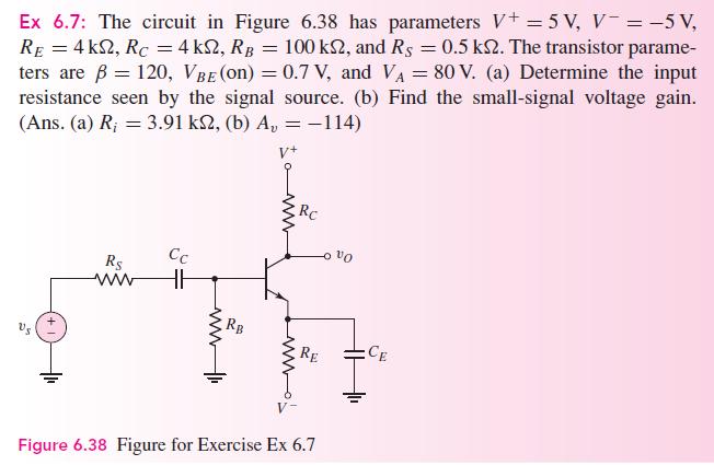
Consider the circuit shown in Figure 6.38. The transistor parameters are given in Exercise Ex 6.7. (a) Calculate the average power dissipated in the transistor, \(R_{C}\), and \(R_{E}\) for \(v_{s}=0\). (b) Determine the maximum undistorted signal power that can be delivered to \(R_{C}\) for the
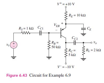
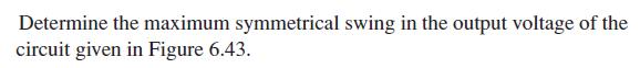
For the circuit shown in Figure 6.43, use the circuit and transistor parameters described in Example 6.9. (a) Calculate the average power dissipated in the transistor, \(R_{E}\), and \(R_{C}\), for \(v_{s}=0\). (b) Determine the maximum signal power that can be delivered to \(R_{L}\). What are the
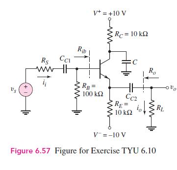
For the circuit shown in Figure 6.57, the transistor parameters are \(\beta=100\) and \(V_{A}=100 \mathrm{~V}\), and the source resistor is \(R_{S}=0\). Determine the maximum undistorted signal power that can be delivered to \(R_{L}\) if: (a) \(R_{L}=\) \(1 \mathrm{k} \Omega\), and (b) \(R_{L}=10
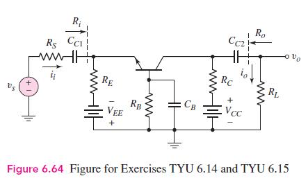
Consider the circuit shown in Figure 6.64 with parameters given in Exercise TYU 6.14. (a) Calculate the average power dissipated in the transistor and \(R_{C}\), for \(v_{s}=0\). (b) Determine the maximum undistorted signal power that can be delivered to \(R_{L}\), and the resulting average power
(a) Using a computer simulation, verify the results of Exercise Ex 6.5.(b) Repeat part (a) for Early voltages of (i) \(V_{A}=100 \mathrm{~V}\) and (ii) \(V_{A}=50 \mathrm{~V}\).Data From Exercise Ex 6.5:- Ex 6.5: For the circuit in Figure 6.31, let RE = 0.6k, Rc = 5.6k, p = 120, VBE (on) = 0.7 V, R
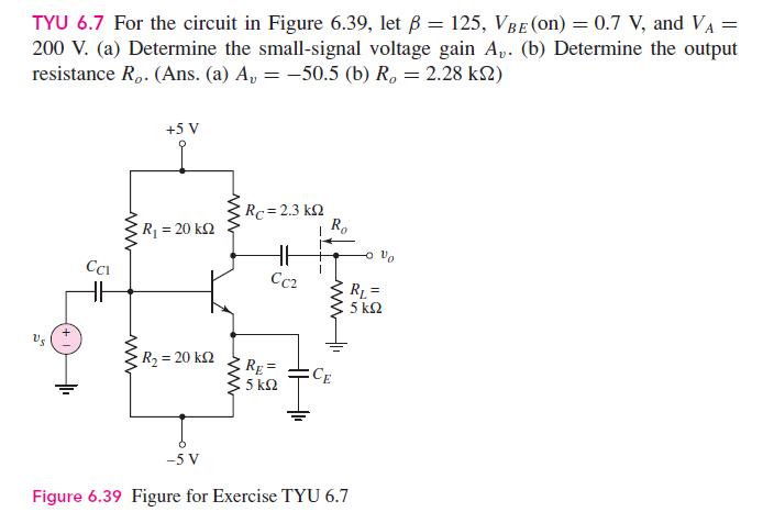
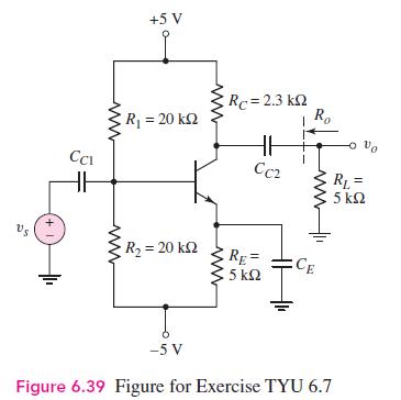
(a) Using a computer simulation, verify the results of Exercise TYU 6.7.s(b) Repeat part (a) for an Early voltage of \(V_{A}=50 \mathrm{~V}\).Data From Exercise TYU 6.7:- = TYU 6.7 For the circuit in Figure 6.39, let = 125, VBE (on) = 0.7 V, and VA 200 V. (a) Determine the small-signal voltage
Using a computer simulation, verify the results of Example 6.10.Data From Example 6.10:- Determine the maximum symmetrical swing in the output voltage of the circuit given in Figure 6.43.
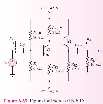
Using a computer simulation, verify the results of Exercise Ex 6.15 for the multi transistor amplifier.Data From Exercise Ex 6.15:- Ex 6.15: For each transistor in the circuit in Figure 6.69, the parameters are: B = 125, VBE (on) = 0.7 V, and r = . (a) Determine the Q-points of each tran- sistor.
Design a common-emitter amplifier with the general configuration shown in Figure 6.39 except with a pnp transistor. The magnitude of the small-signal voltage gain should be \(\left|A_{v}\right|=50\) while driving a load \(R_{L}=10 \mathrm{k} \Omega\). Bias the circuit at \(\pm 3.3\mathrm{~V}\). +-
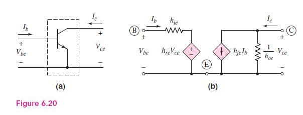
Consider the circuit in Figure 6.20. Let \(V_{C C}=5 \mathrm{~V}, R_{L}=10 \mathrm{k} \Omega, \beta=120\), and \(V_{A}=\infty\). Design the circuit such that the small-signal current gain is \(A_{i}=20\) and such that the maximum undistorted swing in the output voltage is achieved. + V be Figure
A microphone puts out a peak voltage of \(2 \mathrm{mV}\) and has an output resistance of \(5 \mathrm{k} \Omega\). Design an amplifier system to drive a \(24 \Omega\) speaker, producing \(0.5 \mathrm{~W}\) of signal power. Assume a current gain of \(\beta=50\) for all available transistors. Specify
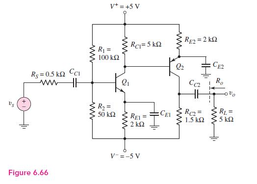
Redesign the two-stage amplifier in Figure 6.66 such that the voltage gain of each stage is \(A_{v 1}=A_{v 2}=-50\). Assume transistor current gains of \(\beta_{\text {npn }}=150\) and \(\beta_{\text {pnp }}=110\). The total power dissipated in the circuit should be limited to \(25 \mathrm{~mW}\).
Describe the general frequency response of an amplifier and define the low frequency, midband, and high-frequency ranges.
Describe the general characteristics of the equivalent circuits that apply to the low-frequency, midband, and high-frequency ranges.
Describe what is meant by a system transfer function in the \(s\)-domain.
What is the criterion that defines a corner, or \(3 \mathrm{~dB}\), frequency?
Describe what is meant by the phase of the transfer function.
Describe the time constant technique for determining the corner frequencies.
Describe the general frequency response of a coupling capacitor, a bypass capacitor, and a load capacitor.
Sketch the expanded hybrid- \(\pi\) model of the BJT.
Describe the short-circuit current gain versus frequency response of a BJT and define the cutoff frequency.
Describe the Miller effect and the Miller capacitance.
What effect does the Miller capacitance have on the amplifier bandwidth?
Sketch the expanded small-signal equivalent circuit of a MOSFET.
Define the cutoff frequency for a MOSFET.
What is the major contribution to the Miller capacitance in a MOSFET?
Why is there not a Miller effect in a common-base circuit?
Describe the configuration of a cascode amplifier.
Why is the bandwidth of a cascode amplifier larger, in general, than that of a simple common-emitter amplifier?
Why is the bandwidth of the emitter-follower amplifier the largest of the three basic BJT amplifiers?
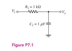
(a) Determine the voltage transfer function \(T(s)=V_{o}(s) / V_{i}(s)\) for the circuit shown in Figure P7.1. (b) Sketch the Bode magnitude plot and determine the corner frequency. (c) Determine the time response of the circuit to an input step function of magnitude \(V_{I o}\). Vio R = 1 kQ ww C
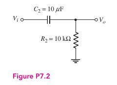
Repeat Problem 7.1 for the circuit in Figure P7.2.Data From Problem 7.1:-(a) Determine the voltage transfer function \(T(s)=V_{o}(s) / V_{i}(s)\) for the circuit shown in Figure P7.1. (b) Sketch the Bode magnitude plot and determine the corner frequency. (c) Determine the time response of the
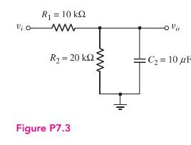
Consider the circuit in Figure P7.3. (a) Derive the expression for the voltage transfer function \(T(s)=V_{o}(s) / V_{i}(s)\). (b) What is the time constant associated with this circuit? (c) Find the corner frequency. (d) Sketch the Bode magnitude plot of the voltage transfer function. R1 = 10 www
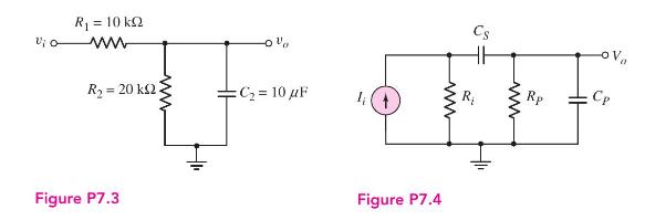
Consider the circuit in Figure P7.4 with a signal current source. The circuit parameters are \(R_{i}=30 \mathrm{k} \Omega, R_{P}=10 \mathrm{k} \Omega, C_{S}=10 \mu \mathrm{F}\), and \(C_{P}=50 \mathrm{pF}\).(a) Determine the open-circuit time constant associated with \(C_{S}\) and the short-circuit
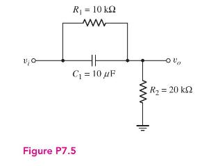
Consider the circuit shown in Figure P7.5. (a) What is the value of the voltage transfer function \(V_{o} / V_{i}\) at very low frequencies? (b) Determine the voltage transfer function at very high frequencies. (c) Derive the expression for the voltage transfer function \(T(s)=V_{o}(s) /
(a) Derive the voltage transfer function \(T(s)=V_{o}(s) / V_{i}(s)\) for the circuit shown in Figure 7.10, taking both capacitors into account.(b) Let \(R_{S}=R_{P}=10 \mathrm{k} \Omega, C_{S}=1 \mu \mathrm{F}\), and \(C_{P}=10 \mathrm{pF}\). Calculate the actual magnitude of the transfer function
A voltage transfer function is given by \(T(f)=1 /\left(1+j f / f_{T}\right)^{3}\). (a) Show that the actual response at \(f=f_{T}\) is approximately \(9 \mathrm{~dB}\) below the maximum value. What is the phase angle at this frequency? (b) What is the slope of the magnitude plot for \(f \gg
Sketch the Bode magnitude plots for the following functions:(a) \(T_{1}(s)=\frac{s}{s+100}\)(b) \(T_{2}(s)=\frac{5}{s / 2000+1}\)(c) \(T_{3}(s)=\frac{200(s+10)}{(s+1000)}\)
(a) (i) Sketch the Bode magnitude plot for the function\[T(s)=\frac{10(s+10)(s+100)}{(s+1)(s+1000)}\](ii) What are the corner frequencies?(iii) Determine \(|T(\omega)|\) for \(\omega \rightarrow 0\).(iv) Determine \(|T(\omega)|\) for \(\omega \rightarrow \infty\).(b) Repeat part (a) for the
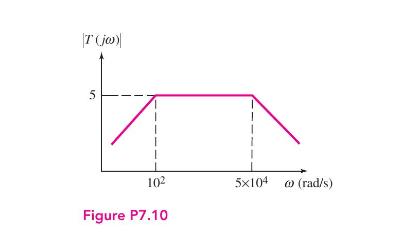
(a) Determine the transfer function corresponding to the Bode plot of the magnitude shown in Figure P7.10. (b) What is the actual gain at (i) \(\omega=50 \mathrm{rad} / \mathrm{s}\), (ii) \(\omega=150 \mathrm{rad} / \mathrm{s}\), and (iii) \(\omega=100 \mathrm{krad} / \mathrm{s}\). T(jw) 5 102
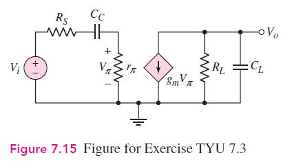
Consider the circuit shown in Figure 7.15 with parameters \(R_{S}=0.5 \mathrm{k} \Omega\), \(r_{\pi}=5.2 \mathrm{k} \Omega, g_{m}=29 \mathrm{~mA} / \mathrm{V}\), and \(R_{L}=6 \mathrm{k} \Omega\). The corner frequencies are \(f_{L}=30 \mathrm{~Hz}\) and \(f_{H}=480 \mathrm{kHz}\). (a) Calculate the
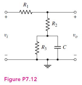
For the circuit shown in Figure P7.12, the parameters are \(R_{1}=10 \mathrm{k} \Omega\), \(R_{2}=10 \mathrm{k} \Omega, R_{3}=40 \mathrm{k} \Omega\), and \(C=10 \mu \mathrm{F}\). (a) What is the value of the voltage transfer function \(V_{o} / V_{i}\) at very low frequencies? (b) Determine the
The circuit shown in Figure 7.10 has parameters \(R_{S}=1 \mathrm{k} \Omega, R_{P}=10 \mathrm{k} \Omega\), and \(C_{S}=C_{P}=0.01 \mu \mathrm{F}\). Using PSpice, plot the magnitude and phase of the voltage transfer function. Determine the maximum value of the voltage transfer function. Determine
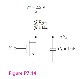
The transistor shown in Figure P7.14 has parameters \(V_{T N}=0.4 \mathrm{~V}\), \(K_{n}=0.4 \mathrm{~mA} / \mathrm{V}^{2}\), and \(\lambda=0\). The transistor is biased at \(I_{D Q}=0.8 \mathrm{~mA}\). (a) What is the maximum voltage gain? (b) What is the bandwidth? V o V+ = 2.5 V Figure P7.14 RD=
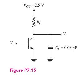
Consider the circuit shown in Figure P7.15. The transistor has parameters \(\beta=120\) and \(V_{A}=\infty\). The circuit bandwidth is \(800 \mathrm{MHz}\) and the quiescent collector-emitter voltage is \(V_{C E Q}=1.25 \mathrm{~V}\). (a) Determine \(R_{C}\), (b) find \(I_{C Q}\), and (c) determine
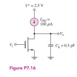
The transistor in the circuit shown in Figure P7.16 has parameters \(V_{T N}=0.4 \mathrm{~V}, K_{n}=50 \mu \mathrm{A} / \mathrm{V}^{2}\), and \(\lambda=0.01 \mathrm{~V}^{-1}\). (a) Derive the expression for the voltage transfer function \(T(s)=V_{o}(s) / V_{i}(s)\). (b) Determine the maximum
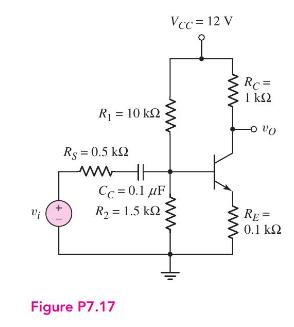
For the common-emitter circuit in Figure P7.17, the transistor parameters are: \(\beta=100, V_{B E}(\) on \()=0.7 \mathrm{~V}\), and \(V_{A}=\infty\). (a) Calculate the lower corner frequency. (b) Determine the midband voltage gain. (c) Sketch the Bode plot of the voltage gain magnitude. Vi = Vcc
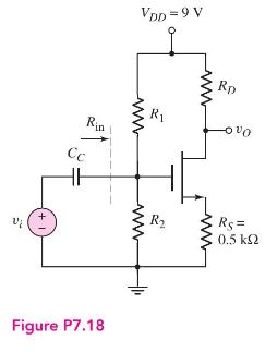
(a) Design the circuit shown in Figure P7.18 such that \(I_{D Q}=0.8 \mathrm{~mA}\), \(V_{D S Q}=3.2 \mathrm{~V}, R_{\text {in }}=160 \mathrm{k} \Omega\), and \(f_{L}=16 \mathrm{~Hz}\). The transistor parameters are \(K_{n}=0.5 \mathrm{~mA} / \mathrm{V}^{2}, V_{T N}=1.2 \mathrm{~V}\), and
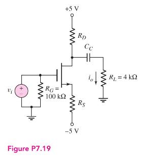
The transistor in the circuit in Figure P7.19 has parameters \(K_{n}=\) \(0.5 \mathrm{~mA} / \mathrm{V}^{2}, V_{T N}=1 \mathrm{~V}\), and \(\lambda=0\).(a) Design the circuit such that \(I_{D Q}=\) \(1 \mathrm{~mA}\) and \(V_{D S Q}=3 \mathrm{~V}\).(b) Derive the expression for the transfer
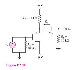
The transistor in the circuit in Figure P7.20 has parameters \(K_{p}=\) \(0.5 \mathrm{~mA} / \mathrm{V}^{2}, V_{T P}=-2 \mathrm{~V}\), and \(\lambda=0\). (a) Determine \(R_{o}\). (b) What is the expression for the circuit time constant? (c) Determine \(C_{C}\) such that the lower \(3 \mathrm{~dB}\)
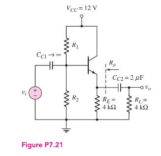
For the circuit in Figure P7.21, the transistor parameters are \(\beta=120\), \(V_{B E}(\) on \()=0.7 \mathrm{~V}\), and \(V_{A}=50 \mathrm{~V}\). (a) Design a bias-stable circuit such that \(I_{E Q}=1.5 \mathrm{~mA}\). (b) Using the results of part (a), find the small-signal midband voltage gain.
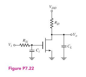
(a) For the circuit shown in Figure P7.22, write the voltage transfer function \(T(s)=V_{o}(s) / V_{i}(s)\). Assume \(\lambda>0\) for the transistor. (b) What is the expression for the time constant associated with the input portion of the circuit? (c) What is the expression for the time
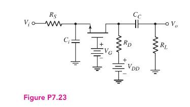
Consider the circuit shown in Figure P7.23. (a) Write the transfer function \(T(s)=V_{o}(s) / V_{i}(s)\). Assume \(\lambda=0\) for the transistor. (b) Determine the expression for the time constant associated with the input portion of the circuit. (c) Determine the expression for the time constant
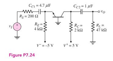
The parameters of the transistor in the circuit in Figure P7.24 are \(V_{B E}(\) on \()=0.7 \mathrm{~V}, \beta=100\), and \(V_{A}=\infty\). (a) Determine the quiescent and small-signal parameters of the transistor. (b) Find the time constants associated with \(C_{C 1}\) and \(C_{C 2}\). (c) Is
A capacitor is placed in parallel with \(R_{L}\) in the circuit in Figure P7.24. The capacitance is \(C_{L}=10 \mathrm{pF}\). The transistor parameters are the same as given in Problem 7.24. (a) Determine the upper \(-3 \mathrm{~dB}\) frequency. (b) Find the high frequency value at which the
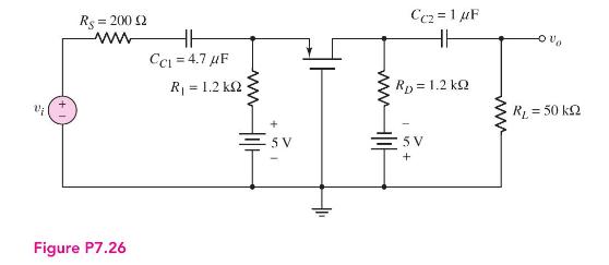
The parameters of the transistor in the circuit in Figure P7.26 are \(K_{p}=\) \(1 \mathrm{~mA} / \mathrm{V}^{2}, V_{T P}=-1.5 \mathrm{~V}\), and \(\lambda=0\). (a) Determine the quiescent and small-signal parameters of the transistor. (b) Find the time constants associated with \(C_{C 1}\) and
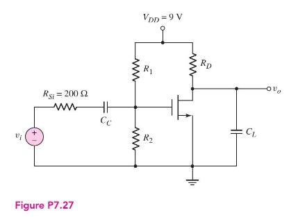
A MOSFET amplifier with the configuration in Figure P7.27 is to be designed for use in a telephone circuit. The magnitude of the voltage gain should be 10 in the midband range, and the midband frequency range should extend from \(200 \mathrm{~Hz}\) to \(3 \mathrm{kHz}\). [Note: A telephone's
The circuit in Figure P7.28 is a simple output stage of an audio amplifier. The transistor parameters are \(\beta=200, V_{B E}(\) on \()=0.7 \mathrm{~V}\), and \(V_{A}=\infty\). Determine \(C_{C}\) such that the lower \(-3 \mathrm{~dB}\) frequency is \(15 \mathrm{~Hz}\).
Reconsider the circuit in Figure P7.28. The transistor parameters are \(\beta=120, V_{B E}\) (on) \(=0.7 \mathrm{~V}\), and \(V_{A}=\infty\). The circuit parameters are \(V^{+}=\) \(3.3 \mathrm{~V}\) and \(R_{S}=100 \Omega\). (a) Find \(R_{B}\) and \(R_{E}\) such that \(I_{E Q}=0.25 \mathrm{~mA}\)
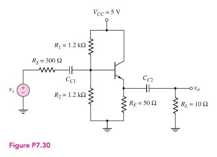
The parameters of the transistor in the circuit in Figure P7.30 are \(\beta=100\), \(V_{B E}\) (on) \(=0.7 \mathrm{~V}\), and \(V_{A}=\infty\). The time constant associated with \(C_{C 1}\) is a factor of 100 larger than the time constant associated with \(C_{C 2}\). (a) Determine \(C_{C 2}\) such
Consider the circuit shown in Figure P7.30. The time constant associated with \(C_{C 2}\) is a factor of 100 larger than the time constant associated with \(C_{C 1}\). (a) Determine \(C_{C 1}\) such that the \(-3 \mathrm{~dB}\) frequency associated with this capacitor is \(20 \mathrm{~Hz}\). (b)
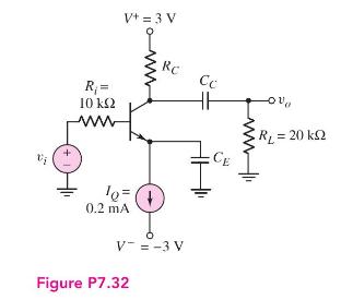
Consider the circuit shown in Figure P7.32. The transistor parameters are \(\beta=120, V_{B E}\) (on) \(=0.7 \mathrm{~V}\), and \(V_{A}=\infty\). (a) Find \(R_{C}\) such that \(V_{C E Q}=2.2 \mathrm{~V}\). (b) Determine the midband gain. (c) Derive the expression for the corner frequencies
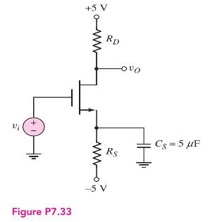
For the transistor in the circuit in Figure P7.33, the parameters are: \(K_{n}=0.5 \mathrm{~mA} / \mathrm{V}^{2}, V_{T N}=0.8 \mathrm{~V}\), and \(\lambda=0\). (a) Design the circuit such that \(I_{D Q}=0.5 \mathrm{~mA}\) and \(V_{D S Q}=4 \mathrm{~V}\). (b) Determine the \(3 \mathrm{~dB}\)
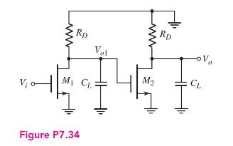
Figure P7.34 shows the ac equivalent circuit of two identical commonsource circuits in cascade. The transistor parameters are \(K_{n 1}=K_{n 2}=\) \(0.8 \mathrm{~mA} / \mathrm{V}^{2}, \lambda_{1}=\lambda_{2}=0.02 \mathrm{~V}^{-1}\), and \(I_{D Q 1}=I_{D Q 2}=0.5 \mathrm{~mA}\). The circuit
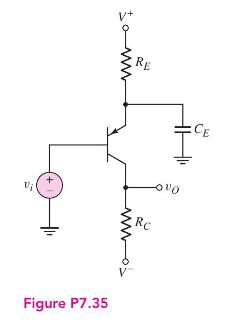
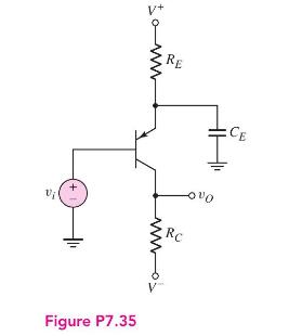
The common-emitter circuit in Figure P7.35 has an emitter bypass capacitor. (a) Derive the expression for the small-signal voltage gain \(A_{v}(s)=V_{o}(s) / V_{i}(s)\). Write the expression in a form similar to that of Equation (7.60). (b) What are the expressions for the time constants
Consider the circuit in Figure P7.35. The bias voltages are \(V^{+}=3 \mathrm{~V}\) and \(V^{-}=-3 \mathrm{~V}\). The transistor parameters are \(\beta=90, V_{E B}(\mathrm{on})=0.7 \mathrm{~V}\) and \(V_{A}=\infty\). (a) Design the circuit such that \(I_{C Q}=0.15 \mathrm{~mA}\) and \(V_{E C Q}=2.2
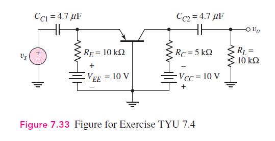
Consider the common-base circuit in Figure 7.33 in the text. The transistor parameters are \(\beta=90, V_{E B}(\mathrm{on})=0.7 \mathrm{~V}\), and \(V_{A}=\infty\). A load capacitance of \(C_{L}=3 \mathrm{pF}\) is connected in parallel with \(R_{L}\). (a) Determine the midband voltage gain. (b)
Consider the circuit shown in Figure 7.25(a). The bias voltages are changed to \(V^{+}=3 \mathrm{~V}\) and \(V^{-}=-3 \mathrm{~V}\). The load resistor is \(R_{L}=20 \mathrm{k} \Omega\). The transistor parameters are \(K_{p}=0.1 \mathrm{~mA} / \mathrm{V}^{2}, V_{T P}=-0.6 \mathrm{~V}\), and
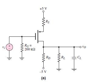
For the circuit in Figure P7.39, the transistor parameters are: \(K_{n}=\) \(0.5 \mathrm{~mA} / \mathrm{V}^{2}, V_{T N}=2 \mathrm{~V}\), and \(\lambda=0\). Determine the maximum value of \(C_{L}\) such that the bandwidth is at least \(B W=5 \mathrm{MHz}\). State any approximations or assumptions
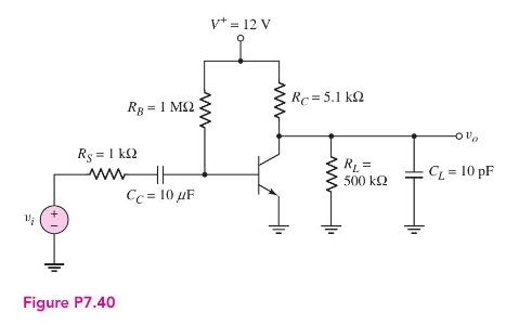
The parameters of the transistor in the circuit in Figure P7.40 are \(\beta=100\), \(V_{B E}\) (on) \(=0.7 \mathrm{~V}\), and \(V_{A}=\infty\). Neglect the capacitance effects of the transistor. (a) Draw the three equivalent circuits that represent the amplifier in the low-frequency range, midband
In the common-source amplifier in Figure 7.25(a) in the text, a source bypass capacitor is to be added between the source terminal and ground potential. The circuit parameters are \(R_{S}=3.2 \mathrm{k} \Omega, R_{D}=10 \mathrm{k} \Omega, R_{L}=20 \mathrm{k} \Omega\), and \(C_{L}=10 \mathrm{pF}\).
Consider the common-base circuit in Figure P7.42. Choose appropriate transistor parameters. (a) Using a computer analysis, generate the Bode plot of the voltage gain magnitude from a very low frequency to the midband frequency range. At what frequency is the voltage gain magnitude \(3
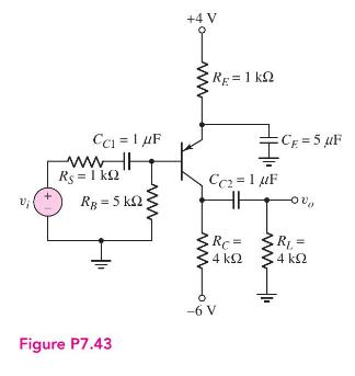
For the common-emitter circuit in Figure P7.43, choose appropriate transistor parameters and perform a computer analysis. Generate the Bode plot of the voltage gain magnitude from a very low frequency to the midband frequency range. At what frequency is the voltage gain magnitude \(3 \mathrm{~dB}\)
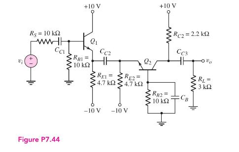
For the multitransistor amplifier in Figure P7.44, choose appropriate transistor parameters. The lower \(3 \mathrm{~dB}\) frequency is to be less than or equal to \(20 \mathrm{~Hz}\). Assume that all three coupling capacitors are equal. Let \(C_{B} \rightarrow \infty\). Using a computer analysis,
A bipolar transistor has \(f_{T}=4 \mathrm{GHz}, \beta_{o}=120\), and \(C_{\mu}=0.08 \mathrm{pF}\) when operated at \(I_{C Q}=0.25 \mathrm{~mA}\). Determine \(g_{m}, f_{\beta}\), and \(C_{\pi}\).
A high-frequency bipolar transistor is biased at \(I_{C Q}=0.4 \mathrm{~mA}\) and has parameters \(C_{\mu}=0.075 \mathrm{pF}, f_{T}=2 \mathrm{GHz}\), and \(\beta_{o}=120\). (a) Determine \(C_{\pi}\) and \(f_{\beta}\). (b) Determine \(\left|h_{f e}\right|\) at (i) \(f=10 \mathrm{MHz}\), (ii) \(f=20
(a) The frequency \(f_{T}\) of a bipolar transistor is found to be \(540 \mathrm{MHz}\) when biased at \(I_{C Q}=0.2 \mathrm{~mA}\). The transistor parameters are \(C_{\mu}=0.4 \mathrm{pF}\) and \(\beta_{o}=120\). Determine \(f_{\beta}\) and \(C_{\pi}\). (b) Using the results of part (a), determine
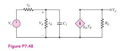
The circuit in Figure P7.48 is a hybrid- \(\pi\) equivalent circuit including the resistance \(r_{b}\). (a) Derive the expression for the voltage gain transfer function \(A_{v}(s)=V_{o}(s) / V_{i}(s)\). (b) If the transistor is biased at \(I_{C Q}=1 \mathrm{~mA}\), and if \(R_{L}=4 \mathrm{k}
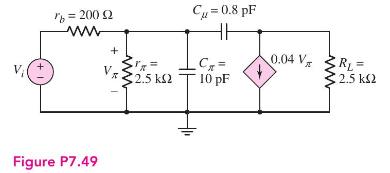
Consider the circuit in Figure P7.49. Calculate the impedance seen by the signal source \(V_{i}\) at (a) \(f=1 \mathrm{kHz}\), (b) \(f=10 \mathrm{kHz}\), (c) \(f=100 \mathrm{kHz}\), and (d) \(f=1 \mathrm{MHz}\). 1+ b = 200 2 ww + Figure P7.49 C = 0.8 pF V. 32.5 10 pF 0.04 V, RL= 2.5 ks2
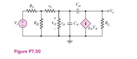
A common-emitter equivalent circuit is shown in Figure P7.50. (a) What is the expression for the Miller capacitance? (b) Derive the expression for the voltage gain \(A_{v}(s)=V_{o}(s) / V_{i}(s)\) in terms of the Miller capacitance and other circuit parameters. (c) What is the expression for the
For the common-emitter circuit in Figure 7.41 (a) in the text, assume that \(r_{s}=\infty, R_{1} \| R_{2}=5 \mathrm{k} \Omega\), and \(R_{C}=R_{L}=1 \mathrm{k} \Omega\). The transistor is biased at \(I_{C Q}=5 \mathrm{~mA}\) and the parameters are: \(\beta_{o}=200, V_{A}=\infty, C_{\mu}=5
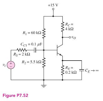
For the common-emitter circuit in Figure P7.52, assume the emitter bypass capacitor \(C_{E}\) is very large, and the transistor parameters are: \(\beta_{o}=100\), \(V_{B E}(\) on \()=0.7 \mathrm{~V}, V_{A}=\infty, C_{\mu}=2 \mathrm{pF}\), and \(f_{T}=400 \mathrm{MHz}\). Determine the lower and
Consider the circuit in Figure P7.52. The resistor \(R_{S}\) is changed to \(500 \Omega\) and all other resistor values are increased by a factor of 10 . The transistor parameters are the same as listed in Problem 7.52. Determine the lower and upper \(-3 \mathrm{~dB}\) frequencies for the voltage
The parameters of the circuit shown in Figure P7.52 are changed to \(V^{+}=5 \mathrm{~V}, R_{S}=0, R_{1}=33 \mathrm{k} \Omega, R_{2}=22 \mathrm{k} \Omega, R_{C}=5 \mathrm{k} \Omega\), and \(R_{E}=4 \mathrm{k} \Omega\). The transistor parameters are \(\beta_{o}=150, C_{\mu}=0.45 \mathrm{pF}\), and
The parameters of an n-channel MOSFET are \(k_{n}^{\prime}=80 \mu \mathrm{A} / \mathrm{V}^{2}, W=4 \mu \mathrm{m}\), \(L=0.8 \mu \mathrm{m}, C_{g s}=50 \mathrm{fF}\), and \(C_{g d}=10 \mathrm{fF}\). The transistor is biased at \(I_{D Q}=0.6 \mathrm{~mA}\). Determine \(f_{T}\).
Find \(f_{T}\) for a MOSFET biased at \(I_{D Q}=120 \mu \mathrm{A}\) and \(V_{G S}-V_{T N}=0.20 \mathrm{~V}\). The transistor parameters are \(C_{g s}=40 \mathrm{fF}\) and \(C_{g d}=10 \mathrm{fF}\).
Showing 1100 - 1200
of 4723
First
5
6
7
8
9
10
11
12
13
14
15
16
17
18
19
Last
Step by Step Answers