New Semester
Started
Get
50% OFF
Study Help!
--h --m --s
Claim Now
Question Answers
Textbooks
Find textbooks, questions and answers
Oops, something went wrong!
Change your search query and then try again
S
Books
FREE
Study Help
Expert Questions
Accounting
General Management
Mathematics
Finance
Organizational Behaviour
Law
Physics
Operating System
Management Leadership
Sociology
Programming
Marketing
Database
Computer Network
Economics
Textbooks Solutions
Accounting
Managerial Accounting
Management Leadership
Cost Accounting
Statistics
Business Law
Corporate Finance
Finance
Economics
Auditing
Tutors
Online Tutors
Find a Tutor
Hire a Tutor
Become a Tutor
AI Tutor
AI Study Planner
NEW
Sell Books
Search
Search
Sign In
Register
study help
computer science
systems analysis design
The Analysis And Design Of Linear Circuits 10th Edition Roland E. Thomas, Albert J. Rosa, Gregory J. Toussaint - Solutions
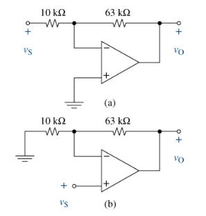
Find the voltage gain of each OP AMP circuit shown in Figure P4-19. Vs 10 10 + VS 63 + (2) 63 + (b) VO +
Considering simplicity and standard 10\% tolerance resistors from Appendix G as major constraints, design circuits with a single OP AMP that produce the following voltage gains \(\pm 10 \%:-50,+201,-0.91,-1000,+0.8,-1,+1\).
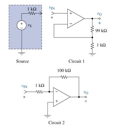
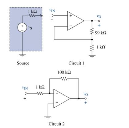
Two OP AMP circuits are shown in Figure P4-21. Both claim to produce a gain of either \(\pm 100\).(a) Show that the claim is true.(b) A practical source with a series resistor of \(1 \mathrm{k} \Omega\) is connected to the input of each circuit. Does the original claim still hold? If it does not,
Suppose the output of the practical source shown in Figure P4-21 needs to be amplified by \(-10^{4}\) and you can use only the two circuits shown. How would you connect the circuits to achieve this? Explain why. VIN Source + VS 1 1 VIN + Circuit 1 100 Circuit 2 VO VO + 99 1
(a) Find the voltage gain \(v_{\mathrm{O}} / v_{\mathrm{S}}\) in Figure \(\mathrm{P}_{4}=23\). What is the range of the input that can be amplified without causing the OP AMP to saturate?(b) Validate your answers by simulating the circuit in Multisim. Sweep the voltage source from \(-5
(a) Using only one OP AMP, design a simple circuit that has a variable gain from -10 to -500 .(b) Using only one OP AMP, design a simple circuit that has a variable gain from +10 to +500 .
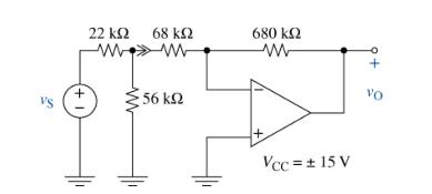
Using only one OP AMP per circuit with a \(V_{\mathrm{CC}}\) of \(\pm 15 \mathrm{~V}\), design circuits that realize the following equations:\[\begin{aligned}& v_{\mathrm{O}}=5 v_{1}-3.3 \mathrm{~V} \\& v_{\mathrm{O}}=5 v_{1}+3.3 \mathrm{~V}\end{aligned}\]
Two non-OP AMP circuits need to be connected in cascade. Explain why using a follower is more useful than simply connecting the two circuits using wires. Are there any downsides to using a follower?
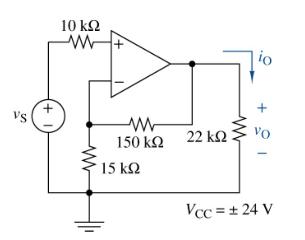
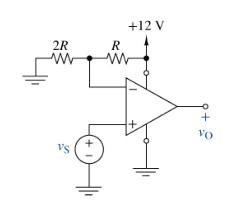
For the circuit in Figure P4-27:(a) Find \(v_{\mathrm{O}}\) in terms of \(v_{\mathrm{S}}\).(b) Find \(i_{\mathrm{O}}\) for \(v_{\mathrm{S}}=1 \mathrm{~V}\). Repeat for \(v_{\mathrm{S}}=3 \mathrm{~V}\). VS + 10 150 22 15 io VO Vcc = 24 V
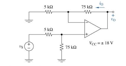
For the circuit in Figure P4-28 :(a) Find \(v_{\mathrm{O}}\) in terms \(v_{\mathrm{S}}\).(b) Find \(i_{\mathrm{O}}\) and \(v_{\mathrm{O}}\) for \(v_{\mathrm{S}}=1 \mathrm{~V}\). Repeat for \(v_{\mathrm{S}}=2 \mathrm{~V}\).(c) Validate your answers using Multisim.(d) What could you do to avoid
Design two circuits to produce the following out-put: \(v_{\mathrm{O}}=2 v_{1}-4 v_{2}\).(a) In your first design, use a standard subtractor.(b) In your second design, both inputs must be into high input resistance amplifiers to avoid loading.
Design a noninverting summer for five inputs with equal gains of 5 .
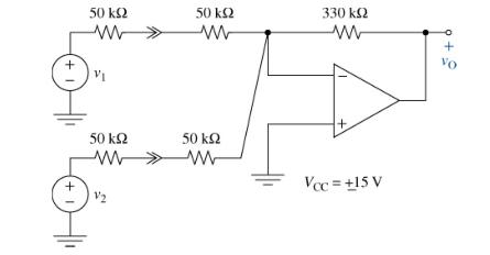
For the circuit in Figure P4=31 :(a) Find \(v_{\mathrm{O}}\) in terms of the inputs \(v_{1}\) and \(v_{2}\).(b) If \(v_{1}=1 \mathrm{~V}\), what is the range of values \(v_{2}\) can have without saturating the OP AMP? + + 50 VI 50 12 50 50 330 V@c = +15V + VO
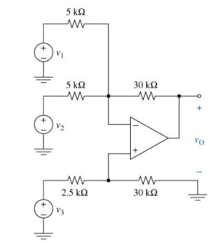
Find \(v_{\mathrm{O}}\) in terms of the inputs \(v_{1}, v_{2}\), and \(v_{3}\) in Figure \(\underline{P}_{4}=3 \underline{2}\). + V 1 5 V3 5 2.5 30 30 VO
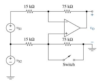
The switch in Figure \(\mathrm{P}_{4}=33\) is open. Find \(v_{\mathrm{O}}\) in terms of the inputs \(v_{\mathrm{S} 1}\) and \(v_{\mathrm{S} 2}\). Repeat with the switch closed. (+1 +1 | VS1 | VS2 15 15 75 75 Switch + VO
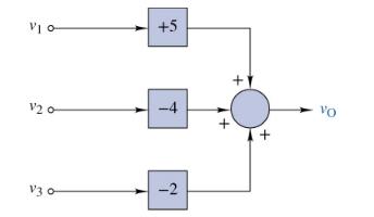
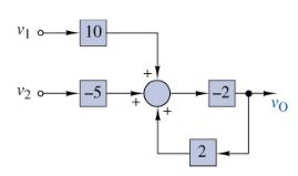
(a) Design an OP AMP circuit that realizes the block diagram shown in Figure P4=34. Do not use more than two OP AMPs in your design.(b) Can you do the design with only one OP AMP?(c) Simulate your results using Multisim. Assume all sources are \(1 \mathrm{~V}\). VI 0- 12 0 V30- +5 -4 -2 + VO
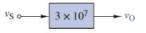
Design an OP AMP circuit that realizes the block diagram shown in Figure P4=35 . The OP AMPs that you must use have a maximum gain of 3000 . VS o 3 x 10⁷ -Vo
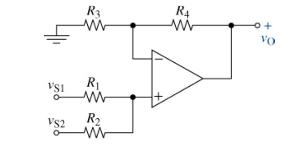
For the circuit in Figure P4=3(a) Find \(v_{\mathrm{O}}\) in terms of \(v_{\mathrm{S} 1}\) and \(v_{\mathrm{S} 2}\).(b) Select values so that \(v_{\mathrm{O}}=v_{\mathrm{S} 1}+9 v_{\mathrm{S} 2}\). VSI VS2 R R ww R ww R W 0+ VO
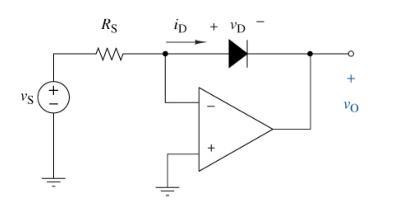
The circuit in Figure P4=37 has a diode in its feedback path and is called a "log-amp" because its output is proportional to the natural \(\log\) of the input.(a) Show that \({ }^{v_{\mathrm{O}}=-V_{\mathrm{T}} \ln \left(1+\frac{v_{\mathrm{S}}}{R_{\mathrm{S}} \mathrm{S}_{\mathrm{O}}}ight)}\) if the
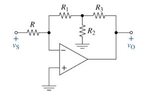
(a) Use node-voltage analysis to find the input-output relationship or \(K\) of the circuit in Figure P4 \(4 \underline{3}\).(b) Select values for the resistors so that \(K=-100\). + VS R R ww R3 ww {R o+ VO
For the circuit of Figure P4=3.9:(a) With \(v_{2}=2 \mathrm{~V}\), find the output in terms of \(v_{1}\). Is there a value of \(v_{1}\) that would cause the output to saturate?(b) Draw a block diagram for the circuit.(c) With \(v_{1}=2 \mathrm{~V}\), find the output in terms of \(v_{2}\). Is there
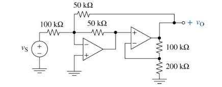
For the circuit of Figure P4-4으 :(a) Find the output in terms of \(v_{\mathrm{S}}\).(b) Draw a block diagram for the circuit. VS 100 50 50 o + Vo 100 200
For the block diagram of Figure P4-41 :(a) Find an expression for \(v_{\mathrm{O}}\) in terms of \(v_{1}\) and \(v_{2}\).(b) Design a suitable circuit that realizes the block diagram using only one OP AMP. VI V20 10 2 VO
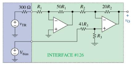
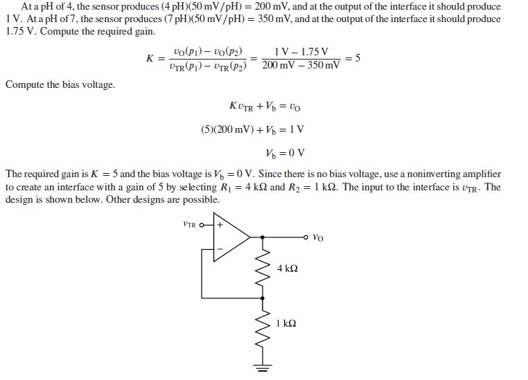
(D) A certain transducer, shown in Figure P4-42, needs a circuit that realizes the following interface \(v_{\mathrm{O}}=1000 v\) TR \(+0.75 \mathrm{~V}\). A search in a vendor's catalog showed that their INTERFACE \#126, with properly defined resistors and a suitable bias voltage, could work.(a) 1
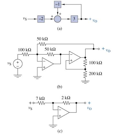
On a quiz, an instructor asked the students to draw a circuit that would realize the block diagram shown in Figure P4-43(a). One student drew the circuit shown in Figure P4-43(b). Another student drew the circuit in Figure P4–43(c). Determine the correct solution and grade the two students. VS VS
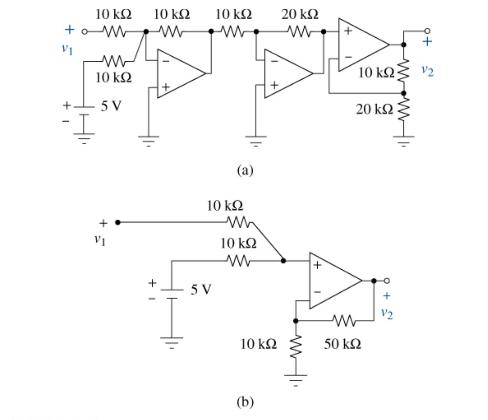
On an exam, students were asked to design an efficient solution for the following relationship: \(v_{2}=3 v_{1}+15\). Two of the designs are shown in Figure P4-44. Which, if any, of the designs are correct and what grade would you award each student? 10 to w 10 SV 10 5V 10 (2) 10 10 10
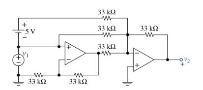
For the circuit of Figure P4-45:(a) Simplify the circuit to using only one OP AMP.(b) Draw a representative block diagram for the circuit. +1 5V 33 33 33 33 33 33
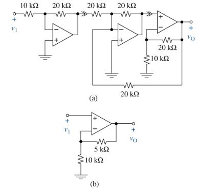
Faced with having to construct the circuit in Figure \(\underline{P}_{4}-46\) (a), a student offers to build the circuit in Figure P4-4 (b) claiming that it performs the same task. As the teaching assistant in the course, do you agree with the student's claim? 10 + 20 6+ + V 20 20 w (3) w
Design a single OP AMP amplifier with a voltage gain of -2500 and an input resistance greater than \(3 \mathrm{k} \Omega\) using standard \(5 \%\) resistance values not greater than \(10 \mathrm{M} \Omega\).
Design an OP AMP amplifier with a voltage gain of 5 using only \(15-\mathrm{k} \Omega\) resistors and one OP AMP.
Using a single OP AMP, design a circuit with inputs \(v_{1}\) and \(v_{2}\) and an output \(v_{\mathrm{O}}=v_{2}-5 v_{1}\). The input resistance seen by each input should be greater than \(1 \mathrm{k} \Omega\).
(a) Using two OP AMPs, design an OP AMP circuit with inputs \(v_{1}, v_{2}\), and \(100 \mathrm{mV}\) and an output of \(v_{\mathrm{O}}=-3 v_{1}+2\) \(v_{2}-300 \mathrm{mV}\).(b) Assuming that you can invert any input, repeat the design using only one OP AMP.
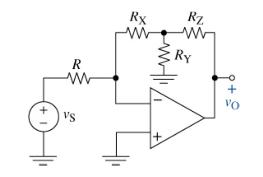
The OP AMP circuit shown in Figure P4=51 has the following input-output relationship:\[v_{\mathrm{O}}=-\frac{\left(R_{\mathrm{X}} R_{\mathrm{Y}}+R_{\mathrm{X}} R_{\mathrm{Z}}+R_{\mathrm{Y}} R_{\mathrm{Z}}ight)}{R R_{\mathrm{Y}}} v_{\mathrm{S}}\]\(R_{\mathrm{Y}}\) was accurately measured to be
Design a cascaded OP AMP circuit that will produce the output \(v_{\mathrm{O}}=25 \times 10^{9} v_{\mathrm{S}}+2.5 \mathrm{~V}\). The maximum gain for the OP AMPs available is 10,000. The input stage must have an input resistance of \(1 \mathrm{k} \Omega\) or greater. Because of the high gain,
Design a cascaded OP AMP circuit that will produce the following output \(v_{\mathrm{O}}=-3.5 \times 10^{6} v_{\mathrm{S}}-1.5 \mathrm{~V}\). The maximum gain for an OP AMP is 10,000. The input stage must have an input resistance of \(1 \mathrm{k} \Omega\) or greater. The only voltage source
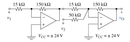
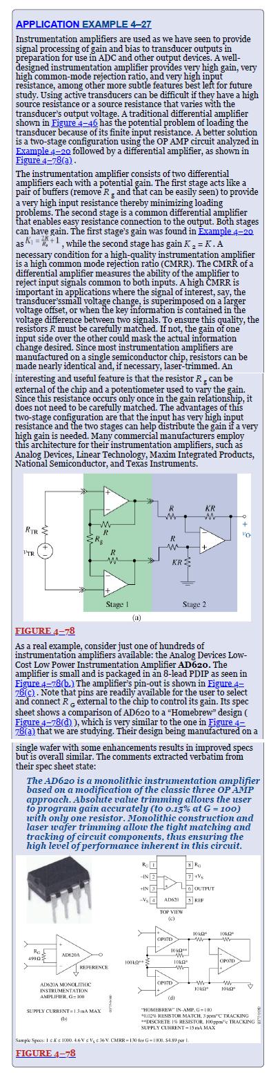
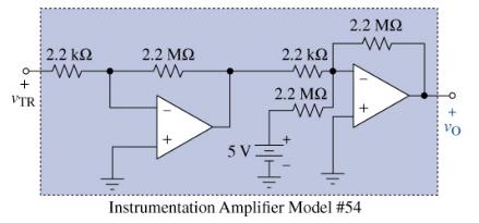
Using the instrumentation amplifier shown in Figure 4=78 ( Example 4-27), design a circuit that will produce the output \(v_{\mathrm{O}}=5 \times 10^{5}\left(v_{1}-v_{2}ight)\). No single OP AMP can have a gain greater than 5000 . APPLICATION EXAMPLE 4-27 Instrumentation amplifiers are used as we
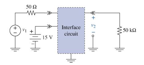
Design the interface circuit in Figure P4=55 so that the output is \(v_{2}=10^{4} v_{1}-5.0 \mathrm{~V}\). +1 50 V1 + 15 V Interface circuit V+A V2 50
(a) Design a circuit that can produce \(v_{\mathrm{O}}=2000 v_{\mathrm{TR}}-\) 2.6 V using two OP AMPs. The input resistance must be greater than \(10 \mathrm{k} \Omega\). for \(v_{\mathrm{TR}}\). The largest resistor you can use is \(1 \mathrm{M} \Omega\).(b) Repeat using only one OP AMP. What
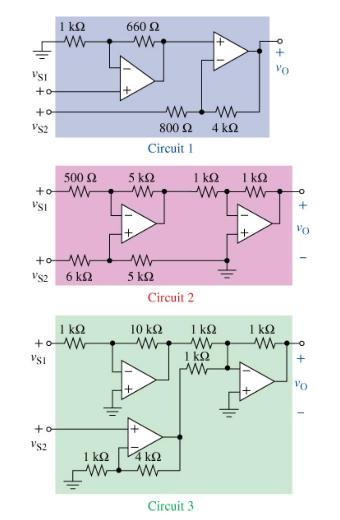
A requirement exists for an OP AMP circuit with the input-output relationship\[v_{\mathrm{O}}=10 v_{\mathrm{S} 1}-5 v_{\mathrm{S} 2}\]Three proposed designs are shown in Figure P4=57. As the project engineer, you must recommend one of these circuits for production. Which of these circuits would you
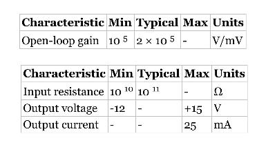
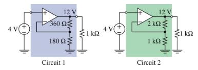
A requirement exists for an OP AMP circuit to deliver \(12 \mathrm{~V}\) to a \(1-\mathrm{k} \Omega\) load using a \(4-\mathrm{V}\) source as an input voltage. Two proposed designs are shown in Figure P4=58 . Some characteristics of the OP AMP that must be used in the design are as follows:Which of
The analog output of a five-bit DAC is \(2.8125 \mathrm{~V}\) when the input code is \((1,0,0,1,0)\). What is the full-scale output of the DAC? How much does the analog output change when the input LSB changes?
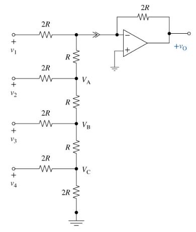
An \(R-2 R\) DAC is shown in Figure P4-60. The digital voltages \(v_{1}, v_{2}\), etc., can be either \(5 \mathrm{~V}\) for a logic 1 or \(\mathrm{O} \mathrm{V}\) for a logic 0 . What is the DAC's output when the logic input is \((1,1,0\), \(1)\) ? + 6+ 5 V2 + V3 5 +9 VA 2R www 2R ww 2R W 2R ww R R
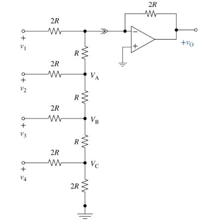
A fifth bit is added to the \(R-2 R\) DAC shown in Figure \(\mathrm{P} 4-60\). What is the aximum possible magnitude of the output voltage? What is the resolution of the revised DAC? + V 5 +0 V2 + V3 6 + VA 2R www 2R ww 2R www 2R ww R R R 2R w ww www www VA VB Vc 2R W +v0
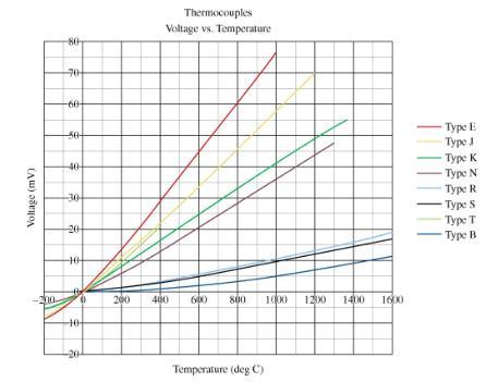
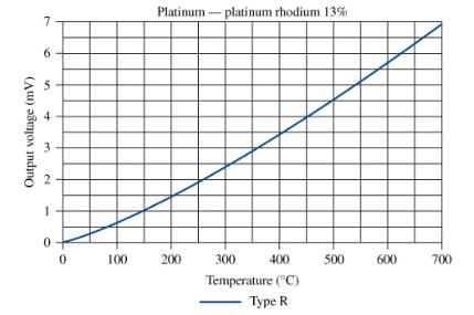
(a) An iron-copper nickel (Fe-CuNi) thermocouple (Type J) needs to be used to measure temperatures between \(200^{\circ} \mathrm{C}\) and \(1200^{\circ} \mathrm{C}\). Its output will be used as an input to an \(\mathrm{ADC}\) with a \(0-5 \mathrm{~V}\) input. The characteristics of various
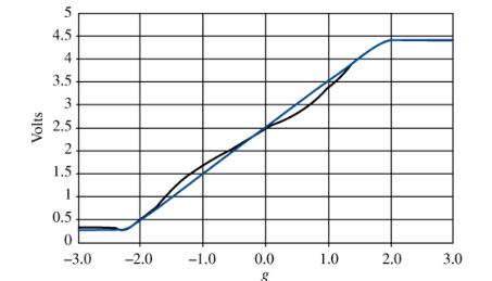
An analog accelerometer produces a continuous voltage that is proportional to acceleration in gravitational units or \(\mathrm{g}\). Figure P4-63 shows the characteristics of the accelerometer in question. The curvy trace is the actual characteristics; the straight trace is an acceptable linearized
A commercial delivery drone needs a small pressure transducer to measure its altitude. A particular sensor is found that meets the basic specs. It can measure pressures of \(15 \mathrm{kPa}\) (2.18 psi) to \(115 \mathrm{kPa}(16.8 \mathrm{psi})\) linearly. It requires \(5 \mathrm{~V}\) to operate,
A medical grade pressure transducer has been developed for use in invasive blood pressure monitoring. The output voltage of the transducer is \(v_{\mathrm{TR}}=(0.06 P-0.75) \mathrm{mV}\), where \(P\) is pressure in \(\mathrm{mmHg}\). The output resistance of the transducer is \(1 \mathrm{k}
The acid/alkaline balance of a fluid is measured by the \(\mathrm{pH}\) scale. The scale runs from \(\mathrm{o}\) (extremely acid) to 14 (extremely alkaline), with \(\mathrm{pH} 7\) being neutral. A pH electrode is a sensor that produces a small voltage that is directly proportional to the
Your engineering firm needs an instrumentation amplifier that provides the following input-output relationship: \(v_{\mathrm{O}}=10^{6} v_{\mathrm{TR}}-3.5 \mathrm{~V}\). The transducer is modeled as a voltage source in series with a resistor that varies with the transducer voltage from \(50
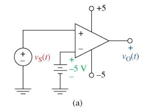
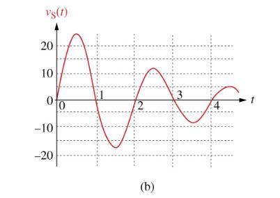
A signal vS(t)vS(t) is fed into the circuit as shown in Figure P4-68. Plot the output vO(t)vO(t). +1 vs(1) + -5 V I (a) Q+5 6-5 Vo(t)
A rocket design team has a need to detect the temperatures in a rocket motor. The combustion chamber is that part of a thrust chamber where the combustion of the propellant takes place. The combustion temperature is much higher than the melting points of most chamber wall materials and reaches a
The OP AMP in Figure P4=70 operates as a comparator. Find the output voltage when \(v_{\mathrm{S}}=9 \mathrm{~V}\). Repeat for \(v_{\mathrm{S}}=-3 \mathrm{~V}\) and \(v_{\mathrm{S}}=12 \mathrm{~V}\). 2R ww VS +12 V R ww + VO
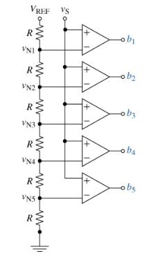
A five-bit flash \(\mathrm{ADC}\) in Fi gure \(\mathrm{P} 4-71\) uses a reference voltage of \(5 \mathrm{~V}\). Find the output code for the analog inputs \(v_{\mathrm{S}}=\) \(3.5 \mathrm{~V}, 2.3 \mathrm{~V}\), and \(4.9 \mathrm{~V}\). If the reference voltage is changed to \(8 \mathrm{~V}\),
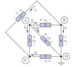
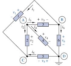
In Figure P2-14 \(v_{2}=30 \mathrm{~V}, v_{3}=-20 \mathrm{~V}\), and \(v_{4}\) \(=6 \mathrm{~V}\). Find \(v_{1}, v_{5}\), and \(v_{6}\). X + 1 4 5 Vs+ B 16 6 V6 D
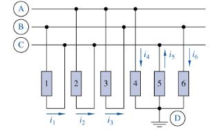
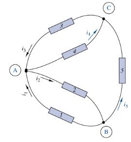
The circuit in Figure P2-16 is organized around the three signal lines A, B, and C.(a) Identify the nodes and at least five loops in the circuit.(b) Write KCL connection equations for the circuit.(c) If \(i_{1}=-30 \mathrm{~mA}, i_{2}=-18 \mathrm{~mA}\), and \(i_{3}=75 \mathrm{~mA}\), find \(i_{4},
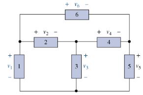
(a) Are any of the elements in Figure P2-17 in series or parallel? If so, identify the ones that are.(b) Then if \(v_{2}=10 \mathrm{~V}, v_{4}=10 \mathrm{~V}\), and \(v_{5}=5 \mathrm{~V}\), find \(v_{1}, v_{3}\), and \(v_{6}\).(c) Suppose that element 3 becomes shorted, i.e., \(v_{3}=\mathrm{oV}\).
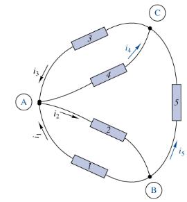
Are any of the elements in Figure P2-18 in series or parallel? If so, identify the ones that are. Then if \(i_{1}=-5 \mathrm{~mA}, i_{2}\) \(=10 \mathrm{~mA}\), and \(i_{3}=-15 \mathrm{~mA}\), find \(i_{4}\) and \(i_{5}\). A B
(a) Use the passive sign convention to assign voltage variables consistent with the currents in Figure \(\mathrm{P}_{2}-18\). Write three KVL connection equations using these voltage variables.(b) If \(v 5=0 \mathrm{~V}\), what can be said about the voltages across all the other elements? A P B
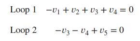
The KVL equations for a two-loop circuit are:Draw the circuit diagram and indicate the reference directions for the element voltages. Loop 1 Loop 2 U + V + V3 + V = 0 -V3 V4 + U5 = 0
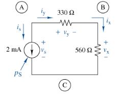
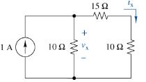
For the circuit in Figure P2-21, write a complete set of connection and element constraints and then find \(i_{\mathrm{x}}, v_{\mathrm{x}}\), and \(p_{\mathrm{S}}\). A 2 mA PS +1 330 + Py C 560 ( B
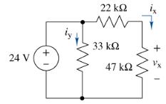
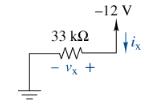
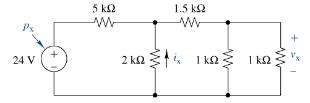
Find \(v_{\mathrm{x}}\) and \(i_{\mathrm{x}}\) in Figure P2-22 . Remove the \(33-\mathrm{k} \Omega\) resistor and repeat. What effect did removing the \(33-\mathrm{k} \Omega\) resistor have on \(v_{\mathrm{x}}\) and \(i_{\mathrm{x}}\) ? Did the power supplied by the source change? 24 V + 22 www
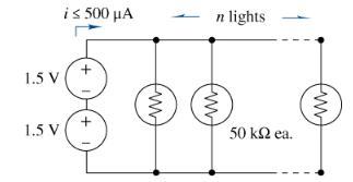
A modeler wants to light his model building using miniature grain-of-wheat light bulbs connected in parallel as shown in Figure P2-23 . He uses two 1.5-V "C-cells" to power his lights. He wants to use as many lights as possible but wants to limit his current drain to \(500 \mu \mathrm{A}\) to
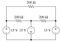
In Figure P2-24:(a) Assign a voltage and current variable to every element.(b) Use KVL to find the voltage across each resistor.(c) Use Ohm's law to find the current through each resistor.(d) Use KCL to find the current through each voltage 200 |15 V 15 V 200 ( 200 15 V ( +
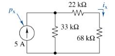
Find the power provided by the source and the current through the \(68-\mathrm{k} \Omega\) resistor in Figure \(\mathrm{P}_{2}-25\). Px. 5 A 22 33 68
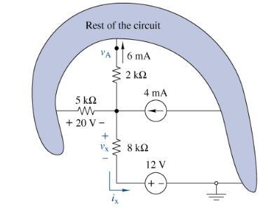
Figure P2-26 shows a subcircuit connected to the rest of the circuit at four points.(a) Use element and connection constraints to find \(v_{\mathrm{x}}\) and \(i\) \(x\).(b) Show that the sum of the currents into the rest of the circuit is zero.(c) Find the voltage \(v_{\mathrm{A}}\) with respect
Figure \(\mathrm{P}_{2}-27\) shows a resistor with one terminal connected to ground and the other connected to an arrow. The arrow symbol is used to indicate a connection to one terminal of a voltage source whose other terminal is connected to ground. The label next to the arrow indicates the
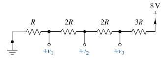
A circuit similar to the one shown in Figure \(\mathrm{P}_{2}-28\) is used in flash comparator circuits studied later. Find the voltages \(v_{1}\), \(v_{2}\), and \(v_{3}\). R ww +11 2R +12 2R www +V3 3R www 8V
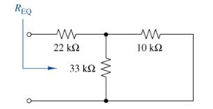
Find the equivalent resistance \(R_{\text {EQ }}\) in Figure \(\mathrm{P}_{2}-\) 29. REQ 22 33 www 10
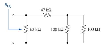
Find the equivalent resistance \(R_{\mathrm{EQ}}\) in Figure \(\mathrm{P}_{2}=3 \underline{\mathrm{O}}\). REQ 63 47 100 100
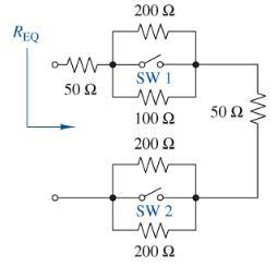
Figure \(\mathrm{P}_{2}-31\) shows a circuit with two switches.(a) How would you select the switches (open or closed) to achieve an \(R_{\mathrm{EQ}}\) of \(167 \Omega\) ?(b) How would you select the switches (open or closed) to achieve an \(R_{\mathrm{EQ}}\) of \(100 \Omega\) ?(c) How would you
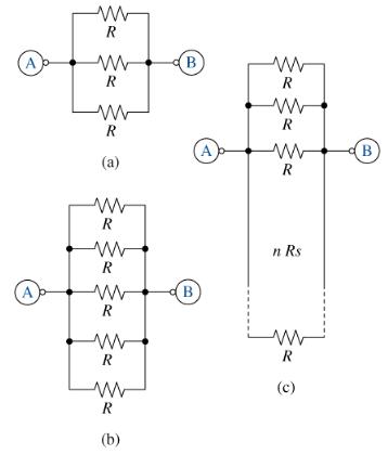
Find \(R_{\mathrm{EQ}}\) between nodes \(\mathrm{A}\) and \(\mathrm{B}\) for each of the circuits in Figure P2-32. What conclusion can you draw about resistors of the same value connected in parallel? www R ww R ww R (a) ww R ww R www R www R ww R (b) B) ( B ww R R ww R n Rs www R (c) B
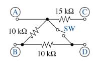
In Figure \(\mathrm{P}_{2}-33\) find the equivalent resistance between terminals \(\mathrm{A}-\mathrm{B}, \mathrm{A}-\mathrm{C}, \mathrm{A}-\mathrm{D}, \mathrm{B}-\mathrm{C}, \mathrm{B}-\mathrm{D}\), and \(\mathrm{C}-\mathrm{D}\) when the switch is open. Repeat for when the switch is closed. (A) 10
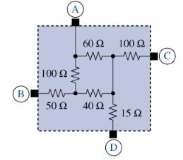
In Figure \(\mathrm{P}_{2}-34\) find the equivalent resistance between terminals \(\mathrm{A}-\mathrm{B}, \mathrm{A}-\mathrm{C}, \mathrm{A}-\mathrm{D}, \mathrm{B}-\mathrm{C}, \mathrm{B}-\mathrm{D}\), and \(\mathrm{C}-\mathrm{D}\). 3001: B 50 A 60 ww 40 100 D 15 C
Using no more than four 1-k \(\Omega\) resistors, all but one of the following equivalent resistors can be constructed: 1 \(\mathrm{k} \Omega, 2 \mathrm{k} \Omega, 500 \Omega, 1.5 \mathrm{k} \Omega, 2.5 \mathrm{k} \Omega, 3 \mathrm{k} \Omega, 333 \Omega, 250 \Omega, 1.33 \mathrm{k} \Omega\), \(2.33
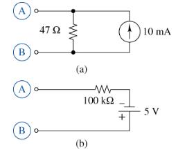
Do a source transformation at terminals A and B for each practical source in Figure P2-3 \(\underline{6}\). B 4792 A) o B (a) www 100 (b) + 10 mA 5 V
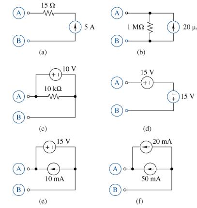
Find the equivalent circuit at terminals \(\mathrm{A}-\mathrm{B}\) for each of the circuits shown in Figure P2-37. A B A Bo A)o Bo 1592 ww (a) 10 (c) +1 ww (+1) (e) 10 V 15 V 10 mA 5 A B B A Bo 1 (b) www 15 V +1 (f) (d) 50 mA +1. 20 mA 20 15 V
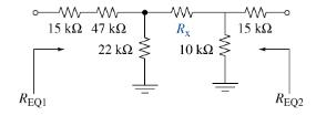
In Figure P2-38 select a value for \(R_{\mathrm{X}}\) so that \(R_{\mathrm{EQ} 1}=\) \(73 \mathrm{k} \Omega\). Then find \(R_{\mathrm{EQ} 2}\) - 15 47 REQI 22 Ri 10 ww 15 REQ2
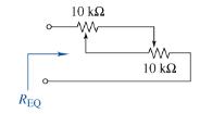
Two 10-k \(\Omega\) potentiometers (a variable resistor whose value between the two ends is \(10 \mathrm{k} \Omega\) and between one end and the wiper-the third terminal-can range from \(0 \Omega\) to \(10 \mathrm{k} \Omega\) ) are connected as shown in Figure P2-39. What is the range of \(R\) EQ?
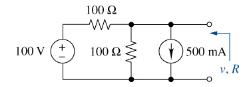
Find the equivalent practical voltage source of the circuit shown in Figure P2-40. 100 (+ V 100 100 1500 mA v. R
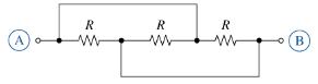
Find the equivalent resistance between terminals \(A\) and \(B\) in Figure P2-41. R www R www R ww (B
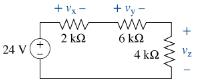
Use voltage division in Figure P2-42 to find \(v_{\mathrm{x}}, v_{\mathrm{y}}\), and \(v_{\mathrm{z}}\) : Then show that the sum of these voltages equals the source voltage. 24V +Vx w + 4
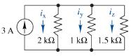
Use current division in Figure P2-43 to find \(i_{\mathrm{x}}, i\) \(y\), and \(i_{z}\). Then show that the sum of these currents equals the source current. 3A i 1.5
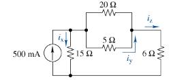
Find \(i_{\mathrm{x}}, i_{\mathrm{y}}\), and \(i_{\mathrm{z}}\) in Figure P2-44. 500 mA USI3 202 50 59 ww
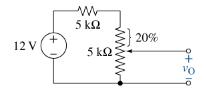
Find \(v_{O}\) in the circuit of Figure P2-45. 12 V ww 5 5 5 20% 9+819
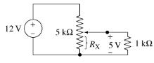
You wish to drive a 1-k \(\Omega\) load from your car battery as shown in Figure P2-46. The load needs \(5 \mathrm{~V}\) across it to operate correctly. Where should the wiper on the potentiometer be set ( \(R_{\mathrm{x}}\) ) to obtain the desired output voltage? 12V 5 + Rx 5V SV
Design a circuit that will deliver \(3 \mathrm{~V} \pm 5 \%\) to a \(1-\mathrm{k} \Omega\) load from a \(10-\mathrm{V}\) source. The practical source has a \(50-\Omega\) series resistor. The load needs at least \(1 \mathrm{~mA}\) to function properly. Use \(\pm 5 \%\) resistors from Appendix G in
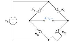
Figure \(\mathrm{P}_{2}-4 \underline{8}\) shows a voltage bridge circuit, that is, two voltage dividers in parallel with a source \(v_{\mathrm{S}}\). One resistor \(R_{\mathrm{X}}\) is variable. The goal is often to "balance" the bridge by making \(v_{\mathrm{x}}=\mathrm{OV}\). Derive an expression
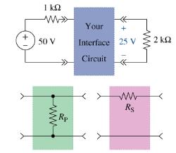
Consider the circuit in Figure P2-49. The task is to deliver \(25 \mathrm{~V}\) to the load. For each of the two interfaces provided, determine the value of \(R_{\mathrm{P}}\) or \(R_{\mathrm{S}}\) needed to deliver the desired voltage to the load. Which interface results in the least power needed
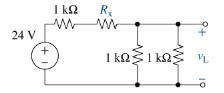
Select a value of Rx in the circuit of Figure P2–50 so that νL = 4 V. Validate your answerusing Multisim. 24 V + ww R ww VL 10
Use circuit reduction to find \(v_{\mathrm{x}}\) and \(i_{\mathrm{x}}\) in Figure \(\underline{\mathrm{P}_{2}-5 \underline{1}}\). 1 102 + Vx 15 Www 10
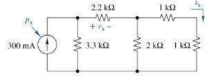
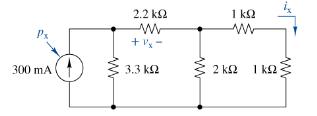
Use circuit reduction to find \(v_{\mathrm{x}}, i_{\mathrm{x}}\), and \(p_{\mathrm{x}}\) in Figure P2-52. Repeat using Multisim. P 300 mA 2.2 + 3.3 1 2 www
Use circuit reduction to find \(v_{\mathrm{x}} i_{\mathrm{x}}\), and \(p_{\mathrm{x}}\) in Figure P2-53. 24 V 5 2 1.5 ww
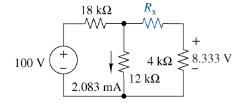
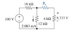
Find \(R_{\mathrm{X}}\) in the circuit of Figure \(\mathrm{P}_{2}-54\). 100 V 18 ww 2.083 mA R + 4 8.333 V 12
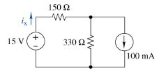
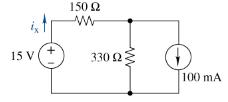
Use source transformation to find \(i_{\mathrm{x}}\) in Figure \(\underline{\mathrm{P}_{2}-55 \text {. }}\) 15V/ +1 150 330 (100) mA
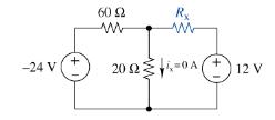
Select a value for \(R_{\mathrm{x}}\) so that \(i_{\mathrm{x}}=\mathrm{O}\) A in Figure P2-5 6 . -24 V 60 2 ww Rx ww 20024-0A( 12 V
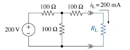
The current through \(R_{\mathrm{L}}\) in Figure \(\mathrm{P}_{2}-57\). is \(200 \mathrm{~mA}\). Use source transformations to find \(R_{\mathrm{L}}\). Validate your answer using Multisim. 200 V (+ 100 100) 100 4 = 200 mA R
The box in the circuit in Figure \(\mathrm{P}_{2}-5 \underline{8}\) is a resistor, \(R_{\mathrm{X}}\), whose value can be anywhere between \(100 \Omega\) and \(1 \mathrm{M} \Omega\).(a) Use circuit reduction to find the range of values of \(v_{\mathrm{X}}\).(b) Use Multisim's "Parameter Sweep"
Use Multisim to find all the currents and voltages in the circuit of Figure P2–54. 100 V + 18 2.083 mA R + 4 8.333 V 12
Use Multisim to find all the currents and voltages in the circuit of Figure P2–55. 15 V ( + 150 330 } 100 mA
Use Multisim to find ix, vx, and px in the circuit of Figure P2–52. 300 mA ( 2.2 + 3.3 ww 1
Showing 4300 - 4400
of 5433
First
37
38
39
40
41
42
43
44
45
46
47
48
49
50
51
Last
Step by Step Answers