New Semester
Started
Get
50% OFF
Study Help!
--h --m --s
Claim Now
Question Answers
Textbooks
Find textbooks, questions and answers
Oops, something went wrong!
Change your search query and then try again
S
Books
FREE
Study Help
Expert Questions
Accounting
General Management
Mathematics
Finance
Organizational Behaviour
Law
Physics
Operating System
Management Leadership
Sociology
Programming
Marketing
Database
Computer Network
Economics
Textbooks Solutions
Accounting
Managerial Accounting
Management Leadership
Cost Accounting
Statistics
Business Law
Corporate Finance
Finance
Economics
Auditing
Tutors
Online Tutors
Find a Tutor
Hire a Tutor
Become a Tutor
AI Tutor
AI Study Planner
NEW
Sell Books
Search
Search
Sign In
Register
study help
computer science
systems analysis design
The Analysis And Design Of Linear Circuits 10th Edition Roland E. Thomas, Albert J. Rosa, Gregory J. Toussaint - Solutions
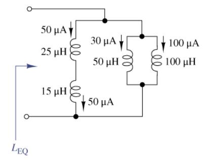
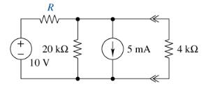
What is the equivalent inductance and initial current for the inductors shown in Figure P6-42? LEQ 50 . .. 25 15 1 30 . . | 50 150 S | 100 100
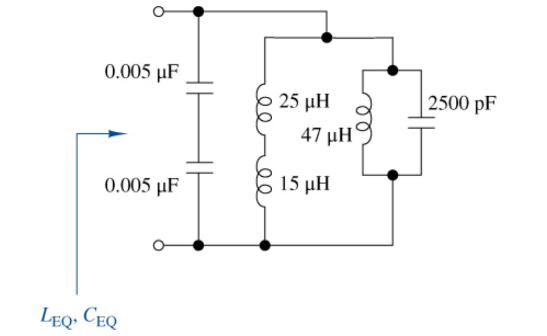
For the circuit in Figure P6-43, find an equivalent circuit consisting of one inductor and one capacitor. Select a value of an inductor and a capacitor from among the standard values in Appendix G to realize your result and connect them appropriately. 0.005 0.005 LEQ, CEQ 25 47 15 2500 pF
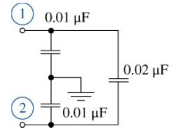
Figure P6-44 is the equivalent circuit of a two-wire feedthrough capacitor.(a) What is the capacitance between terminal 1 and ground when terminal 2 is open?(b) What is the capacitance between terminal 1 and ground when terminal 2 is grounded? 10.01 F 2 0.01 F 0.02 F
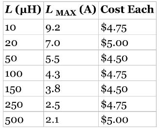
A switching power supply requires an inductor that can store at least \(1 \mathrm{~mJ}\) of energy. A list of available inductors is shown below. Select the inductor that best meets the requirement. Consider both meeting the specifications and cost. Explain your choice. L (H) L MAX (A) Cost Each 10
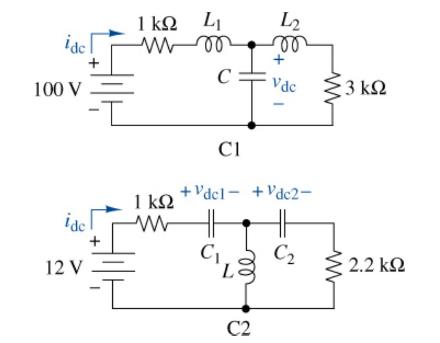
The circuits in Figure P6-46 are driven by dc sources. Find the current through the source and the voltages across the capacitors. ide 100 V ide 12 V + + -I 1k L M00 m 1 C CI +Vdcl +Vdc2- C L3 L 800 Vdc C2 C 3 2.2
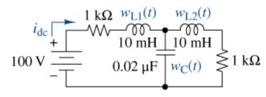
The circuit in Figure P6-4.7 is driven by a 100-V dc source. Find the energy stored in the capacitor and each inductor under dc conditions. ide 100 V + WL2(1) mo 10 mH | 10 mH 0.02 F | wc(t) 1k WL (1) WL1(1) M00
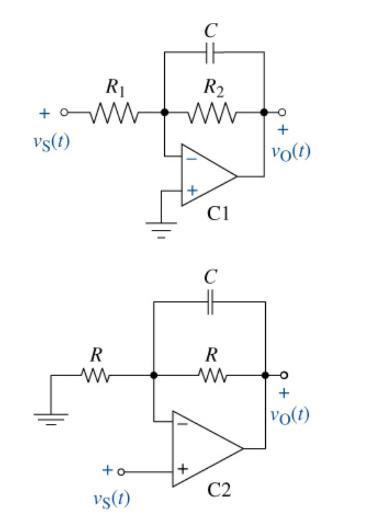
(a) The OP AMP circuits in Figure P6-48 have capacitors in their feedback loops. Determine the circuit gains at dc and as the frequency approaches \(\infty \mathrm{rad} / \mathrm{s}\).(b) Replace the capacitors with inductors and repeat (a). R R +WWW M vs(t) R ww +0 Vs(1) C + C1 C R C2 + Vo(t) +
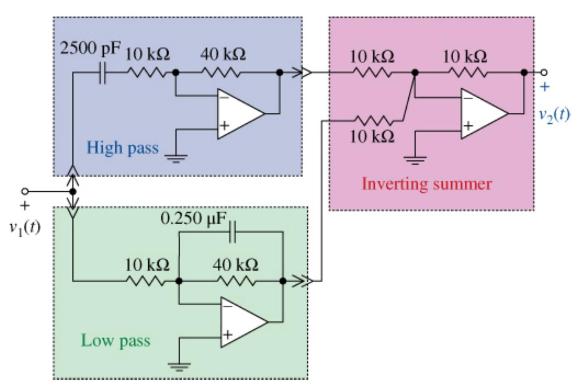
The OP AMP circuit shown in Figure P6-4.9 is a band (reject filter that will be studied later. Determine the circuit gain at dc and as the frequency approaches \(\infty \mathrm{rad} / \mathrm{s}\). V (1) 2500 pF 10 High pass 10 Low pass 40 0.250 F, 40 10 10 10 Inverting summer V3(1)
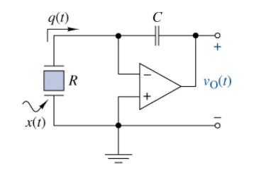
Piezoelectric transducers (sensors) measure dynamic phenomenasuchaspressureand force. Thesephenomenacause stresses that "squeeze" a quantity of electric charge from piezoelectric material in the transducer (the term piezo means "squeeze" in Greek). The amount of charge \(q(t)\) is directly
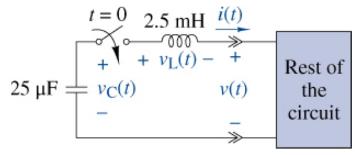
At t=0t=0, the switch in Figure P6-51 is closed and thereafter the voltage across the capacitor isvC(t)=(10+10,000t)e−8000t VvC(t)=(10+10,000t)e−8000t VUse MATLAB to solve all of the following problems.(a) Use the capacitor's i−vi−v characteristic to find the current i(t)i(t) for
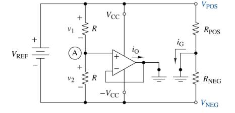
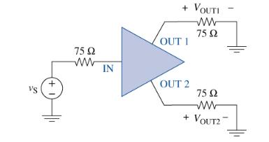
The circuit in Figure P4-72 produces bipolar power supply voltages \(V_{\text {POS }}>0\) and \(V_{\text {NEG }}0\). Note that the OP AMP output is grounded and that its \(+V_{\mathrm{CC}}\) and \(-V_{\mathrm{CC}}\) terminals are connected to \(V_{\mathrm{POS}}\) and \(V\) NEG , respectively.(a)
Electric Scooter Governor A town has a new light rail system. To encourage its use, the town council approved installing electric scooters at each station for riders to rent cheaply to take them to their final destinations. The town hired a small start-up company to provide location finding and
A particular pressure sensor is designed to operate under constant pressure. The task is to detect a pressure increase and sound an alarm. The sensor produces \(1 \mathrm{mV}\) at \(100 \mathrm{psi}\), its usual operating pressure, and increases by \(1 \mu \mathrm{V} / \mathrm{psi}\). The design
A weathervane turns with the wind direction. The base of the weathervane is connected to a rotary potentiometer without stops, that is, the potentiometer turns from o \(\Omega\) to \(10 \mathrm{k} \Omega\) linearly clockwise, but jumps to \(0 \Omega\) after the maximum resistance is reached and
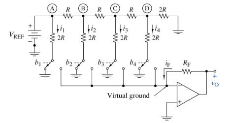
The circuit in Figure P4=76 is a four-bit DAC. The DAC output is the voltage \(v_{\mathrm{O}}\) and the input is the binary code represented by bits \(b_{1}, b_{2}, b_{3}\), and \(b_{4}\). The input bits are either \(\mathrm{o}\) (low) or 1 (high), and each controls one of the four switches in the
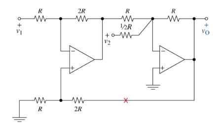
(a) A Find the input-output relationship of the circuit in Figure \(\mathrm{P}_{4}=77\).(b) Design a circuit that realizes the relationship found in part (a) using only \(15-\mathrm{k} \Omega\) resistors and one OP AMP.(c) (A) The wire fails (opens) at the \(W\), what is the output then? +5 R ww ww
Strain gauges measuring the deflection of a sintered metal column are connected to a Wheatstone bridge. The output of the bridge is balanced when there is no strain producing o \(\mathrm{V}\) output. As the column is deflected, the bridge produces \(150 \mu \mathrm{V} / 22\) change caused by the
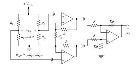
A strain gauge with an unstressed resistance of \(120 \Omega\) is used in a bridge as shown in Figure P4=79. The reference voltage is +25 \(\mathrm{V}\). When fully stressed the resistance of the strain gauge is \(\mathbf{1 2 0 . 1}\) \(\Omega\). There is a need to design an instrumentation
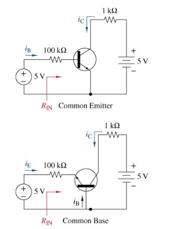
Figure P4-80 shows two circuits using the same transistor connected in different ways. The transistor has a \(\beta\) of 90 and a \(V\) \(\gamma\) of \(0.7 \mathrm{~V}\). Find the current gain of each circuit \(i_{\mathrm{C}} / i_{\mathrm{B}}\) for the common emitter and \(i_{\mathrm{C}} /
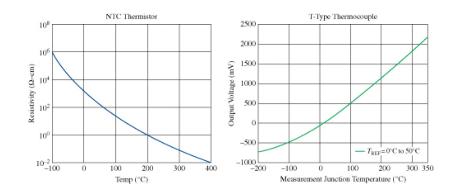
As a young designer at a firm that builds lithium batteries, you are tasked with designing a sensor system that displays the temperature inside the battery pack. The range of temperatures that need to be displayed is from \(0^{\circ} \mathrm{C}\) to \(200^{\circ} \mathrm{C}\). The output will be to
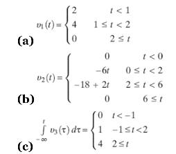
Sketch the following waveforms:(a) \(v_{1}(t)=u(t)-u(t-3) \mathrm{V}\)(b) \(v_{2}(t)=5 u(t+1)-5 u(t-2) \mathrm{V}\)(c) \(i_{3}(t)=-2 u(t)-u(t-1)+3 u(t-2) \mu \mathrm{A}\)(d) \(i_{4}(t)=10 u(-t) \mathrm{mA}\)
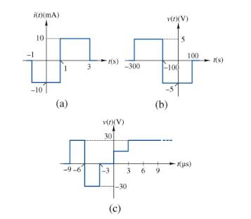
Using appropriate step functions, write an expression for each waveform in Figure P \(5=\). i(t)(mA) 10 -10 1 (a) 3 t(s) -300 Y(7)(V) 30 L 30 3 6 v(r)(V) -100 (b) 5 100 -(us) - 1(s)
Sketch the following waveforms:(a) \(v_{1}(t)=12-2 u(t) \mathrm{V}\)(b) \(i_{2}(t)=-2 u(t+0.003)+2 u(t-0.003) \mu \mathrm{A}\)(c) \(v_{3}(t)=t[u(t-1)-u(t-2)] \mathrm{mV}\)(d) \(i_{4}(t)=5 u(-t) \mathrm{A}\)
Sketch the following waveforms:(a) \(v_{1}(t)=r(t+2)-r(t-2) \mathrm{V}\)(b) \(v_{2}(t)=4+r(t+1)-2 r(t-1)+r(t-3) \mathrm{V}\)(c) \(v_{3}(t)=\frac{d v_{1}(t)}{d t}\)(d) \(v_{4}(t)=\frac{d^{2} v_{2}(t)}{d t^{2}}\)
Express each of the following signals as a sum of singularity functions. (a) (b) (c) in(t)=4 0 (1)= 0 1
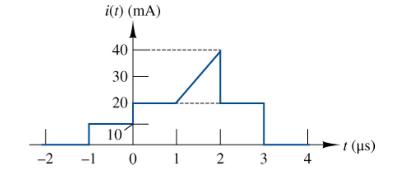
Express the waveform in Figure P5 5 as a sum of singularity functions. -2 -1 i(t) (mA) 40 30 20 101 0 I 1 2 3 4 t (s)
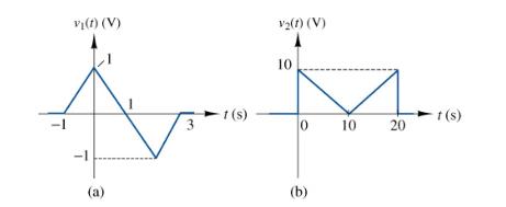
Express each of the waveforms in Figure P \(5=7\) as a sum of singularity functions. V (1) (V) -1 (a) 3 1 (s) V/(1) (V) 10 0 (b) 10 20 t (s)
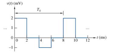
Using its pulse voltage source, generate on Multisim a waveform \(v(t)\) that starts at \(t=1 \mathrm{~ms}\) and consists of a pulse train of \(5-\mathrm{V}\) pulses with a \(2-\mathrm{ms}\) pulse width that repeat every 8 \(\mathrm{ms.}\) Display two full pulses.
Sketch the following exponential waveforms. Find the amplitude and time constant of each waveform.(a) \(v_{1}(t)=5 e^{-2 t} u(t) \mathrm{V}\)(b) \(v_{2}(t)=5 e^{-2 t} u(t-1) \mathrm{V}\)(c) \(v_{3}(t)=5 e^{-2(t-1)} u(t) \mathrm{V}\)(d) \(v_{4}(t)=5 e^{-2(t-1)} u(t-1) \mathrm{V}\)
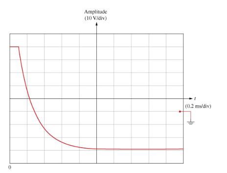
In the lab, you see the waveform on the oscilloscope shown in Figure P5-10. Write an expression for the waveform. Note that \(t=0\) is on the far-left side of the display. 0 Amplitude (10 V/div) (0.2 ms/div)
Half-life, \(t_{1 / 2}\), is the time required for a quantity to shrink to half its initial value. Radioactive elements are often defined by their half-life radioactive decay given by \(N(t)=N_{0} e^{-\frac{t}{\tau}}\), where \(N_{\mathrm{O}}\) is the initial quantity and \(\tau\) is the element's
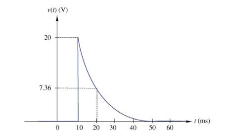
Write an expression for the waveform in Figure P5-12 . v(1) (V) 20 7.36 0 10 20 30 40 50 60 1 (ms)
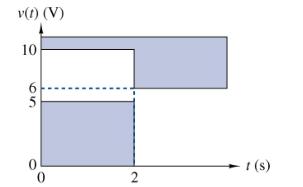
Design an exponential waveform that fits entirely within the nonshaded region in Figure P \(5=13\). v(t) (V) 10 6 0 0 2 t(s)
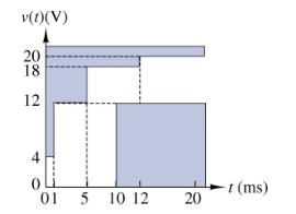
Design an exponential waveform that fits entirely within the nonshaded region in Figure P5-14. y(t)(V) 20 18 12 4 0 01 5 10 12 20 -I (ms)
Find the period, frequency, amplitude, time shift, and phase angle of the following sinusoids.(a) \(v_{1}(t)=240 \cos (120 \pi t)-240 \sin (120 \pi t) \mathrm{V}\)(b) \(v_{2}(t)=-30 \cos (50 \mathrm{k} \pi t)+40 \sin (50 \mathrm{k} \pi t) \mathrm{V}\)
(a) Plot the waveform of each sinusoid in Problem 5-15 by hand.Data From Problem 5-15Find the period, frequency, amplitude, time shift, and phase angle of the following sinusoids.(b) Use Multisim to produce the waveform in Problem 515 (a).Data From Problem 5-15(a) \(v_{1}(t)=240 \cos (120 \pi
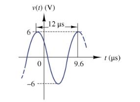
Write an expression for the sinusoid in Figure P \(5=17\). What are the phase angle and time shift of the waveform? v(1) (V) 0 12 us. 9.6 t (s)
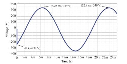
Write an expression for the sinusoid in Figure P \(5=-18\). What are the phase angle and time shift of the waveform? Voltage (V) 400 300 200 100 0 -100 -200 -300 -400 0 (0 s.-237 V)- (6.25 ms, 339 V) (22.9 ms. 339 V). 2m 4m 6m 8m 10m 12m 14m 16m 18m 20m 22m 24m Time (s)
Find the Fourier coefficients, cyclic frequency, and radian frequency of the following sinusoids:(a) \(v(t)=50 \cos \left(100 \pi t+36.9^{\circ}ight) \mathrm{V}\)(b) \(i(t)=240 \cos \left(1200 \pi t-90^{\circ}ight) \mathrm{mA}\)
For the following sinusoid: \(v(t)=10 \cos (2 \pi 200 t+\) \(\left.60^{\circ}ight) \mathrm{V}\)(a) Find the Fourier coefficients, cyclic frequency, and radian frequency.(b) Plot the waveform by hand.(c) Use MATLAB to produce the waveform.(d) Use Multisim to produce the waveform.
Consider the following composite waveforms.(a) \(v_{1}(t)=15\left[1-e^{-25,000 t}ight] u(t) \mathrm{V}\)(a) \(v_{2}(t)=-2\left[e^{-t}-e^{-5 t}ight] u(t) \mathrm{V}\)Sketch each on paper and then generate each using MATLAB and compare the results.
Consider the following composite waveforms.(a) \(i_{1}(t)=10+5 \sin (500 \pi t) u(t) \mathrm{mA}\)(b) \(i_{2}(t)=50\left[e^{-1000 t}+\cos (2000 \pi t)ight] u(t) \mathrm{mA}\)Sketch each by hand and then generate each using MATLAB and compare the results.
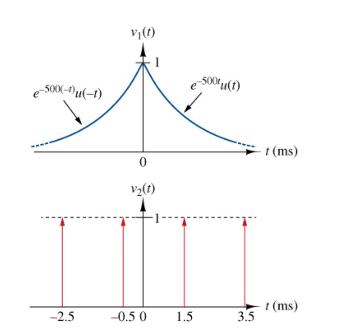
The two signals shown in Figure \(\mathrm{P}_{5}-23\) are multiplied together. Write an expression for their output. -500(-)u(-1) -2.5 Vj(t) 0 V(t) -0.5 0 1.5 -500 u(t) 3.5 - 1 (ms) 1 (ms)
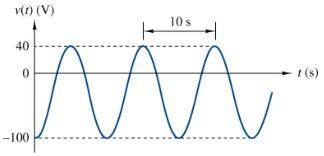
Write an expression for the composite sinusoidal waveform in Figure P \(5=24\). v(1) (V) 40 0 -100 10 s +
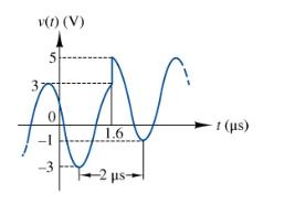
Write an expression for the composite sinusoidal waveform in Figure P \(5=25\). v(1) (V) FAL 1.6 -2 s- 0 t (s)
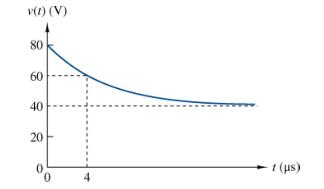
Write an expression for the composite exponential waveform in Figure P5-26. v(t) (V) 80 60 40 20 0. 0 4 -1 (1)
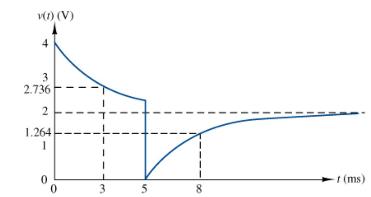
Write an expression for the composite exponential waveform in Figure P5-27. v(1) (V) 4 3 2.736 2 1.264 1 0 0 3 5 8 t (ms)
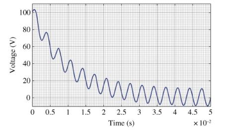
Write an expression for the composite exponential waveform in Figure P \(5=28\). Then use MATLAB to construct the same waveform and compare the results. Voltage (V) 100 80 60 40 20 www. mmmmm 0 0 0.5 1 1.5 1.5 2 2.5 3 3.5 4 4.5 5 Time (s) x 10-2
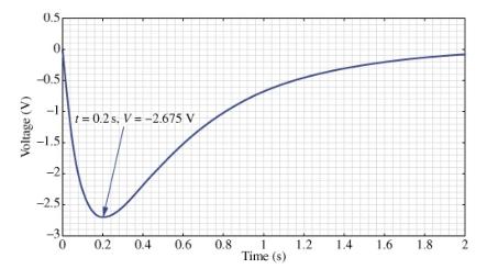
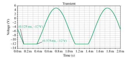
For the double exponential \(v(t)=-5\left[e^{-\alpha t}-e^{-10 t}ight]\) \(u(t) \mathrm{V}\) shown in Figure P 5 -29. , find \(\alpha\). Voltage (V) 0.5 0 -0.5A -1 -1.5 -2.5 -35 0 t = 0.2s, V=-2.675 V 0.2 0.4 0.6 0.8 1 Time (s) 1.2 1.4 1.6 1.8 2
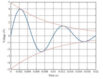
Write an expression for the damped sine waveform in Figure P5=30 . The exponential envelope was added to help in the determination of the damping exponential. Voltage (V) 7 M CE 0 -1 0 0.002 0.004 0.006 0.008 0.01 0.012 0.014 0.016 0.018 002 Time (s)
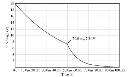
A circuit response is shown in Figure \(P_{5}=31\) that occurs when one exponential stops and another begins where the prior one left off. Determine an approximate expression for the waveform. Voltage (V) 20 18 16 14 12 10 6 4 2 (50.0 ms, 7.34 V) 0.0 10.0m 20.0m 30.0m 40.0m 50.0m 60.0m 70.0m 80.0m
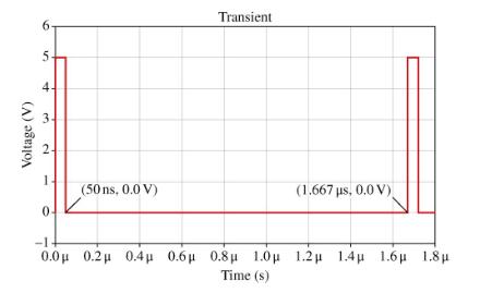
An object-detection radar for a drone sends out the signal shown in Figure P \(5=32\).(a) Write an expression for the first two pulses of the signal.(b) To avoid ambiguity, the radar receiver only accepts one pulse at a time. Considering the time for the pulse to reach an object and return to the
Find \(V_{\mathrm{MAX}}, V_{\mathrm{MIN}}, V_{\mathrm{p}}, V_{\mathrm{pp}}, V_{\text {avg }}\), and \(V_{\mathrm{rms}}\) for each of the following sinusoids.(a) \(v_{1}(t)=84.84 \cos (120 \pi t)+84.84 \sin (120 \pi t) \mathrm{V}\)(b) \(v_{2}(t)=-40 \cos (2000 \pi t)-30 \sin (2000 \pi t)
An exponential waveform given by \(i(t)=250 e^{-1000 t} u(\) \(t\) ) \(\mathrm{mA}\) repeats every five time constants.(a) Find \(I_{\mathrm{p}}, I_{\mathrm{pp}}, I_{\mathrm{MAX}}\), and \(I_{\mathrm{MIN}}\).(b) Find \(I_{\text {avg }}\) and \(I_{\mathrm{rms}}\).(c) Find the period
Find \(V_{\text {MAX }}, V_{\text {MIN }}, V_{\mathrm{p}}, V_{\mathrm{pp}}, V_{\text {avg }}, V_{\mathrm{rms}}\), and \(T_{\mathrm{o}}\) for the periodic waveform in Figure \(\mathrm{P} 5=35\). v(1) (mV) 2 1 0 2 To 4 6 8 10 12 -1 (ms)
Figure \(\mathrm{P}_{5}=36\) is the result of the sum of a fundamental and one of its harmonics (an integer multiple of the fundamental). Find \(V_{\text {MAX }}, V_{\text {MIN }}, V_{\mathrm{p}}, V_{\mathrm{pp}}, V_{\mathrm{avg}}, V_{\mathrm{rms}}\), and \(T\) o for the waveform. 1.5 1.0 0.5 0.0
Figure P \(5=37\) displays the response of a circuit to a square wave signal. The response is a periodic sequence of exponential waveforms. Each exponential has a time constant of \(1.6 \mathrm{~ms}\).(a) Find \(V_{\text {MAX }}, V_{\text {MIN }}, V_{\mathrm{p}}, V_{\mathrm{pp}}\), and
Find \(V_{\text {MAX }}, V_{\text {MIN }}, V_{\text {avg }}\), and \(V_{\text {rms }}\) of the offset sine wave \(v(t)=V_{\mathrm{O}}+V_{\mathrm{A}} \cos \left(2 \pi t / T_{\mathrm{o}}ight) \mathrm{V}\) in terms of \(V_{\mathrm{O}}\) and \(V_{\mathrm{A}}\).
An offset sinewave is input into an inverter with gain of -10 . The OP AMP has a \(V_{\mathrm{CC}}\) of \(\pm 12 \mathrm{~V}\). The output is shown ( Figure \(\mathrm{P}_{5}=3.9\).).(a) Determine the input sinewave and the offset.(b) Find the output's \(V_{\text {MAX }}, V_{\text {MIN }},
A periodic waveform can be expressed as \(v(t)=-5+20\) \(\cos 500 \pi t-10 \sin 1000 \pi t+5 \cos 2000 \pi t \mathrm{~V}\)(a) What is the period of the waveform? What is the average value of the waveform? What is the amplitude of the fundamental (lowest frequency) component? What is the highest
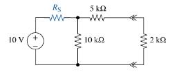
(a) Using Multisim and doing a parameter sweep from \(1 \Omega\). to \(1 \mathrm{M} \Omega\). of \(R_{\mathrm{S}}\) for the circuit of Figure \(\mathrm{P}_{3}-61\), find the value of \(R_{\mathrm{S}}\) that will result in the maximum power delivered to the \(2-\mathrm{k} \Omega\) load.(b) Explain
A 1-k \(\Omega\) load needs \(10 \mathrm{~mA}\) to operate correctly. Design a practical power source to provide the needed current. The smallest source resistance you can practically design for is \(50 \Omega\), but you can add any other series resistance if you need to.
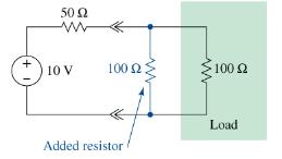
A10-V source is shown in Figure P3–63 that is used to power a 100-Ω load. Clearly, the load does not match the source resistance for maximum power. A young engineer decides to obtain maximum power from the source by adding a 100-Ω shunt resistor across the load. Has he achieved his goal of
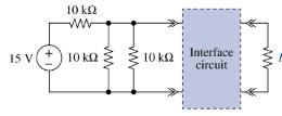
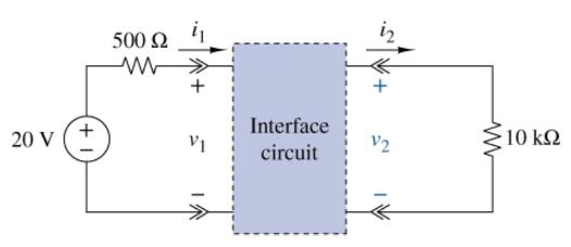
(a) Select \(R_{\mathrm{L}}\) and design an interface circuit for the circuit shown in Figure P \(3=64\) so that the load voltage is 2 \(\mathrm{V}\).(b) Suppose that the load was set at \(15 \mathrm{k} \Omega\). Now design an appropriate interface so that the load voltage is \(2 \mathrm{~V}\). 15
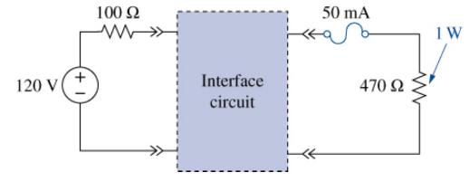
A particular instrument can be modeled as a \(470-\Omega\) resistor. It is protected by a \(50-\mathrm{mA}\) fuse with negligible resistance. It needs \(1 \mathrm{~W}\) to operate correctly. The available source can be modeled as a \(120-\mathrm{V}\) source with a \(100-\Omega\) series resistor as
There is a need to deliver \(5 \mathrm{~V}\) to a 100- \(\Omega\) load. There are two sources available that can satisfy the task as shown in Figure P3-66.(a) Design an appropriate interface for each source. The goal is to minimize the power provided by the source while delivering \(5 \mathrm{~V}\)
Design the interface circuit in Figure P3-67. so that the voltage delivered to the load is \(v=10 \mathrm{~V} \pm 10 \%\). Use one or more of only the following standard resistors: \(1.3 \mathrm{k} \Omega, 2 \mathrm{k} \Omega, 3\) \(\mathrm{k} \Omega, 4.3 \mathrm{k} \Omega, 6.2 \mathrm{k} \Omega\),
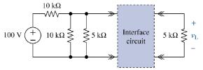
In this problem, you will design two interface circuits that deliver \(15 \mathrm{~V}\) to the \(5-\mathrm{k} \Omega\) load shown in Figure \(\mathrm{P}_{3}=\) 68.(a) Design a series resistor interface to meet the requirement.(b) (D) Convert the source circuit to its Norton equivalent and then
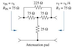
The bridge-T attenuation pad shown in Figure P3 3 -69 was found in a drawer. You need an attenuation pad that would match to a \(75-\Omega\) source and a \(75-\Omega\) load and provide for a - 12-dB drop of signal (reduction of four times). Use Multisim to determine if the device will work. VIN =
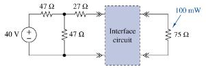
Design two interface circuits in Figure P3=70 so that the power delivered to the load is \(100 \mathrm{~mW}\). In one case use a series interface resistor, and in the second case use a parallel resistor to attain the same result. Evaluate your interface circuits and determine which one results in
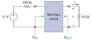
Design the interface circuit in Figure P \(3=71\) so that \(R_{\text {IN }}=100 \Omega\) and the current delivered to the \(50-\Omega\) load is \(i\) \(=50 \mathrm{~mA}\). 15 V + 100 (2 RIN Interface circuit ROUT 5002
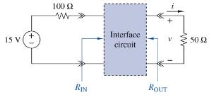
Design the interface circuit in Figure P3=71 so that \(R\) OUT \(=50 \Omega\) and the voltage delivered to the \(50-\Omega\) load is \(v=\) 2.5V. 15 V + 100 (2 Ww RIN Interface. circuit ROUT 50 22
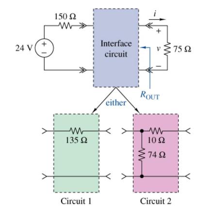
It is claimed that both interface circuits in Figure \(\underline{P}_{3}=7.3\) will deliver \(v=5 \mathrm{~V}\) to the \(75-\Omega\) load. Verify this claim. Which interface circuit consumes the least power? Which has an output resistance that best matches the \(75-\Omega\) load? 24 V | 150 135
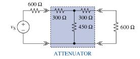
In Figure P3=74, a two-port attenuator connects a \(600-\Omega\) source to a \(600-\Omega\) load. Find the power delivered to the load in terms of \(v_{\mathrm{S}}\). Remove the attenuator and find the power delivered to the load when the source is directly connected to the load. By what fraction
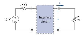
Using no more than three \(75-\Omega\) resistors, design the interface circuit in Figure P \(3=76\) so that \(v \leq 4 \mathrm{~V}\) and \(i \leq 50 \mathrm{~mA}\) regardless of the value of \(R_{\mathrm{L}}\). 12 V 7592 ww Interface circuit
A satellite requires a battery with an open-circuit voltage \(v_{\mathrm{OC}}=\) \(36 \mathrm{~V}\) and a Thévenin resistance \(R_{\mathrm{T}} \leq 102\). The battery is to be constructed using series and parallel combinations of one of two types of cells. The first type has \(v_{\mathrm{OC}}=9
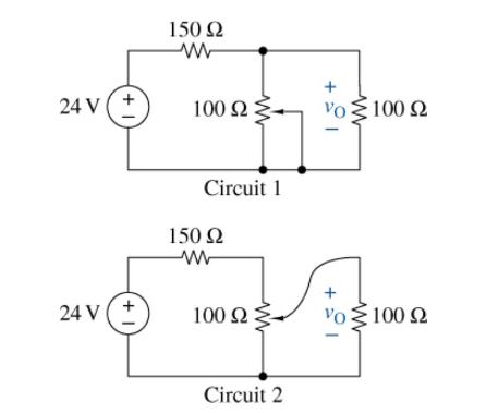
A requirement exists for a circuit to deliver o to \(6 \mathrm{~V}\) to a \(100-\Omega\) load from a \(24-\mathrm{V}\) source rated at \(3.0 \mathrm{~W}\). Two proposed circuits are shown in Figure P \(_{3}=7 \underline{8}\). Which one would you choose and why? +1 24V(+ 24V(+ 150 100 Circuit 1
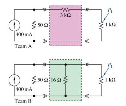
The output of a transistorized power supply is modeled by the Norton equivalent circuit shown in Figure P3=79. Two teams are competing to design the interface circuit so that \(25 \mathrm{~mW} \pm\) \(10 \%\) is delivered to the \(1-\mathrm{k} \Omega\) load resistor. Their designs are shown in
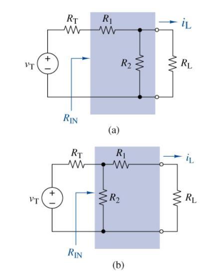
Figure \(\mathrm{P}_{3}-80\) displays two generalized interface circuit designs. In both circuits, resistors \(R_{1}\) and \(R_{2}\) connect a Thévenin equivalent circuit to a load resistor. Using MATLAB, develop symbolic expressions for the load current, \(i_{\mathrm{L}}\), and the input
Figure P3-81 shows a circuit with two sources, a fixed load and a resistor \(R\). Select \(R\) for minimum power transfer to the load. Simulate in Multisim using the "Parameter sweep" under "Analyses" and do a linear sweep for \(R\) from 102 to \(1 \mathrm{M} 2\). Plot the power transferred to the
A noninverting summer interface device is shown in Figure \(\mathrm{P}_{3}=\) 82. Of importance is that the input to the device has infinite resistance-that is, no current flows into the device. The output voltage for this configuration is two times the input voltage. Develop a relationship for the
Figure P \(_{3}-83\) shows a two-way splitter. It takes the input \(V_{\text {IN }}\) and splits it in half delivering it to outputs 1 and 2. The input source resistance and each of the output resistances are \(75 \Omega\). Design the splitter so that each output sees \(75 \Omega\) and the input
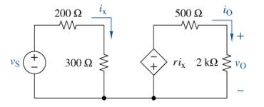
Find the voltage gain \(v_{\mathrm{O}} / v_{\mathrm{S}}\) and current gain \(i_{\mathrm{O}} / i_{\mathrm{X}}\) in Figure P4-1 for \(r=20 \mathrm{k} \Omega\). + 200 300 +1 500 io + rix 2k vo
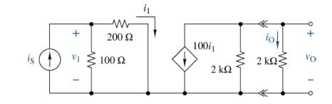
Find the voltage gain \(v_{\mathrm{O}} / v_{1}\) and the current gain \(i_{\mathrm{O}} / i_{\mathrm{S}}\) in Figure P4-2 . For \(i_{\mathrm{S}}=10 \mathrm{~mA}\), find the power supplied by the input current source and the power delivered to the \(2-k \Omega\) output resistor. is ( + 200 100
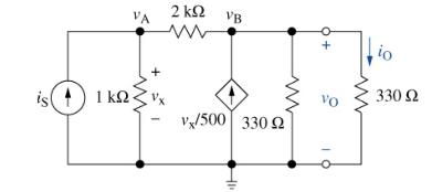
For the circuit in Figure P4=3 :(a) Formulate node-voltage equations, do not solve them.(b) Perform a source transformation on the input and dependent-source circuits and then formulate a meshcurrent analysis of the modified circuit, but do not solve.(c) Use whichever approach is simplest and solve
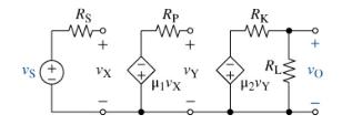
Find the voltage gain \(v_{\mathrm{O}} / v_{\mathrm{S}}\) in Figure \(\mathrm{P}_{4}-4\). R$ www VX 10 Rp ww Vy H1Vx RK www RL HVY VO | 0
(a) Find an expression for the current gain \(i_{\mathrm{O}} / i_{\mathrm{S}}\) in Figure P4=5 (a).(b) Find an expression for the current gain \(i_{\mathrm{O}} / i_{\mathrm{S}}\) in Figure \(\underline{P}_{4}=5\) (b).(c) Simulate both circuits in Multisim. Note: Both of these circuits emulate
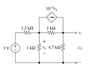
(a) Find the voltage \(v_{\mathrm{O}}\) in Figure P4-6.(b) Validate your answer by simulating the circuit in Multisim. 3V 1.2 10-vx 1 + . 4.7 o+ VO
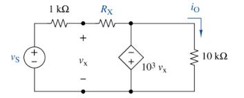
(a) Find an expression for the gain \(i_{\mathrm{O}} / v_{\mathrm{S}}\) Figure \(\mathrm{P}_{4}=7\) in terms of \(R_{\mathrm{X}}\).(b) Select a value for \(R_{\mathrm{X}}\) so that the gain is -0.002 .(c) Simulate the circuit in Multisim and perform a parameter sweep on \(R_{\mathrm{X}}\) from \(10
(a) Find an expression for the voltage gain \(v_{\mathrm{O}} / v_{\mathrm{S}}\) in Figure P4-8.(b) Let \(R_{\mathrm{S}}=1 \mathrm{k} \Omega, R_{\mathrm{L}}=100 \Omega\) and \(\mu=50\). Find the voltage gain \(v_{\mathrm{O}} / v_{\mathrm{S}}\) as a function of \(R_{\mathrm{F}}\). What is the voltage
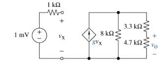
Consider the dependent source circuit of Figure P4=9.(a) Find a relationship between the transconductance gg and the output vOvO.(b) Use this relationship to find the value of gg that would give vO=1 V,5 VvO=1 V,5 V, and 10 V10 V.(c) Validate your answers using Multisim. Use the parameter
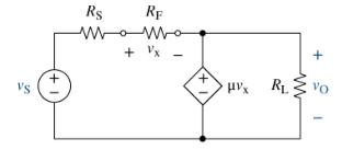
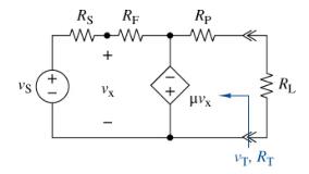
Find the Thévenin equivalent circuit that the load \(R_{\mathrm{L}}\) sees in Figure P4-10 . Repeat the problem with \(R_{\mathrm{F}}\) replaced by an open circuit. VS Rs www + Vx RE + D Rp www HVx ww VT. RT R
For the circuit in Figure P4-11:(a) Find the Thévenin equivalent circuit that the load \(R_{\mathrm{L}}\) sees.(b) Then if \(R_{\mathrm{P}}=R_{\mathrm{S}}=R_{\mathrm{L}}=200 \Omega, r=5 \mathrm{k} \Omega\), and \(v_{\mathrm{S}}=2 \mathrm{~V}\), find the power delivered to the load resistor. VS 1 +
You are a teaching assistant and you administered a quiz for your instructor. The quiz asked the students to find the input resistance to the circuit in Figure P4-12. One of your students said the answer is trivial. No input means that the dependent source was off, and since it is a current source,
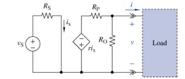
Find the Norton equivalent circuit seen by the load in Figure P4-13 . R$ w + Rp w Ro rix V Load
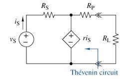
Find the Thévenin equivalent circuit seen by the load in Figure P4-14. is R www 1 Ro ww Load
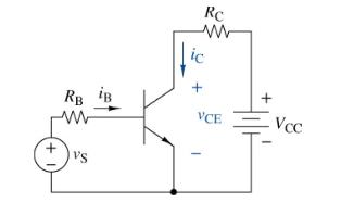
The circuit parameters in Figure \(\mathrm{P}_{4}-15\) are \(R_{\mathrm{B}}=90\) \(\mathrm{k} \Omega, R_{\mathrm{C}}=3.3 \mathrm{k} \Omega, \beta=110, V_{\gamma}=0.7 \mathrm{~V}\), and \(V_{\mathrm{CC}}=15 \mathrm{~V}\). Find \(i_{\mathrm{C}}\)and \(v_{\mathrm{CE}}\) for \(v_{\mathrm{S}}=0.5
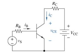
The circuit parameters in Figure P4-15 are \(R_{C}=2\) \(\mathrm{k} \Omega, \beta=90, V_{\gamma}=0.7 \mathrm{~V}\), and \(V_{\mathrm{CC}}=5 \mathrm{~V}\). Select a value of \(R_{\mathrm{B}}\) such that the transistor is in the saturation mode when \(v_{\mathrm{S}} \geq 2 \mathrm{~V}\). RB VS Rc www
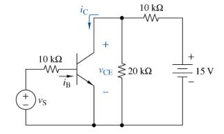
The parameters of the transistor in Figure P4-17 are \(\beta=100\) and \(V_{\mathrm{Y}}=0.7 \mathrm{~V}\). Find \(i_{\mathrm{C}}\) and \(v_{\mathrm{CE}}\) for \(v_{\mathrm{S}}=0.8 \mathrm{~V}\). Repeat for \(v_{\mathrm{S}}=2.5 \mathrm{~V}\). +1 10 VS + 10 VCH 20 + 15 V
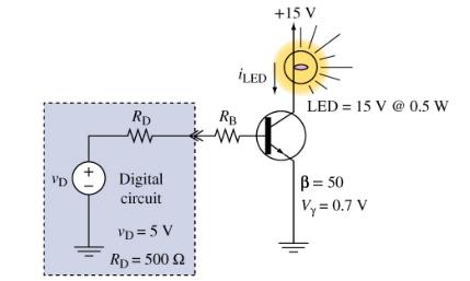
An emergency indicator light uses a bright \(15 \mathrm{~V} @ 0.5 \mathrm{~W}\) LED indicator. It is to be ON when a digital output is high (5 V). The digital circuit does not have sufficient power to turn on the LED directly. However, as is common practice, a transistordriver is used as a digital
Showing 4200 - 4300
of 5433
First
36
37
38
39
40
41
42
43
44
45
46
47
48
49
50
Last
Step by Step Answers