New Semester
Started
Get
50% OFF
Study Help!
--h --m --s
Claim Now
Question Answers
Textbooks
Find textbooks, questions and answers
Oops, something went wrong!
Change your search query and then try again
S
Books
FREE
Study Help
Expert Questions
Accounting
General Management
Mathematics
Finance
Organizational Behaviour
Law
Physics
Operating System
Management Leadership
Sociology
Programming
Marketing
Database
Computer Network
Economics
Textbooks Solutions
Accounting
Managerial Accounting
Management Leadership
Cost Accounting
Statistics
Business Law
Corporate Finance
Finance
Economics
Auditing
Tutors
Online Tutors
Find a Tutor
Hire a Tutor
Become a Tutor
AI Tutor
AI Study Planner
NEW
Sell Books
Search
Search
Sign In
Register
study help
computer science
introduction java program
Fundamentals Of Digital Logic With Verilog Design 3rd Edition Stephen Brown, Zvonko Vranesic - Solutions
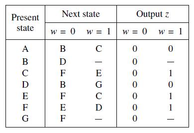
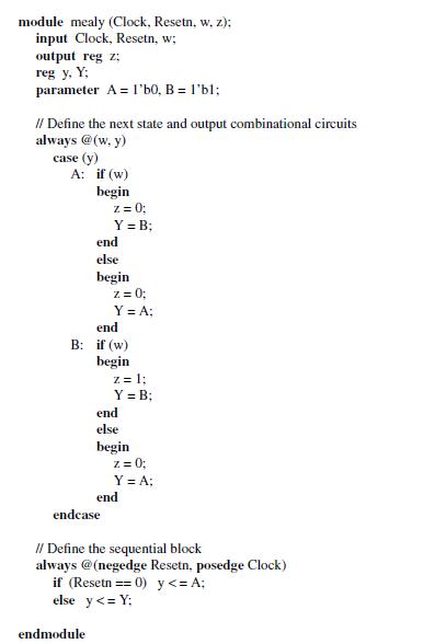
In Figure 6.59 assume that the unspecified outputs in states B andG are 1 and 0, respectively. Derive the minimized state table for this FSM. Present state A B C D E F G Next state Output z w = 0 w = 1 w = 0 w = 1 0 B D F B F E F CEGCAI с с D 0 0 0 0 0 0 0 1 0 1 1
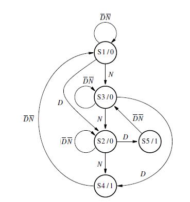
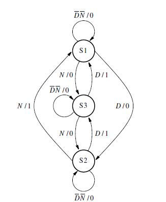
Derive circuits that implement the FSMs defined in Figures 6.57 and 6.58. Can you draw any conclusions about the complexity of circuits that implement Moore and Mealy types of machines? DN DN DN D DN S1/0) S3/0 N N $2/0 N S4/1 DN S5/1 D
Design a counter that counts pulses on line w and displays the count in the sequence 0, 2, 1, 3, 0, 2, . . . . Use D flip-flops in your circuit.
Repeat Problem 6.20 using JK flip-flops.Data From Problem 6.20.Design a counter that counts pulses on line w and displays the count in the sequence 0, 2, 1, 3, 0, 2, . . . . Use D flip-flops in your circuit.
Repeat Problem 6.20 using T flip-flops.Data From Problem 6.20.Design a counter that counts pulses on line w and displays the count in the sequence 0, 2, 1, 3, 0, 2, . . . . Use D flip-flops in your circuit.
Design a modulo-6 counter, which counts in the sequence 0, 1, 2, 3, 4, 5, 0, 1, . . . . The counter counts the clock pulses if its enable input, w, is equal to 1. Use D flip-flops in your circuit.
Repeat Problem 6.23 using JK flip-flops.Data From Problem 6.23Design a modulo-6 counter, which counts in the sequence 0, 1, 2, 3, 4, 5, 0, 1, . . . . The counter counts the clock pulses if its enable input, w, is equal to 1. Use D flip-flops in your circuit.
Repeat Problem 6.23 using T flip-flops.Data From Problem 6.23Design a modulo-6 counter, which counts in the sequence 0, 1, 2, 3, 4, 5, 0, 1, . . . . The counter counts the clock pulses if its enable input, w, is equal to 1. Use D flip-flops in your circuit.
Design a three-bit counterlike circuit controlled by the input w. If w = 1, then the counter adds 2 to its contents, wrapping around if the count reaches 8 or 9. Thus if the present state is 8 or 9, then the next state becomes 0 or 1, respectively. If w = 0, then the counter subtracts 1 from its
Repeat Problem 6.26 using JK flip-flops.Data From Problem 6.26Design a three-bit counterlike circuit controlled by the input w. If w = 1, then the counter adds 2 to its contents, wrapping around if the count reaches 8 or 9. Thus if the present state is 8 or 9, then the next state becomes 0 or 1,
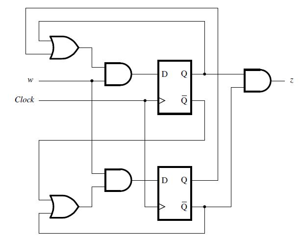
Derive the state table for the circuit in Figure P6.2. What sequence of input values on wire w is detected by this circuit? W Clock D D Q DPT Q D Z
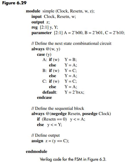
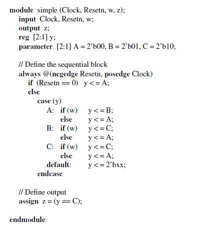
Repeat Problem 6.30, using the style of code in Figure 6.34.Data From Problem 6.30Write Verilog code for the FSM shown in Figure 6.57, using the style of code in Figure 6.29. module simple (Clock, Resetn, w, z); input Clock, Resetn, w; output z; reg [2:1] y; parameter [2:1] A = 2'600, B = 2'b01, C
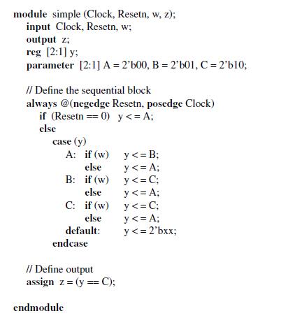
Write Verilog code for the FSM shown in Figure 6.57, using the style of code in Figure 6.29. DN D DN DN D DN S1/0 $3/0 N N ($2/0) N $4/1 DN S5/1
Repeat Problem 6.26 using T flip-flops.Data From Problem 6.26Design a three-bit counterlike circuit controlled by the input w. If w = 1, then the counter adds 2 to its contents, wrapping around if the count reaches 8 or 9. Thus if the present state is 8 or 9, then the next state becomes 0 or 1,
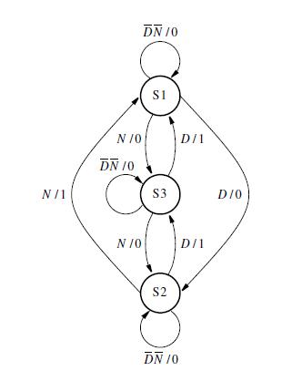
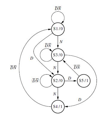
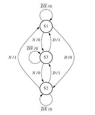
Write Verilog code for the FSM shown in Figure 6.58, using the style of code in Figure 6.29. N/1 DE N/0 DN 10 DN 10 N/0 S1 S3 S2 DN 10 D/1 D/1 D/O
Repeat Problem 6.32, using the style of code in Figure 6.34.Data From Problem 6.32 WriteVerilog code for the FSM shown in Figure 6.58, using the style of code in Figure 6.29. module simple (Clock, Resetn, w, z); input Clock, Resetn, w; output z; reg [2:1] y; parameter [2:1] A = 2'600, B =
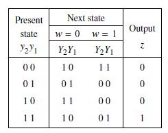
Write Verilog code for the FSM shown in Figure P6.1. Present state Y2Y1 00 01 10 11 Next state w = 0 Y2Y1 10 01 11 10 w = 1 Y2Y1 00 00 01 Output N 0 0 0 1
Represent the FSM in Figure 6.57 in form of an ASM chart. DN D DN DN D DN S1/0 $3/0 N N ($2/0) N S4/1 DN S5/1
Represent the FSM in Figure 6.58 in form of an ASM chart. N/1 N/0 DN 10 DN/0 N 10 S1 S3 S2 DN 10 D/1 D/1 D/0
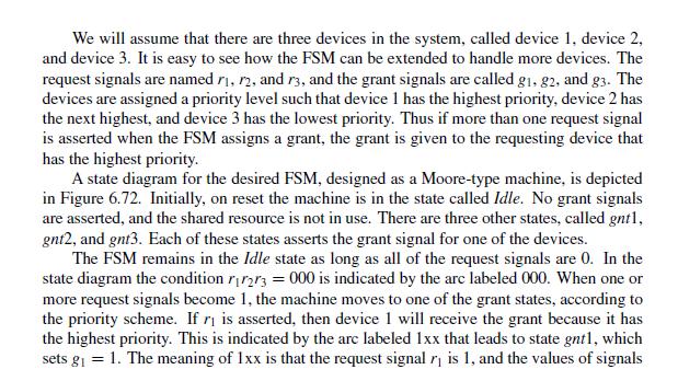
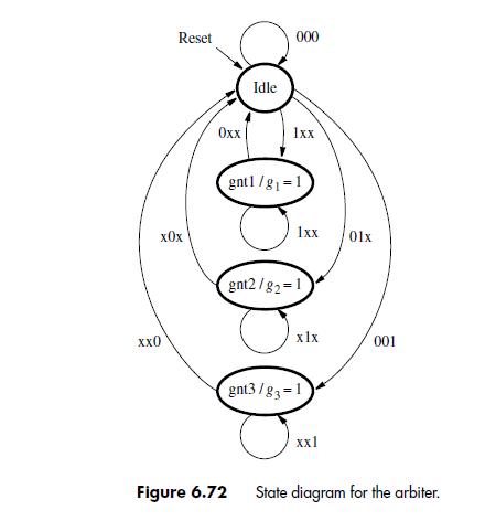
The arbiter FSM defined in Section 6.8 (Figure 6.72) may cause device 3 to never get serviced if devices 1 and 2 continuously keep raising requests, so that in the Idle state it always happens that either device 1 or device 2 has an outstanding request. Modify the proposed FSM to ensure that device
Write Verilog code for the FSM designed in Problem 6.37.Data From Problem 6.37The arbiter FSM defined in Section 6.8 (Figure 6.72) may cause device 3 to never get serviced if devices 1 and 2 continuously keep raising requests, so that in the Idle state it always happens that either device 1 or
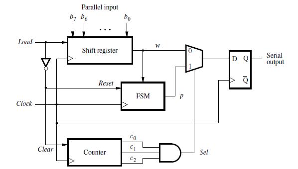
Write Verilog code to specify the circuit in Figure 6.97. Load Clock Clear Parallel input by b6 ... Shift register Reset Counter bo CO FSM W Sel DQ 10 Serial output
Section 6.5 presents a design for the serial adder. Derive a similar circuit that functions as a serial subtractor which produces the difference of operands A and B.Data From Section 6.5We will now present another simple example that illustrates the complete design process. In Chapter 3 we
In Section 6.2 we stated that trying all possible state assignments in order to find the best one is impractical. Determine the number of possible state assignments for an FSM that has n states and for which k = log2n state variables are used. Data From Section 6.2 Having introduced the basic
Write Verilog code that defines the serial subtractor designed in Problem 6.40.Data From Problem 6.40Section 6.5 presents a design for the serial adder. Derive a similar circuit that functions as a serial subtractor which produces the difference of operands A and B.Data From Section 6.5Serial Adder
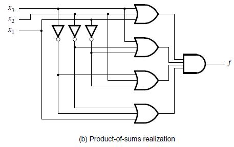
Repeat Problem 2.60 for the circuit in Figure 2.32b.Data From Problem 2.60Write Verilog code to implement the circuit in Figure 2.32a using the gate level primitives. 好 上 前 如 D D (b) Product-of-sums realization
Write Verilog code to implement the function f (x1, x2, x3) = Σm(0, 1, 3, 4, 5, 6) using the continuous assignment.
(a) Write Verilog code to describe the following functionsf1 = x1x3 + x2x3 + x3x4 + x1x2 + x1x4f2 = (x1 + x3) · (x1 + x2 + x4) · (x2 + x3 + x4)(b) Use functional simulation to prove that f1 = f2.
Show how the function f (w1, w2, w3) = Σm(0, 2, 3, 4, 5, 7) can be implemented using a 3-to-8 binary decoder and an OR gate.
Show how the function f (w1, w2, w3) = Σm(1, 2, 3, 5, 6) can be implemented using a 3-to-8 binary decoder and an OR gate.
Consider the function f = w1w3 + w2w3 + w1w2. Use the truth table to derive a circuit for f that uses a 2-to-1 multiplexer.
Repeat Problem 4.3 for the function f = w2w3 + w1w2.Data From Problem 4.3Consider the function f = w1w3 + w2w3 + w1w2. Use the truth table to derive a circuit for f that uses a 2-to-1 multiplexer.
For the function f (w1, w2, w3) = Σm(0, 2, 3, 6), use Shannon’s expansion to derive an implementation using a 2-to-1 multiplexer and any other necessary gates.
Write Verilog code that represents the function in Problem 4.2, using a case statement.Data From Problem 4.2Show how the function f (w1, w2, w3) = Σm(1, 2, 3, 5, 6) can be implemented using a 3-to-8 binary decoder and an OR gate.
Repeat Problem 4.5 for the function f (w1, w2, w3) = Σm(0, 4, 6, 7).Data From Problem 4.5For the function f (w1, w2, w3) = Σm(0, 2, 3, 6), use Shannon’s expansion to derive an implementation using a 2-to-1 multiplexer and any other necessary gates.
Consider the function f = w2 + w1w3 + w1w3. Show how repeated application of Shannon’s expansion can be used to derive the minterms off.
Repeat Problem 4.7 for f = w2 + w1w3.Data From Problem 4.7Consider the function f = w2 + w1w3 + w1w3. Show how repeated application of Shannon’s expansion can be used to derive the minterms off.
Prove Shannon’s expansion theorem presented in Section 4.1.2.Section 4.1.2Figures 4.6 through 4.9 illustrate how truth tables can be interpreted to implement logic functions using multiplexers. In each case the inputs to the multiplexers are the constants 0 and 1, or some variable or its
Section 4.1.2 shows Shannon’s expansion in sum-of-products form. Using the principle of duality, derive the equivalent expression in product-of-sums form.Section 4.1.2Figures 4.6 through 4.9 illustrate how truth tables can be interpreted to implement logic functions using multiplexers. In
Consider the function f = w1w2 + w2w3 + w1w2w3. The cost of this minimal sum-of products expression is 14, which includes four gates and 10 inputs to the gates. Use Shannon’s expansion to derive a multilevel circuit that has a lower cost and give the cost of your circuit.
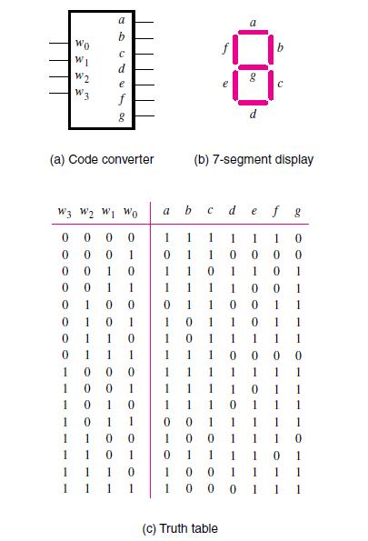
Derive minimal sum-of-products expressions for the outputs a, b, and c of the 7-segment display in Figure 4.21. 0 0 Wo WI 0 W2 W3 0 a b (a) Code converter C W3 W2 WI WO 0 0 00 0 0 0 1 0 1 1 1 01 0 1 1 0 0 1 1 1 10 00 1 0 0 1 10 10 10 11 11 1 1 11 1 1 f 8 0 1 0 1 0 0 00 01 10 a b 1 1 1 01 1
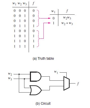
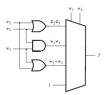
For the function, f , in Example 4.26 perform Shannon’s expansion with respect to variables w1 and w2, rather than w1 and w4. How does the resulting circuit compare with the circuit in Figure 4.46? W2 W5 W3 D W₂W5 W3W5 W2+W3 W₁ W4 - f
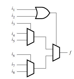
Consider the multiplexer-based circuit illustrated in Figure P4.1. Show how the function f = w2w3 + w1w3 + w2w3 can be implemented using only one instance of this circuit. in in iz i4 is in ig 슈 슈 f
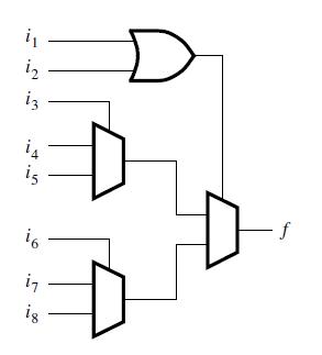
Show how the function f = w1w3 + w1w3 + w2w3 + w1w2 can be realized using one or more instances of the circuit in Figure P4.1. in in is i4 is 16 in ig 수 슈
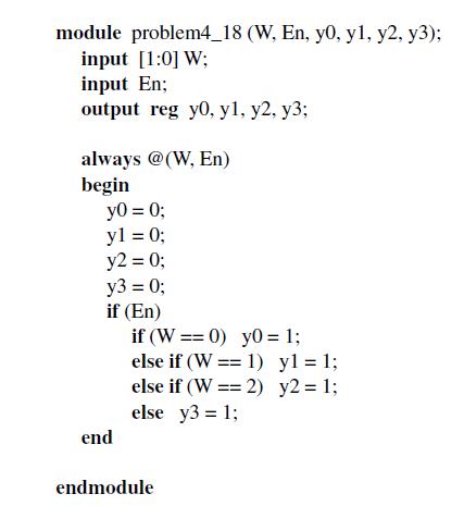
Consider the Verilog code in Figure P4.2. What type of circuit does the code represent? Comment on whether or not the style of code used is a good choice for the circuit that it represents. module problem4_18 (W, En, y0, y1, y2, y3); input [1:0] W; input En; output reg y0, y1, y2, y3; always @(W,
Write Verilog code for a 4-to-2 binary encoder.
Repeat Problem 4.24, using a for loop.Data From Problem 4.24Using a casex statement, write Verilog code for an 8-to-3 priority encoder.
Using a casex statement, write Verilog code for an 8-to-3 priority encoder.
Derive the circuit for an 8-to-3 priority encoder.
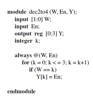
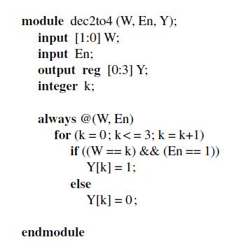
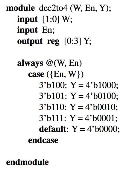
Figure P4.3 shows a modified version of the code for a 2-to-4 decoder in Figure 4.37. This code is almost correct but contains one error. What is the error? module dec2t04 (W, En, Y); input [1:0] W; input En; output reg [0:3] Y; integer k; always @(W, En) for (k = 0; k
Write Verilog code for an 8-to-3 binary encoder.
Create a Verilog module named if 2 to 4 that represents a 2-to-4 binary decoder using an if-else statement. Create a second module named h 3 to 8 that represents the 3-to-8 binary decoder in Figure 4.15 using two instances of the if2to4 module.
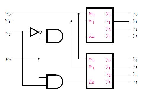
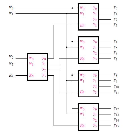
Create a Verilog module named h6to64 that represents a 6-to-64 binary decoder. Use the treelike structure in Figure 4.16, in which the 6-to-64 decoder is built using nine instances of the h3to8 decoder created in Problem 4.26.Data From Problem 4.26Create a Verilog module named if2to4 that
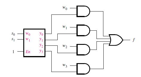
Write Verilog code that represents the circuit in Figure 4.17. Use the dec2to4 module in Figure 4.31 as a subcircuit in your code. So $1 - WO W₁ En Yo y Y₁ V₂ V3 Wo W1 W2 W3 D D D D f
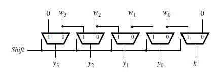
Design a shifter circuit, similar to the one in Figure 4.50, which can shift a four-bit input vector, W = w3w2w1w0, one bit-position to the right when the control signal Right is equal to 1, and one bit-position to the left when the control signal Left is equal to 1. When Right = Left = 0, the
Design a circuit that can multiply an eight-bit number, A = a7, . . . , a0, by 1, 2, 3 or 4 to produce the result A, 2A, 3A or 4A, respectively.
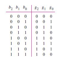
Figure 4.47 depicts the relationship between the binary and Gray codes. Design a circuit that can convert Gray code into binary code. b₂ b₁ b₁ bo 000 0 0 1 010 0 1 1 100 101 110 1 1 1 82 81 80 0 00 00 1 01 1 01 0 11 0 11 1 01 00 10 10
Write Verilog code that implements the task in Problem 4.30.Data From Problem 4.30Design a circuit that can multiply an eight-bit number, A = a7, . . . , a0, by 1, 2, 3 or 4 to produce the result A, 2A, 3A or 4A, respectively.
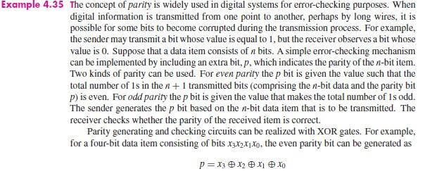
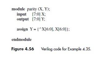
Example 4.35 and Figure 4.56 show how a circuit that generates an ASCII byte suitable for sending over a communications link may be defined. Write Verilog code for its counterpart at the receiving end, where byte Y (which includes the parity bit) has to be converted into byte X in which the bit x7
(a) Show the location of all minterms in a three-variable Venn diagram.(b) Show a separate Venn diagram for each product term in the function f = x1x2x3 + x1x2 + x1x3. Use the Venn diagram to find the minimal sum-of-products form of f.
Repeat Problem 2.37 for the function f (x1, . . . , x5) = Σm(1, 4, 6, 7, 9, 10, 12, 15, 17, 19, 20, 23, 25, 26, 27, 28, 30, 31) + D(8, 16, 21, 22).Data From Problem 2.37Find the minimum-cost SOP and POS forms for the function f (x1, x2, x3) = Σm(1, 2, 3, 5).
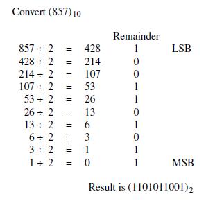
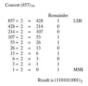
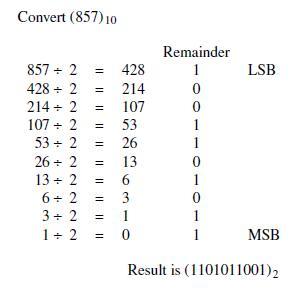
Convert the following decimal numbers into binary, using the method shown in Figure 1.6.(a) (20)10(b) (100)10(c) (129)10(d) (260)10(e) (10240)10 Convert (857) 10 857 + 2 = 428 2 214 - 2 107 + 2 53 2 26 + 2 13 + 2 6+ 2 3+2 1 +
Repeat Problem 3 using the method described in Problem 4.Problem 3Convert the following decimal numbers into binary, using the method shown in Figure 1.6.(a) (1000)10(b) (10000)10(c) (100000)10(c) (1000000)10 Convert (857) 10 857 + 2 = 428 2 214 + 2 107 + 2 53 ÷ 2 26 + 2 13 + 2 6+ 2 3+2 1 +
Convert the following decimal numbers into binary, using the method shown in Figure 1.6.(a) (30)10(b) (110)10(c) (259)10(d) (500)10(e) (20480)10 Convert (857) 10 857 + 2 = 428 2 214 + 2 107 + 2 53 ÷ 2 26 + 2 13 + 2 6+ 2 3+2 1 +
Convert the following decimal numbers into binary, using the method shown in Figure 1.6.(a) (1000)10(b) (10000)10(c) (100000)10(c) (1000000)10 Convert (857) 10 857 + 2 = 428 2 214 + 2 107 + 2 53 ÷ 2 26 + 2 13 + 2 6+2 3+2 1 +
In Figure 1.6 we show how to convert a decimal number into binary by successively dividing by 2. Another way to derive the answer is to construct the number by using powers of 2. For example, if we wish to convert the number (23)10, then the largest power of 2 that is not larger than 23 is 24 = 16.
Convert the following binary numbers into decimal.(a) (1001)2(b) (11100)2(c) (111111)2(d) (101010101010)2
Convert the following binary numbers into decimal.(a) (110010)2(b) (1100100)2(c) (11001000)2(d) (110010000)2
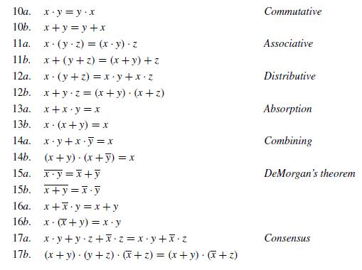
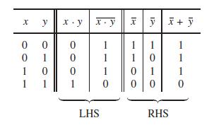
Use the Venn diagram to prove DeMorgan’s theorem, as given in expression 15b in Section 2.5.Section 2.5In 1849 George Boole published a scheme for the algebraic description of processes involved in logical thought and reasoning [1]. Subsequently, this scheme and its further refinements became
What is the minimum number of bits needed to represent the following decimal numbers in binary?(a) (270)10(b) (520)10(c) (780)10(d) (1029)10
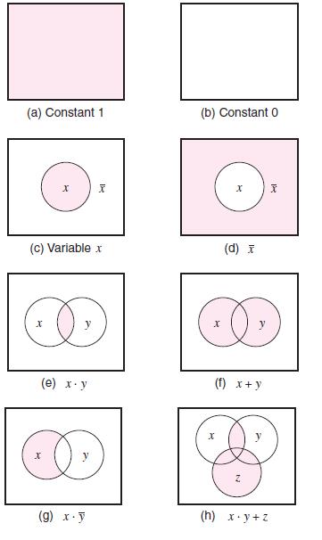
Use the Venn diagram to prove the identity in Problem 2.3.Problem 2.3Use algebraic manipulation to prove that xy + yz + xz = xy + xz. (a) Constant 1 X (c) Variable x A (e) x-y X (g) x.y (b) Constant 0 X X X (d) x (f) x + y A (h) x+y+z 21
Repeat Problem 8 for the following decimal numbers:(a) (111)10(b) (333)10(c) (555)10(d) (1111)10Data From Problem 8What is the minimum number of bits needed to represent the following decimal numbers in binary?(a) (270)10(b) (520)10(c) (780)10(d) (1029)10
Use algebraic manipulation to prove that x + yz = (x + y) · (x + z).
Use algebraic manipulation to prove that (x + y) · (x + y) = x.
Use algebraic manipulation to prove that xy + yz + xz = xy + xz.
Use the Venn diagram to prove that (x₁ + x₂ + x3)(x₁ + x₂ + x3) = x1 + x2
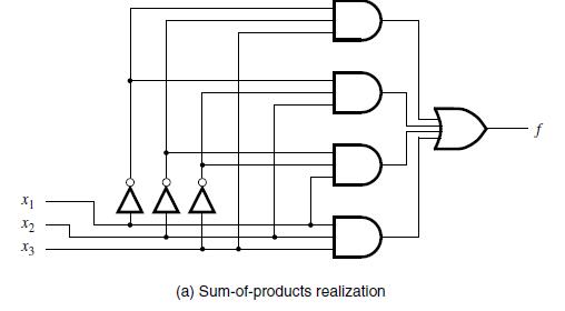
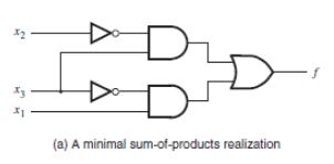
Draw a timing diagram for the circuit in Figure 2.24a. Show the waveforms that can be observed on all wires in the circuit. J2 x3 31 D D (a) A minimal sum-of-products realization
Determine whether or not the following expressions are valid, i.e., whether the left- and right-hand sides represent the same function.(a) x1x3 + x1x2x3 + x1x2 + x1x2 = x2x3 + x1x3 + x2x3 + x1x2x3(b) x1x3 + x2x3 + x2x3 = (x1 + x2 + x3)(x1 +
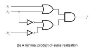
Repeat Problem 2.8 for the circuit in Figure 2.24b.Data From Problem 2.8Draw a timing diagram for the circuit in Figure 2.24a. Show the waveforms that can be observed on all wires in the circuit. Τ Κα 2 ΔΔ D D (b) A minimal product-of-sums realization
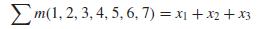
Use algebraic manipulation to show that for three input variables x1, x2, and x3 m(1, 2, 3, 4, 5, 6, 7) = x₁ + x2 + x3
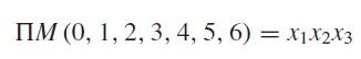
Use algebraic manipulation to show that for three input variables x1, x2, and x3 ΠΜ (0, 1, 2, 3, 4, 5, 6) = X1X2X3
Represent the function in Figure 2.23 in the form of a Venn diagram and find its minimal sum-of-products form. Row number X₁ X₂ x3 0123 67 0 0 0 1 1 0 0 1 1 0 0 00 4 1 5 1 0 0 0 1 1 0 11 1 f(x₁, x₂, x3) 0 1 0 0 1 1 1 0
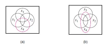
Figure P2.1 shows two attempts to draw a Venn diagram for four variables. For parts (a) And (b) Of the figure, explain why theVenn diagram is not correct. 1x Ex X4 (a) X2 X1 X3 XA (b) X2
Use algebraic manipulation to find the minimum sum-of-products expression for the function f = x1x3 + x1x2 + x1x2x3 + x1x2x3.
Use algebraic manipulation to find the minimum sum-of-products expression for the function f = x1x2x3 + x1x2x4 + x1x2x3x4.
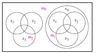
Figure P2.2 gives a representation of a four-variable Venn diagram and shows the location of minterms m0,m1, and m2. Show the location of the other minterms in the diagram. Represent the function f = x1x2x3x4 + x1x2x3x4 + x1x2 on this diagram. X1 Ex X2 m₂ mo X1 m₁ X4 Ex x₂
Use algebraic manipulation to find the minimum product-of-sums expression for the function f = (x1 + x3 + x4) · (x1 + x2 + x3) · (x1 + x2 + x3 + x4).
Use algebraic manipulation to find the minimum product-of-sums expression for the function f = (x1 + x2 + x3) · (x1 + x2 + x3) · (x1 + x2 + x3) · (x1 + x2 + x3).
Design the simplest sum-of-products circuit that implements the function f (x1, x2, x3) = Σm(3, 4, 6, 7).
Design the simplest sum-of-products circuit that implements the function f (x1, x2, x3) = Σm(1, 3, 4, 6, 7).
For the timing diagram in Figure P2.3, synthesize the function f (x1, x2, x3) in the simplest sum-of-products form. X2 X3 f Time
Design the simplest product-of-sums circuit that implements the function f (x1, x2, x3) = ΠM(0, 2, 5).
Design the simplest product-of-sums expression for the function f (x1, x2, x3) ΠM(0,1,5,7).
For the timing diagram in Figure P2.3, synthesize the function f (x1, x2, x3) in the simplest product-of-sums form. X2 X3 f Time
Derive the simplest sum-of-products expression for the function f (x1, x2, x3, x4) = x1x3x4 + x2x3x4 + x1x2x3.
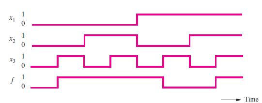
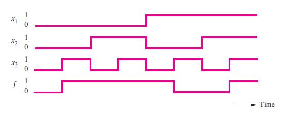
For the timing diagram in Figure P2.4, synthesize the function f (x1, x2, x3) in the simplest product-of-sums form. x2 f Time
Use algebraic manipulation to derive the simplest sum-of-products expression for the function f (x1, x2, x3, x4, x5) = x1x3x5 + x1x3x4 + x1x4x5 + x1x2x3x5.
Use algebraic manipulation to derive the simplest product-of-sums expression for the function f (x1, x2, x3, x4) = (x1 + x3 + x4)(x2 + x3 + x4)(x1 + x2 + x3).
Use algebraic manipulation to derive the simplest product-of-sums expression for the function f (x1, x2, x3, x4, x5) = (x2 + x3 + x5)(x1 + x3 + x5)(x1 + x2 + x5)(x1 + x4 + x5).
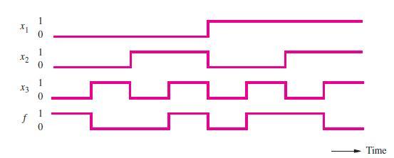
For the timing diagram in Figure P2.4, synthesize the function f (x1, x2, x3) in the simplest sum-of-products form. X2 X3 f 0 0 0 Time
Showing 300 - 400
of 741
1
2
3
4
5
6
7
8
Step by Step Answers