New Semester
Started
Get
50% OFF
Study Help!
--h --m --s
Claim Now
Question Answers
Textbooks
Find textbooks, questions and answers
Oops, something went wrong!
Change your search query and then try again
S
Books
FREE
Study Help
Expert Questions
Accounting
General Management
Mathematics
Finance
Organizational Behaviour
Law
Physics
Operating System
Management Leadership
Sociology
Programming
Marketing
Database
Computer Network
Economics
Textbooks Solutions
Accounting
Managerial Accounting
Management Leadership
Cost Accounting
Statistics
Business Law
Corporate Finance
Finance
Economics
Auditing
Tutors
Online Tutors
Find a Tutor
Hire a Tutor
Become a Tutor
AI Tutor
AI Study Planner
NEW
Sell Books
Search
Search
Sign In
Register
study help
computer science
systems analysis and design 12th
Microelectronics Circuit Analysis And Design 4th Edition Donald A. Neamen - Solutions
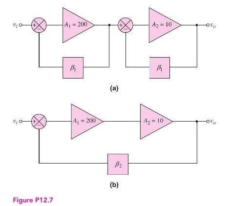
Consider the two feedback networks shown in Figures P12.7(a) and P12.7(b). The \(3 \mathrm{~dB}\) frequency of the amplifier \(A_{1}\) is \(100 \mathrm{~Hz}\) and the \(3 \mathrm{~dB}\) frequency of the second amplifier \(A_{2}\) is very large. The feedback transfer functions are
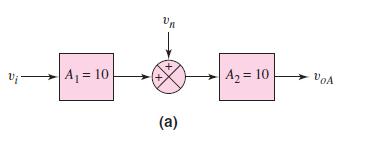
Consider two open-loop amplifiers in cascade, with a noise signal generated between the two amplifiers as in Figure 12.3(a). Assume the amplification of the first stage is \(A_{2}=100\) and that of the second stage is \(A_{1}=1\). If \(V_{\text {in }}=10 \mathrm{mV}\) and \(V_{n}=1 \mathrm{mV}\),
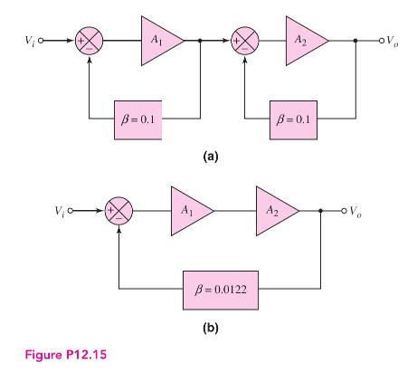
Two feedback configurations are shown in Figures P12.15 (a) and (b). At low input voltages, the two gains are \(A_{1}=A_{2}=90\) and at higher input voltages, the gains change to \(A_{1}=A_{2}=60\). Determine the change in closed-loop gain, \(A_{f}=V_{o} / V_{i}\), for the two feedback circuits.
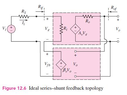
Consider the ideal series-shunt circuit shown in Figure 12.6. Let \(A_{v}=5 \times\) \(10^{3} \mathrm{~V} / \mathrm{V}, \beta=0.0080 \mathrm{~V} / \mathrm{V}, R_{i}=10 \mathrm{k} \Omega\), and \(R_{o}=1 \mathrm{k} \Omega\). Determine the ideal values of \(A_{v f}=V_{o} / V_{i}, R_{i f}\), and
The parameters of the ideal series-shunt circuit shown in Figure 12.6 are \(V_{i}=25 \mathrm{mV}, V_{o}=2.5 \mathrm{~V}\), and \(\beta=0.0096 \mathrm{~V} / \mathrm{V}\). Determine the values and units of \(A_{v}, A_{v f}, V_{f b}\), and \(V_{\varepsilon}\). Vi + Rs ww Rif + VE + Vfb +1 R + Vo BVo
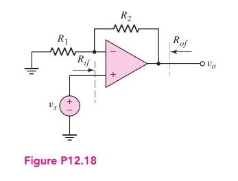
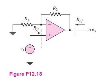
For the noninverting op-amp circuit in Figure P12.18, the parameters are: \(A=10^{5}, A_{v f}=20, R_{i}=100 \mathrm{k} \Omega\), and \(R_{o}=100 \Omega\). Determine the ideal closed-loop input and output resistances, \(R_{i f}\) and \(R_{o f}\), respectively. R www. Rif +1 R www Rof + Figure P12.18
Consider the noninverting op-amp circuit in Figure P12.18. The input resistance of the op-amp is \(R_{i}=\infty\) and the output resistance is \(R_{o}=0\), but the opamp has a finite gain \(A\). (a) Write the closed-loop transfer function in the form\[A_{v f}=\frac{v_{o}}{v_{s}}=\frac{A}{(1+\beta
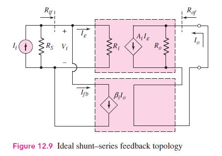
The circuit parameters of the ideal shunt-series amplifier shown in Figure 12.9 are \(I_{i}=20 \mu \mathrm{A}, I_{f b}=19 \mu \mathrm{A}, R_{i}=500 \Omega, R_{o}=20 \mathrm{k} \Omega\), and \(\beta_{i}=\) \(0.0095 \mathrm{~A} / \mathrm{A}\). Determine the values and units of \(I_{\varepsilon},
Consider the ideal shunt-series amplifier shown in Figure 12.9. The parameters are \(I_{i}=25 \mu \mathrm{A}, I_{\varepsilon}=0.8 \mu \mathrm{A}\), and \(A_{i f}=125\). Determine the values and units of \(I_{f b}, I_{o}, \beta_{i}\), and \(A_{i}\). Rif! + Rs Vi T 3 Ifb Bil Ail Ro ww Rof Figure 12.9
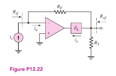
Consider the op-amp circuit in Figure P12.22. The op-amp has a finite gain, so that \(i_{o}=A i_{\varepsilon}\), and a zero output impedance. (a) Write the closed-loop transfer function in the form\[A_{i f}=\frac{i_{o}}{i_{s}}=\frac{A_{i}}{\left(1+\beta_{i} A_{i}\right)}\](b) What is the expression
An op-amp circuit is shown in Figure P12.22. Its parameters are as described in Problem 12.22, except that \(R_{i}=2 \mathrm{k} \Omega\) and \(R_{o}=20 \mathrm{k} \Omega\). Determine the closed-loop input and output resistances, \(R_{i f}\) and \(R_{o f}\), respectively.Data From Problem
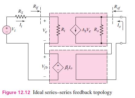
The parameters of the ideal series-series amplifier in Figure 12.12 are \(V_{i}=0.2 \mathrm{mV}, I_{o}=5 \mathrm{~mA}, V_{f b}=0.195 \mathrm{mV}, R_{i}=20 \mathrm{k} \Omega\), and \(R_{o}=10 \mathrm{k} \Omega\). Determine the values and units of \(V_{\varepsilon}, \beta_{z}, A_{g f}, A_{g}, R_{i
The ideal series-series circuit shown in Figure 12.12 has parameters \(V_{i}=150 \mu \mathrm{V}, \beta_{z}=0.0245 \mathrm{~V} / \mathrm{A}\), and \(A_{g}=2000 \mathrm{~A} / \mathrm{V}\). Determine the values and units of \(V_{f b}, V_{\varepsilon}, I_{o}\), and \(A_{g f}\). +1 Rs ww Rif I + Vfb -
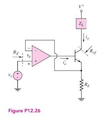
Consider the circuit in Figure P12.26. The input resistance of the op-amp is \(R_{i}=\infty\) and the output resistance is \(R_{o}=0\). The op-amp has a finite gain, so that \(i_{o}^{\prime}=A_{g} v_{\varepsilon}\). The current gain of the transistor is \(h_{F E}\). (a) Write the closed-loop
The circuit shown in Figure P12.26 has the same parameters as described in Problem 12.26, except that \(R_{i}=20 \mathrm{k} \Omega\) and \(R_{o}=50 \mathrm{k} \Omega\). Determine the closed-loop input and output resistances, \(R_{i f}\) and \(R_{o f}\), respectively.Data From Problem
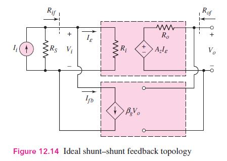
The circuit parameters of the ideal shunt-shunt amplifier shown in Figure 12.14 are \(A_{z f}=0.20 \mathrm{~V} / \mu \mathrm{A}, \beta_{g}=4.25 / \mu \mathrm{A} / \mathrm{V}\), and \(R_{i}=R_{o}=500 \Omega\). Determine the values and units of \(A_{z}, R_{i f}\), and \(R_{o f}\). Rif + Rs Vi R Ifb
Voltage and current values in the ideal shunt-shunt circuit shown in Figure 12.14 are \(I_{i}=40 \mu \mathrm{A}, I_{f b}=38 \mu \mathrm{A}\), and \(V_{o}=8 \mathrm{~V}\). Determine the values and units of \(A_{z}, A_{z f}\), and \(\beta_{g}\). Rif + - I Rs Vi 1fb + - ww Ro R of Als Vo Figure 12.14
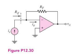
Consider the current-to-voltage converter circuit shown in Figure P12.30. The input resistance \(R_{i f}\) is assumed to be small, the output resistance is \(R_{o}=0\), and the op-amp gain \(A_{z}\) is large. (a) Write the closed-loop transfer function in the form\[A_{z
For the current-to-voltage converter circuit in Figure P12.30, the parameters are as described in Problem 12.30. If \(R_{i}=10 \mathrm{k} \Omega\), determine the closedloop input resistance \(R_{i f}\).Data From Problem 12.30:-Consider the current-to-voltage converter circuit shown in Figure
Determine the type of feedback configuration that should be used in a design to achieve the following objectives: (a) low input resistance and low output resistance, (b) high input resistance and high output resistance, (c) low input resistance and high output resistance, and (d) high input
Consider a series of amplifiers and feedback circuits connected in the ideal feedback configurations. In each case the input resistance to the basic amplifier is \(R_{i}=10 \mathrm{k} \Omega\), the output resistance of the basic amplifier is \(R_{o}=1 \mathrm{k} \Omega\), and the loop gain is
A compound transconductance amplifier is to be designed by connecting two basic feedback amplifiers in cascade. What two amplifiers should be connected in cascade to form the compound circuit? Is there more than one possible design?
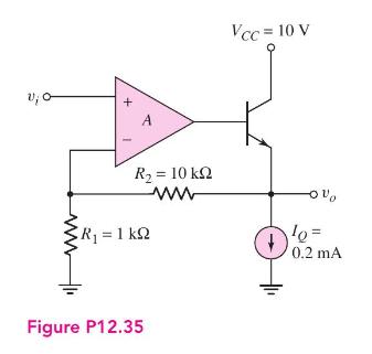
The parameters of the op-amp in the circuit shown in Figure P12.35 are \(A_{v}=10^{5}, R_{i}=30 \mathrm{k} \Omega\), and \(R_{o}=500 \Omega\). The transistor parameters are \(h_{F E}=140\) and \(V_{A}=\infty\). Assume that \(v_{O}=0\) at the quiescent point. Determine (a) \(A_{v f}\), (b) \(R_{i
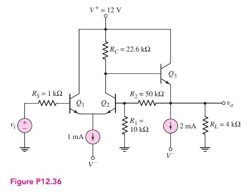
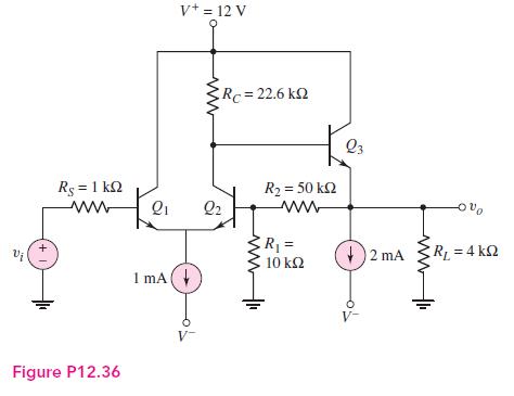
The circuit in Figure P12.36 is an example of a series-shunt feedback circuit. Assume the transistor parameters are: \(h_{F E}=100, V_{B E}(\) on \()=0.7 \mathrm{~V}\), and \(V_{A}=\infty\). (a) Determine the quiescent collector currents and the dc voltage at the output. (b) Determine the
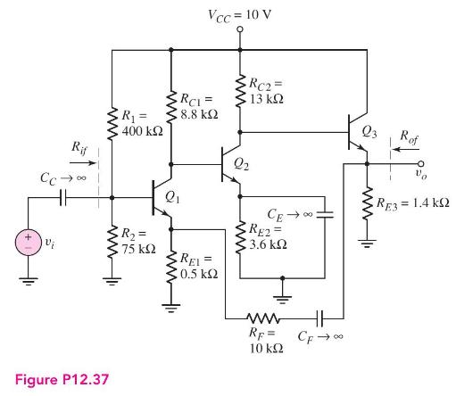
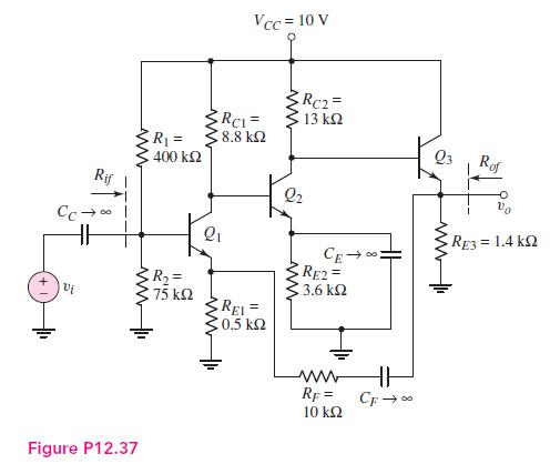
Consider the series-shunt feedback circuit in Figure P12.37, with transistor parameters: \(h_{F E}=120, V_{B E}(\) on \()=0.7 \mathrm{~V}\), and \(V_{A}=\infty\). (a) Determine the small-signal parameters for \(Q_{1}, Q_{2}\), and \(Q_{3}\). Using nodal analysis, determine: (b) the small-signal
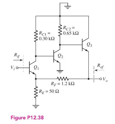
The circuit shown in Figure P12.38 is an ac equivalent circuit of a feedback amplifier. The transistor parameters are \(h_{F E}=100\) and \(V_{A}=\infty\). The quiescent collector currents are \(I_{C 1}=14.3 \mathrm{~mA}, I_{C 2}=4.62 \mathrm{~mA}\), and \(I_{C 3}=\) \(4.47 \mathrm{~mA}\). (a)
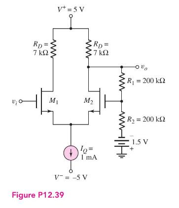
Consider the MOSFET feedback amplifier shown in Figure P12.39. The transistor parameters are \(V_{T N}=0.5 \mathrm{~V}, K_{n}=0.5 \mathrm{~mA} / \mathrm{V}^{2}\), and \(\lambda=0\). Determine the small-signal voltage gain \(A_{v}=v_{o} / v_{i}\). V+= 5 V RD= 7 RD= 7 Mi M2 10= 1 mA R = 200 k2 R =
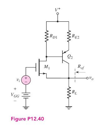
The parameters of the BiCMOS circuit in Figure P12.40 are \(V^{+}=5 \mathrm{~V}\), \(V_{G G}=2.5 \mathrm{~V}, R_{D 1}=5 \mathrm{k} \Omega, R_{E 2}=1.6 \mathrm{k} \Omega\), and \(R_{L}=1.2 \mathrm{k} \Omega\). The transistor parameters are \(K_{n}=1.5 \mathrm{~mA} / \mathrm{V}^{2}, V_{T N}=0.5
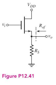
The parameters of the basic source-follower circuit in Figure P12.41 are \(R_{S}=1.5 \mathrm{k} \Omega, V_{T N}=1.2 \mathrm{~V}\), and \(\lambda=0\). Assume the transistor is biased at \(I_{D Q}=1.2 \mathrm{~mA}\). (a) If the transistor conduction parameter is \(K_{n}=\) \(1.5 \mathrm{~mA} /
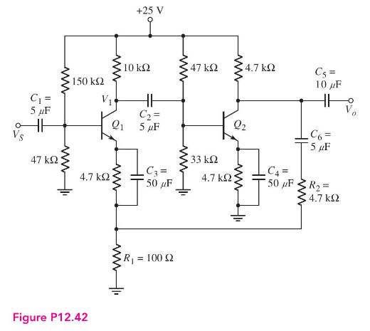
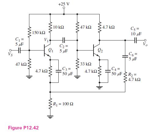
The transistor parameters for the circuit in Figure P12.42 are: \(h_{F E}=50\), \(V_{B E}(\mathrm{on})=0.7 \mathrm{~V}\), and \(V_{A}=\infty\). Using nodal analysis, determine the closedloop small-signal voltage gain \(A_{v f}=v_{o} / v_{s}\) at the midband frequency. C = 5 F www 47 ww 150 www
Design a discrete transistor feedback voltage amplifier to provide a voltage gain of 50. Assume the available transistors have parameters: \(h_{F E}=120\) and \(V_{A}=\infty\). The signal voltage source has a source resistance of \(R_{S}=2 \mathrm{k} \Omega\) and the load is \(R_{L}=3 \mathrm{k}
Redesign the feedback circuit in Figure P12.36 using MOSFETs to provide a voltage gain of \(A_{v f}=8\) and such that \(v_{o}=0\) when \(v_{i}=0\). Assume circuit parameters of \(R_{S}=1 \mathrm{k} \Omega, R_{1}=15 \mathrm{k} \Omega\), and \(R_{L}=10 \mathrm{k} \Omega\). The transistor parameters
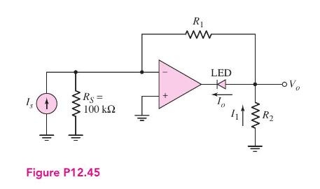
An op-amp current gain amplifier is shown in Figure P12.45. Assuming an ideal op-amp, design the circuit such that the load current is \(I_{o}=5 \mathrm{~mA}\) for an input current of \(I_{s}=60 \mu \mathrm{A}\). Rs = 100 Figure P12.45 R ww LED -OV T R
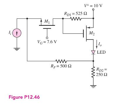
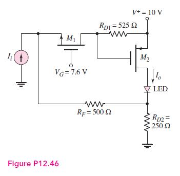
Consider the current gain amplifier shown in Figure P12.46. The transistor parameters are \(K_{n}=K_{p}=10 \mathrm{~mA} / \mathrm{V}^{2}, V_{T N}=1 \mathrm{~V}, V_{T P}=-1 \mathrm{~V}\), and \(\lambda_{n}=\lambda_{p}=0\). The LED turn-on voltage is \(V_{\gamma}=1.6 \mathrm{~V}\). Assume the LED
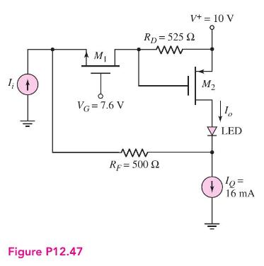
A MOSFET current gain amplifier is shown in Figure P12.47. The transistor parameters are \(K_{n}=K_{p}=10 \mathrm{~mA} / \mathrm{V}^{2}, V_{T N}=1 \mathrm{~V}, V_{T P}=-1 \mathrm{~V}\), and \(\lambda_{n}=\lambda_{p}=0\). The LED turn-on voltage is \(V_{\gamma}=1.6 \mathrm{~V}\). Assume the LED
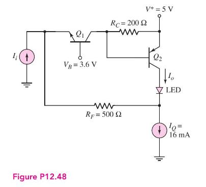
A BJT current gain amplifier is shown in Figure P12.48. The transistor parameters are \(\beta_{1}=\beta_{2}=180, V_{A 1}=V_{A 2}=\infty\), and \(I_{S 1}=I_{S 2}=10^{-15} \mathrm{~A}\). The LED turn-on voltage is \(V_{\gamma}=1.6 \mathrm{~V}\). Assume the LED small-signal resistance is \(r_{f}=0\).
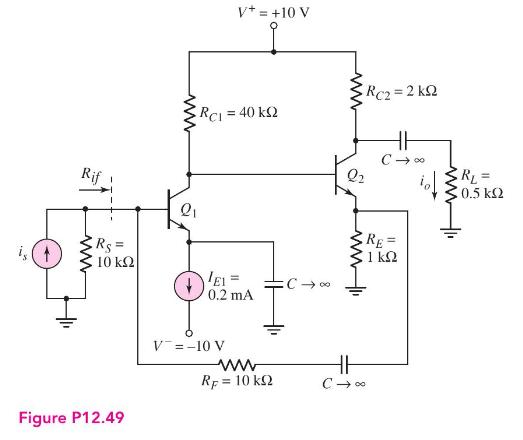
The circuit in Figure P12.49 has transistor parameters: \(h_{F E}=100\), \(V_{B E}(\) on \()=0.7 \mathrm{~V}\), and \(V_{A}=\infty\). (a) From the quiescent values, determine the small-signal parameters for \(Q_{1}\) and \(Q_{2}\). (b) Using nodal analysis, determine the small-signal closed-loop
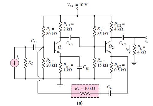
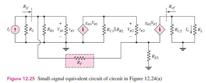
(a) Using the small-signal equivalent circuit in Figure 12.25 for the circuit in Figure 12.24(a), derive the expression for the small-signal current gain \(A_{i f}=I_{o} / I_{s}\). (b) Using the circuit parameters given in Figure 12.24(a) and assuming transistor parameters \(h_{F E}=100\) and
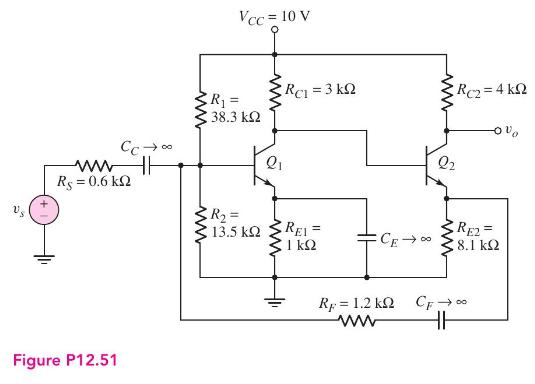
The circuit in Figure P12.51 is an example of a shunt-series feedback circuit. A signal proportional to the output current is fed back to the shunt connection at the base of \(Q_{1}\). However, the circuit may be used as a voltage amplifier. Assume transistor parameters of \(h_{F E}=120, V_{B
Consider the circuit in Figure P12.51 with transistor parameters, \(h_{F E}=120, V_{B E}(\) on \()=0.7 \mathrm{~V}\), and \(V_{A}=\infty\). Using nodal analysis, determine the input resistance \(R_{i f}\). Cc ww Rs = 0.6 k HH Figure P12.51 www www Vcc = 10 V R = 38.3 RC = 3 kQ Rc2=4kQ R = 13.5
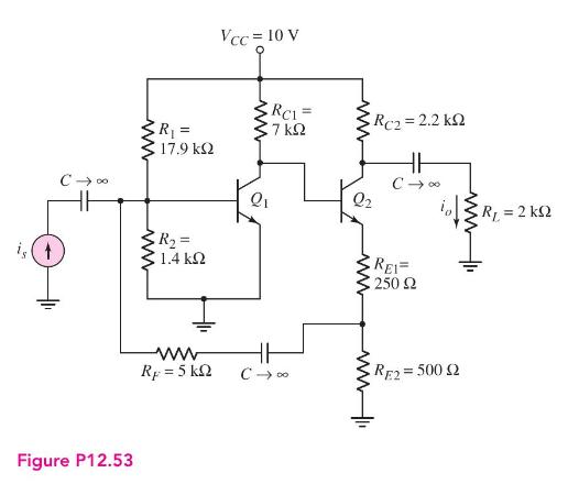
For the transistors in the circuit in Figure P12.53, the parameters are: \(h_{F E}=50, V_{B E}(\) on \()=0.7 \mathrm{~V}\), and \(V_{A}=\infty\). Using nodal analysis, determine the closed-loop current gain \(A_{i f}=i_{o} / i_{s}\). ww Vcc = 10 V R = 17.9 ww RC = 7 Rc2 = 2.2 k R = 1.4 Q www ww
Design a discrete transistor feedback current amplifier to provide a current gain of 30. Assume the available transistors have parameters \(h_{F E}=120\) and \(V_{A}=\infty\). The signal current source has a source resistance of \(R_{S}=25 \mathrm{k} \Omega\) and the load is \(R_{L}=500 \Omega\).
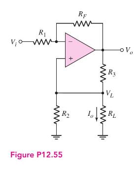
Consider the transconductance amplifier shown in Figure P12.55. Assume the op-amp is ideal. (a) Derive the expression for the transconductance function \(A_{g f}=I_{o} / V_{i}\). (b) If the circuit is designed such that \(R_{F} / R_{1}=\) \(R_{3} / R_{2}\), show that \(I_{o} / V_{i}=-1 / R_{2}\).
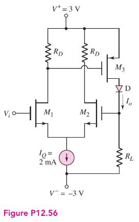
Consider the transconductance feedback amplifier shown in Figure P12.56 with \(R_{D}=1.6 \mathrm{k} \Omega\) and \(R_{L}=248 \Omega\). The transistor parameters are \(V_{T N}=0.5 \mathrm{~V}, V_{T P}=-0.5 \mathrm{~V}, K_{n}=2 \mathrm{~mA} / \mathrm{V}^{2}, K_{p}=10 \mathrm{~mA} / \mathrm{V}^{2}\),
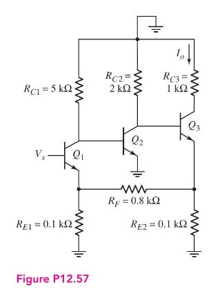
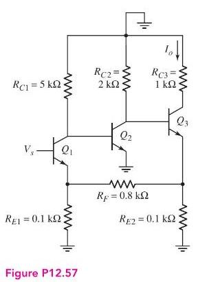
The circuit in Figure P12.57 is the ac equivalent circuit of a series-series feedback amplifier. Assume that the bias circuit, which is not shown, results in quiescent collector currents of \(I_{C 1}=0.5 \mathrm{~mA}, I_{C 2}=1 \mathrm{~mA}\), and \(I_{C 3}=\) \(2 \mathrm{~mA}\). Assume transistor
Using a computer simulation analysis, redesign the circuit in Figure P12.57 by changing the value of \(R_{F}\) to achieve a transconductance gain of \(A_{g f}=\) \(I_{o} / V_{s}=120 \mathrm{~mA} / \mathrm{V}\). Rc1 = 5kQ ww Rc2=1 2 Rc3=1 1 V- Q2 Q3 REI 0.1 KQ2 Figure P12.57 www Rp = 0.8 k RE2 =
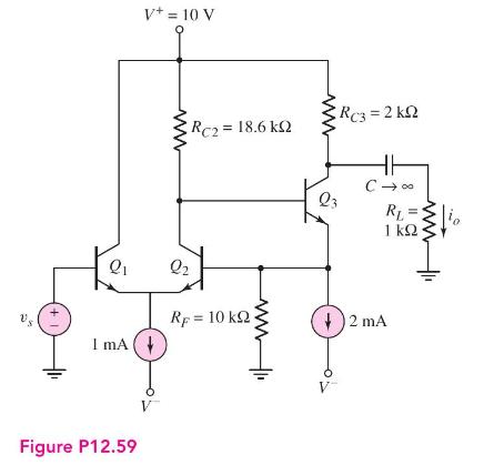
In the circuit in Figure P12.59, the transistor parameters are: \(h_{F E}=100\), \(V_{B E}(\mathrm{on})=0.7 \mathrm{~V}\), and \(V_{A}=\infty\). Determine the transconductance transfer function \(A_{g f}=i_{o} / v_{s}\). + V+= 10 V Rc3 = 2 k Rc2 = 18.6 k 1 mA + Q2 Rp 10 k Figure P12.59 23 R = 1 +
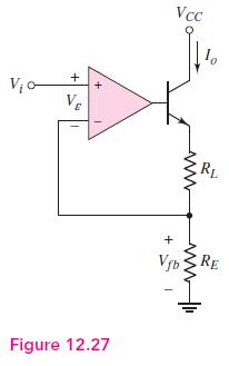
Design a feedback amplifier to supply a current to an LED. Use the configuration shown in Figure 12.27 where \(R_{L}\) is replaced by the LED. (a) Assuming an ideal op-amp is available, design the circuit such that the diode current is \(I_{O}=3 \times 10^{-3} V_{i}\) where \(V_{i}\) is in the
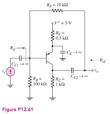
Consider the common-emitter circuit in Figure P12.61 driven by an ideal signal current source. The transistor parameters are \(h_{F E}=80, V_{E B}(\) on \()=0.7 \mathrm{~V}\), and \(V_{A}=100 \mathrm{~V}\). (a) Determine the quiescent values \(I_{C Q}\) and \(V_{E C Q}\). (b) Find the
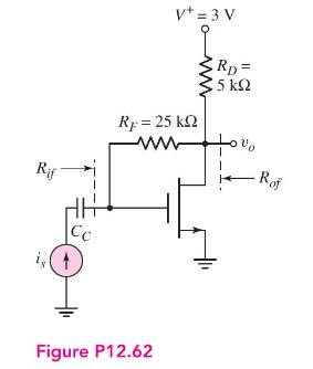
The transistor parameters for the circuit shown in Figure P12.62 are \(V_{T N}=\) \(0.4 \mathrm{~V}, K_{n}=0.5 \mathrm{~mA} / \mathrm{V}^{2}\), and \(\lambda=0\). (a) Find (i) the quiescent drain current \(I_{D Q}\) and (ii) the small-signal transistor parameters. (b) Determine the transresistance
Consider Problem 12.62. (a) What is the magnitude of the ideal transresistance transfer function \(\left|A_{z f}\right|\) as the transistor transconductance parameter \(g_{m} \rightarrow \infty\). (b) Determine the value of \(g_{m}\) so that \(\left|A_{z f}\right|\) is within 95 percent of the
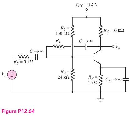
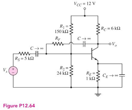
For the circuit in Figure P12.64, the transistor parameters are: \(h_{F E}=150\), \(V_{B E}(\) on \()=0.7 \mathrm{~V}\), and \(V_{A}=\infty\). Determine the value of \(R_{F}\) that will result in a closed-loop voltage gain of \(A_{v}=V_{o} / V_{s}=-5.0\). ww Rs = 5kQ Figure P12.64 R =2 150 Vcc =
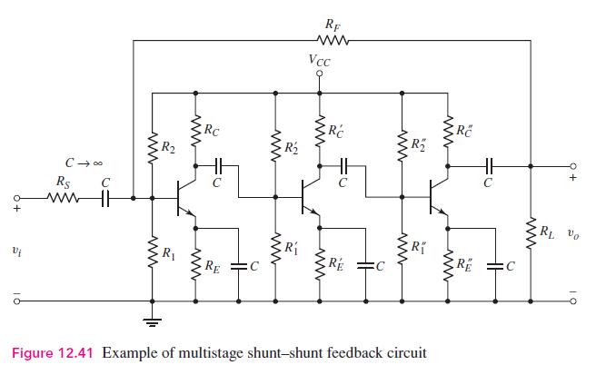
Consider the three-stage cascade feedback circuit in Figure 12.41. Each stage corresponds to the circuit in Figure P12.65, with transistor parameters: \(h_{F E}=180, V_{B E}\) (on) \(=0.7 \mathrm{~V}\), and \(V_{A}=\infty\). The source resistor is \(R_{S}=10 \mathrm{k} \Omega\), and the load
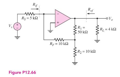
The op-amp in the circuit in Figure P12.66 has an open-loop differential voltage gain of \(A_{d}=10^{4}\). Neglect the current into the op-amp, and assume the output resistance looking back into the op-amp is zero. Determine: (a) the closed-loop voltage gain \(A_{v}=V_{o} / V_{s}\), (b) the input
Design a feedback transresistance amplifier using an op-amp with parameters \(R_{i}=10 \mathrm{k} \Omega, R_{o}=100 \Omega\), and a low-frequency open-loop gain of \(A_{v}=10^{4}\) to produce a gain of \(5 \mathrm{k} \Omega\). The source resistance is \(R_{S}=500 \Omega\) and the load resistance is
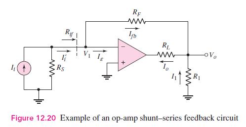
The op-amp in Figure 12.20 has an open-loop differential input resistance \(R_{i}\), an open-loop current gain \(A_{i}\), and a zero output resistance. Break the feedback loop at an appropriate point, and derive the expression for the loop gain. Rs RF ww Rif Ifb R ww R Figure 12.20 Example of an
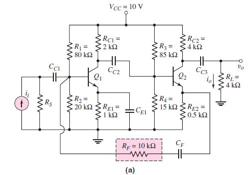
The small-signal parameters of the transistors in the circuit in Figure P12.37 are \(h_{F E}\) and \(V_{A}=\infty\). Derive the expression for the loop gain. Cc Rif Vi ww ww R = 400 R = 75 www ww Vcc = 10 V RC1= 8.8 Rc2= 13 Q3 Q2 REI= 0.5 CE RE2= 13.6 RE3 = 1.4 k Figure P12.37 ww RF = 10 HH
Determine the loop gain \(T\) for the circuit in Figure P12.49. The transistor parameters are: \(h_{F E}=100, V_{B E}(\mathrm{on})=0.7 \mathrm{~V}\), and \(V_{A}=\infty\). is Rif V+=+10 V ww RCI = 40 k Rs = 10 EI= 0.2 mA ww ww Q2 Rc2 = 2 k HH C Figure P12.49 V-=-10 V ww RF = 10 k RE= 1 ww www HH
The transistor parameters for the circuit shown in Figure P12.64 are: \(h_{F E}=50, V_{B E}\) (on) \(=0.7 \mathrm{~V}\), and \(V_{A}=100 \mathrm{~V}\). Find the loop gain \(T\). Vcc=12 V ww-h Rs = 5kQ R = 150 RF ww +- Figure P12.64 ww R = 24 Rc=6kQ -OV www RE= 1 CE
A three-pole feedback amplifier has a loop gain given by\[T(f)=\frac{\beta\left(5 \times 10^{4}\right)}{\left(1+j \frac{f}{10^{3}}\right)\left(1+j \frac{f}{5 \times 10^{4}}\right)^{2}}\](a) Determine the frequency \(f_{180}\) at which the phase is -180 degrees. (b) At the frequency \(f_{180}\),
The open-loop voltage gain of an amplifier is given by\[A_{v}=\frac{10^{4}}{\left(1+j \frac{f}{5 \times 10^{3}}\right)^{2}\left(1+j \frac{f}{5 \times 10^{5}}\right)}\](a) Assuming the feedback transfer function is not a function of frequency, determine the frequency at which the phase of the loop
A loop gain function is given by\[T(f)=\frac{\beta\left(10^{3}\right)}{\left(1+j \frac{f}{10^{4}}\right)\left(1+j \frac{f}{5 \times 10^{4}}\right)\left(1+j \frac{f}{10^{5}}\right)}\]Sketch the Nyquist plot for: (a) \(\beta=0.005\), and (b) \(\beta=0.05\). (c) Is the system stable or unstable in
A three-pole feedback amplifier has a loop gain function given by\[T(f)=\frac{\beta\left(5 \times 10^{3}\right)}{\left(1+j \frac{f}{10^{3}}\right)^{2}\left(1+j \frac{f}{5 \times 10^{4}}\right)}\](a) Sketch the Nyquist diagram for \(\beta=0.20\). (b) Determine the value of \(\beta\) that produces a
A three-pole feedback amplifier has a loop gain given by\[T(f)=\frac{\beta\left(10^{4}\right)}{\left(1+j \frac{f}{10^{3}}\right)\left(1+j \frac{f}{10^{4}}\right)\left(1+j \frac{f}{10^{5}}\right)}\]Sketch Bode plots of the loop gain magnitude and phase for: (a) \(\beta=0.005\), and (b)
A feedback system has an amplifier with a low-frequency open-loop gain of \(5 \times 10^{4}\) and has poles at \(10^{3} \mathrm{~Hz}, 10^{5} \mathrm{~Hz}\), and \(10^{7} \mathrm{~Hz}\). (a) Determine the frequency \(f_{180}\) at which the phase of the loop gain is 180 degrees. (b) Determine the
The open-loop voltage gain of an amplifier is given by\[A_{v}=\frac{10^{5}}{\left(1+j \frac{f}{10^{3}}\right)\left(1+j \frac{f}{10^{5}}\right)}\](a) If the low-frequency, closed-loop gain is 100 , is this amplifier stable?(b) If so, determine the phase margin.
The loop gain function of a feedback system is described by\[T(f)=\frac{\beta\left(10^{3}\right)}{\left(1+j \frac{f}{10^{4}}\right)\left(1+j \frac{f}{10^{5}}\right)\left(1+j \frac{f}{10^{6}}\right)}\](a) Determine the frequency \(f_{180}\) at which the phase of \(T(f)\) is -180 degrees. (b) For
Consider a feedback amplifier for which the open-loop gain is given by\[A(f)=\frac{2 \times 10^{3}}{\left(1+j \frac{f}{5 \times 10^{3}}\right)\left(1+j \frac{f}{10^{5}}\right)^{2}}\](a) Determine the frequency \(f_{180}\) at which the phase of \(A(f)\) is -180 degrees.(b) For \(\beta=0.0045\),
Consider a four-pole feedback system with a loop gain given by\[T(f)=\frac{\beta\left(10^{3}\right)}{\left(1+j \frac{f}{10^{3}}\right)\left(1+j \frac{f}{10^{4}}\right)\left(1+j \frac{f}{10^{5}}\right)\left(1+j \frac{f}{10^{6}}\right)}\]Determine the value of \(\beta\) that produces a phase margin
A feedback amplifier has a low-frequency open-loop gain of 4000 and three poles at \(f_{P 1}=400 \mathrm{kHz}, f_{P 2}=4 \mathrm{MHz}\), and \(f_{P 3}=40 \mathrm{MHz}\). A dominant pole is to be inserted such that the phase margin is 60 degrees. Assuming the original poles remain fixed, determine
The loop gain of a three-pole amplifier is given by\[T(f)=\frac{10^{3}}{\left(1+j \frac{f}{10^{4}}\right)^{2}\left(1+j \frac{f}{10^{6}}\right)}\](a) Show that this function will lead to an unstable feedback system. (b) Insert a dominant pole such that the phase margin is 45 degrees. Assume the
A loop gain function is given by\[T(f)=\frac{500}{\left(1+j \frac{f}{10^{4}}\right)\left(1+j \frac{f}{5 \times 10^{4}}\right)\left(1+j \frac{f}{10^{5}}\right)}\](a) Determine the frequency \(f_{180}\) (to a good approximation) at which the phase of \(T(f)\) is -180 degrees. (b) What is the
An open-loop amplifier can be described by\[A_{v}=\frac{10^{4}}{\left(1+j \frac{f}{10^{5}}\right)}\]A dominant pole is to be inserted such that a closed-loop amplifier with a low-frequency gain of 50 has a phase margin of 45 degrees.(a) Determine \(\beta\) and the required dominant pole
The open-loop amplifier of a feedback system has its first two poles at \(f_{P 1}=1\) \(\mathrm{MHz}\) and \(f_{P 2}=10 \mathrm{MHz}\), and has a low-frequency open-loop gain of \(\left|A_{o}\right|=100 \mathrm{~dB}\).(a) A dominant pole is to be added such that the closed-loop amplifier with a
A feedback amplifier with a compensation capacitor has a low-frequency loop gain of \(T(0)=100 \mathrm{~dB}\) and poles at \(f_{P 1}^{\prime}=10 \mathrm{~Hz}, f_{P 2}=5 \mathrm{MHz}\), and \(f_{P 3}=10 \mathrm{MHz}\). (a) Find the frequency at which \(|T(f)|=1\), and determine the phase margin. (b)
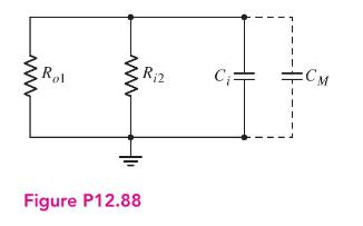
The equivalent circuit at the interface between the first and second stages of an op-amp is shown in Figure P12.88. The parameters are \(R_{o 1}=2 \mathrm{M} \Omega\), \(R_{i 2}=750 \mathrm{k} \Omega\), and \(C_{i}=1.2 \mathrm{pF}\). (a) Determine the pole frequency for this part of the circuit.
The amplifier described in Problem 12.82 is to be stabilized by moving the first pole by using Miller compensation. Assuming that \(f_{P 2}\) and \(f_{P 3}\) remain fixed, determine the frequency to which \(f_{P 1}\) must be moved such that the phase margin is 60 degrees.Data From Problem 12.82:-A
The loop gain of an amplifier is given by\[T(f)=\frac{\beta\left(5 \times 10^{5}\right)}{\left(1+j \frac{f}{10^{4}}\right)\left(1+j \frac{f}{5 \times 10^{5}}\right)\left(1+j \frac{f}{10^{7}}\right)}\]The pole at \(f_{P 1}=10^{4}\) is to be moved such that the feedback amplifier with a closed-loop
Consider the circuit shown in Figure 12.24(a). Replace the input signal source with an ideal signal voltage source. Using a computer simulation, investigate the small-signal voltage gain, input resistance \(R_{i f}\), and output resistance \(R_{o f}\) as a function of the feedback resistance
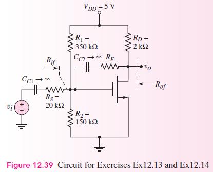
For the circuit shown in Figure 12.39, investigate the small-signal voltage gain, input resistance, and output resistance as a function of the transistor width-to-length ratio, using a computer simulation.Figure 12.39:- vi VDD = 5 V Rif HH ww Rs = 20 R = 350 Cc2RF ww RD= 2 +1 R = 150 - Rof
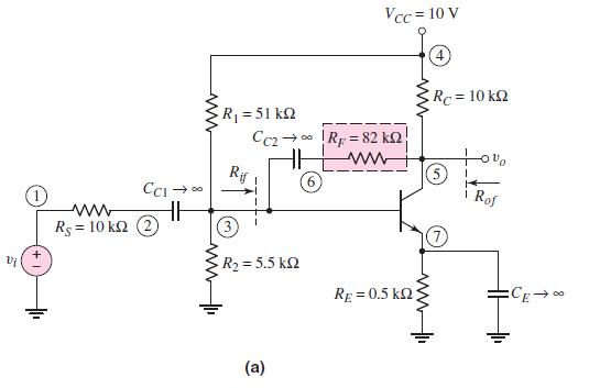
Consider the circuit shown in Figure 12.37(a). Using a computer simulation, plot the loop gain as a function of frequency.Figure 12.37(a):- Vj ww Rs = 10 k CC1 2 Vcc = 10 V Rc = 10 R = = 51 Rif (3) CC2 R = 5.5 k ww 00 = Rp 82 k (5) Rof RE=0.5 k www (a)
In the circuit shown in Figure P12.42, use a computer simulation to plot the small-signal voltage gain versus frequency. Determine the low-frequency and high-frequency cutoff values. Vs C = 5 F HH 47 ww ww +25 V 150 V ww 10 HH C2= 21 5 F 4.7 Figure P12.42 www C3= 50 F R = 100 ww ww 47 33
The circuit shown in Figure P12.46 is to have a minimum loop gain of \(T=200\). Design the width-to-length ratios of the transistors to meet this requirement. Use appropriate transistor parameters. V+= 10 V M VG = 7.6 V RDI = 525 2 ww M2 Figure P12.46 ww Rp = 500 2 LED Rp2= 250
Op-amps with low-frequency open-loop gains of \(5 \times 10^{4}\) and dominantpole frequencies of \(8 \mathrm{~Hz}\) are available. Design a cascade of noninverting amplifiers such that the overall voltage gain is 500 and the bandwidth is \(15 \mathrm{kHz}\)
An op-amp has a low-frequency open-loop gain of \(5 \times 10^{4}\) and a dominantpole frequency of \(10 \mathrm{~Hz}\). Using this op-amp, design a preamplifier system that can amplify the output of a microphone and produce a \(1 \mathrm{~V}\) peak signal over a frequency range from \(10
The equivalent circuit of a transducer that measures the speed of a motor is a current source in parallel with an output resistance. The current source produces an output of \(1 \mu \mathrm{A}\) per revolution per second of the motor and the output resistance is \(50 \mathrm{k} \Omega\). Design a
Describe the principal stages of a general-purpose operational amplifier.
What is meant by the term matched transistors? What parameters in BJTs and MOSFETs are identical in matched devices?
Describe the operation and characteristics of a BJT complementary push-pull output stage. What are the advantages of this circuit?
Describe the operation and characteristics of a MOSFET complementary push-pull output stage. What are the advantages of this circuit?
Describe the configuration and operation of the input diff-amp stage of the 741 op-amp.
What is the purpose of the resistor \(R_{3}\) in the active load of the 741 op-amp?
Describe the configuration of the output stage of the 741 op-amp.
Describe the operation of the short-circuit protection circuitry in the 741 op-amp.
Describe the frequency compensation technique in the \(741 \mathrm{op}-\mathrm{amp}\) circuit.
Sketch and describe the general characteristics of a folded cascode circuit.
Sketch and describe the general characteristics of a current-mirror op-amp circuit. Why is the gain not increased? What is the principal advantage of this circuit?
Sketch and describe the principal advantage of a BiCMOS folded cascode opamp circuit.
Explain why an output resistance on the order of five hundred megohms may not be achieved in practice.
What are the principal factors limiting the unity-gain bandwidth of an op-amp circuit?
Showing 500 - 600
of 4723
1
2
3
4
5
6
7
8
9
10
11
12
13
14
15
Last
Step by Step Answers