New Semester
Started
Get
50% OFF
Study Help!
--h --m --s
Claim Now
Question Answers
Textbooks
Find textbooks, questions and answers
Oops, something went wrong!
Change your search query and then try again
S
Books
FREE
Study Help
Expert Questions
Accounting
General Management
Mathematics
Finance
Organizational Behaviour
Law
Physics
Operating System
Management Leadership
Sociology
Programming
Marketing
Database
Computer Network
Economics
Textbooks Solutions
Accounting
Managerial Accounting
Management Leadership
Cost Accounting
Statistics
Business Law
Corporate Finance
Finance
Economics
Auditing
Tutors
Online Tutors
Find a Tutor
Hire a Tutor
Become a Tutor
AI Tutor
AI Study Planner
NEW
Sell Books
Search
Search
Sign In
Register
study help
computer science
systems analysis and design 12th
Microelectronics Circuit Analysis And Design 4th Edition Donald A. Neamen - Solutions
(a) A differential-amplifier has a differential-mode gain of \(A_{d}=250\) and a common-mode rejection ratio of \(\mathrm{CMRR}_{\mathrm{dB}}=\infty\). A differential-mode input signal of \(v_{d}=1.5 \sin \omega t \mathrm{mV}\) is applied along with a common-mode input signal of \(v_{c m}=3 \sin
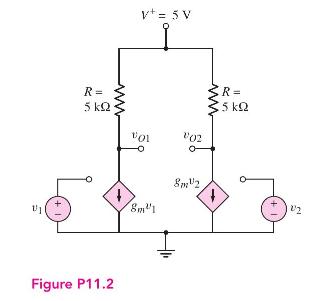
Consider the circuit shown in Figure P11.2. Assume \(g_{m}=1.0 \mathrm{~mA} / \mathrm{V}\). Assume the input signal voltages are \(v_{1}=0.7+0.1 \sin \omega t \mathrm{~V}\) and \(v_{2}=\) \(0.7-0.1 \sin \omega t \mathrm{~V}\). (a) Determine the signal voltages (i) \(v_{o 1}\), (ii) \(v_{o 2}\), and
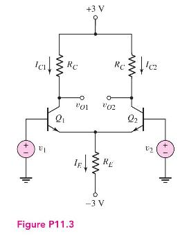
Consider the differential amplifier shown in Figure P11.3 with transistor parameters \(\beta=150, V_{B E}(\) on \()=0.7 \mathrm{~V}\), and \(V_{A}=\infty\). (a) Design the circuit such that the \(Q\)-point values are \(I_{C 1}=I_{C 2}=100 \mu \mathrm{A}\) and \(v_{O 1}=\) \(v_{O 2}=1.2
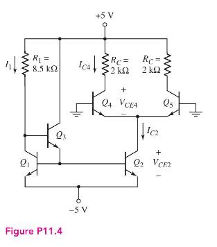
The differential amplifier in Figure P11.4 is biased with a three-transistor current source. The transistor parameters are: \(\beta=100, V_{B E}(\) on \()=0.7 \mathrm{~V}\), and \(V_{A}=\infty\). (a) Determine \(I_{1}, I_{C 2}, I_{C 4}, V_{C E 2}\), and \(V_{C E 4}\). (b) Determine a new value of
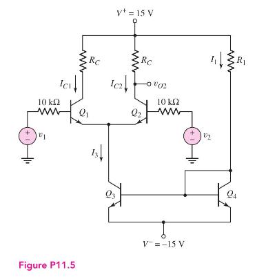
For the transistors in the circuit in Figure P11.5, the parameters are \(\beta=100\) and \(V_{B E}(\mathrm{on})=0.7 \mathrm{~V}\). The Early voltage is \(V_{A}=\infty\) for \(Q_{1}\) and \(Q_{2}\), and is \(V_{A}=50 \mathrm{~V}\) for \(Q_{3}\) and \(Q_{4}\). (a) Design resistor values such that
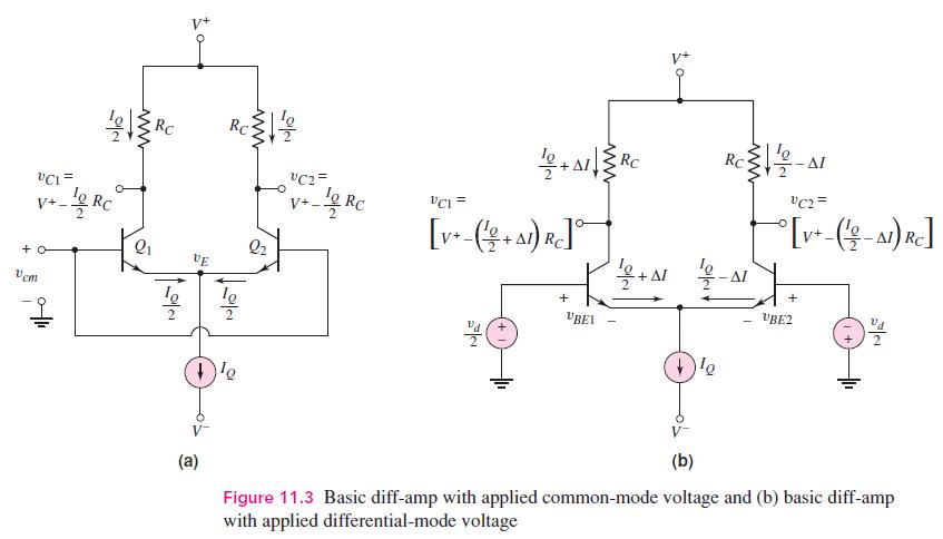
The diff-amp in Figure 11.3 of the text has parameters \(V^{+}=+5 \mathrm{~V}\), \(V^{-}=-5 \mathrm{~V}, R_{C}=8 \mathrm{k} \Omega\), and \(I_{Q}=0.5 \mathrm{~mA}\). The transistor parameters are \(\beta=120, V_{B E}\) (on) \(=0.7 \mathrm{~V}\), and \(V_{A}=\infty\).(a) Using Figure 11.3(a),
The diff-amp configuration shown in Figure P11.7 is biased at \(\pm 3 \mathrm{~V}\). The maximum power dissipation in the entire circuit is to be no more than \(1.2 \mathrm{~mW}\) when \(v_{1}=v_{2}=0\). The available transistors have parameters: \(\beta=120, V_{B E}\) (on) \(=0.7 \mathrm{~V}\),
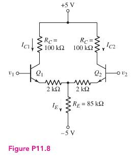
Consider the circuit in Figure P11.8, with transistor parameters: \(\beta=100\), \(V_{B E}\) (on) \(=0.7 \mathrm{~V}\), and \(V_{A}=\infty\). (a) For \(v_{1}=v_{2}=0\), find \(I_{C 1}, I_{C 2}, I_{E}, V_{C E 1}\), and \(V_{C E 2}\). (b) Determine the maximum and minimum values of the common-mode
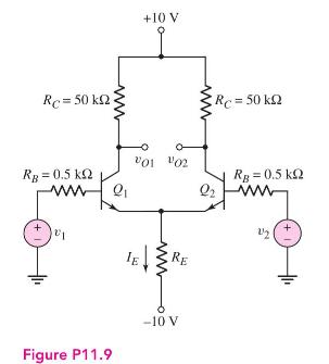
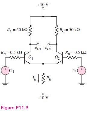
The transistor parameters for the circuit in Figure P11.9 are: \(\beta=100\), \(V_{B E}(\mathrm{on})=0.7 \mathrm{~V}\), and \(V_{A}=\infty\). (a) Determine \(R_{E}\) such that \(I_{E}=150 \mu \mathrm{A}\). (b) Find \(A_{d}, A_{c m}\), and \(\mathrm{CMRR}_{\mathrm{dB}}\) for a one-sided output at
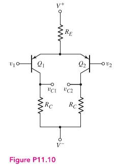
The bias voltages for the diff-amp shown in Figure P11.10 are \(V^{+}=3 \mathrm{~V}\) and \(V^{-}=-3 \mathrm{~V}\). The transistor current gains are \(\beta=80\), the nominal value of \(V_{B E}\left(\right.\) on) is \(0.6 \mathrm{~V}\), and \(V_{A}=\infty\). (a) Design the circuit such that the
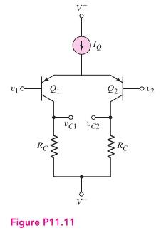
Consider the circuit shown in Figure P11.11. The circuit and transistor parameters are \(V^{+}=+3 \mathrm{~V}, V^{-}=-3 \mathrm{~V}, R_{C}=360 \mathrm{k} \Omega, I_{Q}=12 \mu \mathrm{A}\), \(\beta=60, V_{E B}\) (on) \(=0.6 \mathrm{~V}\), and \(V_{A}=\infty\). The output resistance of the current
The circuit and transistor parameters for the circuit shown in Figure P11.11 are \(V^{+}=5 \mathrm{~V}, V^{-}=-5 \mathrm{~V}, I_{Q}=0.2 \mathrm{~mA}, \beta=80, V_{E B}(\) on \()=0.6 \mathrm{~V}\), and \(V_{A}=\infty\). (a) Design the circuit such that the minimum common-mode voltage is \(v_{c
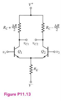
Consider the differential amplifier shown in Figure P11.13 with mismatched collector resistors. The circuit and transistor parameters are \(V^{+}=5 \mathrm{~V}\), \(V^{-}=-5 \mathrm{~V}, \beta=120, V_{B E}(\) on \()=0.7 \mathrm{~V}\), and \(V_{A}=\infty\). (a) For \(\Delta R=0\), design the circuit
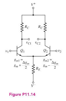
Consider the differential amplifier shown in Figure P11.14 with mismatched transistors. The mismatched transistors result in mismatched transconductances as shown. The circuit and transistor parameters are \(V^{+}=+10 \quad \mathrm{~V}, V^{-}=-10 \quad \mathrm{~V}, R_{C}=50 \mathrm{k} \Omega,
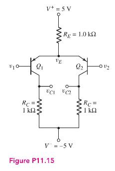
Consider the circuit in Figure P11.15. The transistor parameters are \(\beta=120, V_{E B}\) (on) \(=0.7 \mathrm{~V}\), and \(V_{A}=\infty\). Determine \(v_{E}, v_{C 1}\), and \(v_{C 2}\) for (a) \(v_{1}=v_{2}=0\); (b) \(v_{1}=0.5 \mathrm{~V}, v_{2}=0\); and (c) \(v_{1}=0, v_{2}=0.015 \mathrm{~V}\).
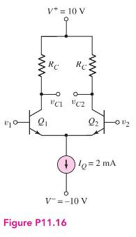
(a) Design the circuit shown in Figure P11.16 such that \(v_{O}=\) \(v_{C 1}-v_{C 2}=1 \mathrm{~V}\) when \(v_{1}=-5 \mathrm{mV}\) and \(v_{2}=+5 \mathrm{mV}\). The transistor parameters are \(\beta=180, V_{B E}(\) on \()=0.7 \mathrm{~V}\), and \(V_{A}=\infty\). (b) Using the results of part (a),
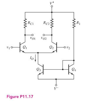
Consider the differential amplifier in Figure P11.17 with parameters \(V^{+}=5 \mathrm{~V}, V^{-}=-5 \mathrm{~V}\), and \(I_{O}=0.8 \mathrm{~mA}\). Neglect base currents and assume \(V_{A}=\infty\) for all transistors. The emitter currents can be written as \(I_{E 1}=I_{S 1} e^{V_{B E 1} / V_{T}}\)
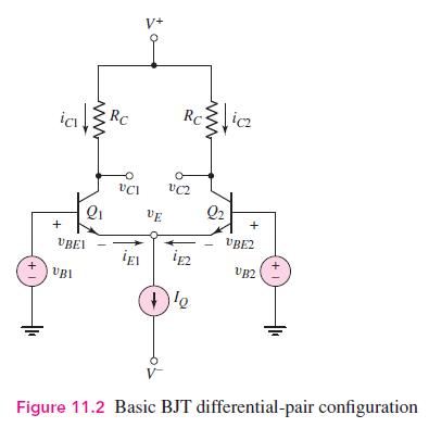
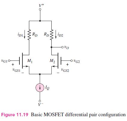
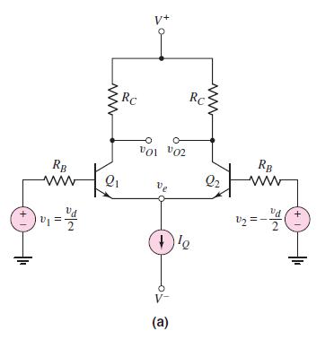
For the diff-amp in Figure 11.2, determine the value of \(v_{d}=v_{1}-v_{2}\) that produces (a) \(i_{C 1}=0.20 I_{Q}\) and (b) \(i_{C 2}=0.90 I_{Q}\).Figure 11.2:- V+ ww ic RC Rc icz UCI UC2 Q1 VE 22 + + UBE2 UBEI EI iF2 UB2 UBI +- +1 Figure 11.2 Basic BJT differential-pair configuration
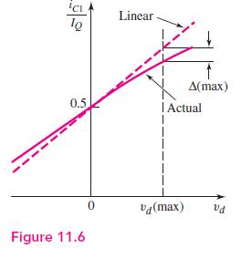
Consider the expanded dc transfer curves shown in Figure 11.6. Determine the maximum differential input voltage such that the actual curve is within (a) 0.5 percent of the ideal linear extrapolation and (b) 1.5 percent of the ideal extrapolation.Figure 11.6:- iCI Linear IQ 0.5 Figure 11.6 A(max) |
The diff-amp for the experimental system described in Example 11.4 needs to be redesigned. The range of the output voltage has increased to \(-2 \leq V_{O} \leq 2 \mathrm{~V}\) while the differential-mode voltage gain is still \(A_{d}=100\). The common-mode input voltage has increased to \(v_{C
The transistor parameters for the circuit in Figure P11.9 are: \(\beta=120\), \(V_{B E}\) (on) \(=0.7 \mathrm{~V}\), and \(V_{A}=\infty\). (a) Determine \(R_{E}\) such that \(I_{E}=0.25 \mathrm{~mA}\). (b) Assume the \(R_{B}\) resistance connected to the base of \(Q_{2}\) is zero while the
The circuit parameters of the diff-amp shown in Figure 11.2 are \(V^{+}=3 \mathrm{~V}, V^{-}=-3 \mathrm{~V}\), and \(I_{Q}=0.25 \mathrm{~mA}\). Base currents are negligible and \(V_{A}=\infty\) for each transistor. (a) Design the circuit such that a differential-mode output voltage of \(v_{o}=v_{C
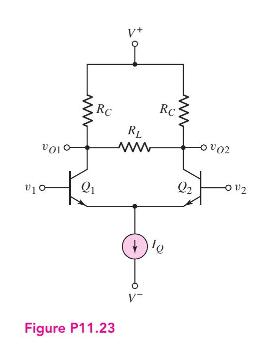
Consider the circuit in Figure P11.23. Assume the Early voltage of \(Q_{1}\) and \(Q_{2}\) is \(V_{A}=\infty\), and assume the current source \(I_{Q}\) is ideal. Derive the expressions for the one-sided differential-mode gain \(A_{v 1}=v_{o 1} / v_{d}\) and \(A_{v 2}=v_{o 2} / v_{d}\), and for the
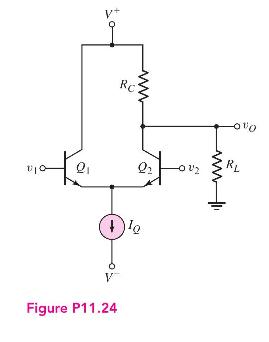
The Early voltage of transistors \(Q_{1}\) and \(Q_{2}\) in the circuit in Figure P11.24 is \(V_{A}=\infty\). Assuming an ideal current source \(I_{Q}\), derive the expression for the differential-mode gain \(A_{d}=v_{o} / v_{d}\). RC -01/0 K RL Figure P11.24
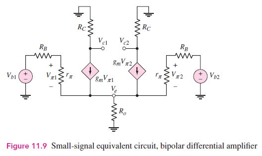
Consider the small-signal equivalent circuit of the differential-pair configuration shown in Figure 11.9. Derive the expressions for the differential and common-mode voltage gains if the output is a two-sided output defined as \(V_{o}=V_{c 2}-V_{c 1}\). Rc Vc2 Rc RB RB 8mVx2 + + V x2 Vb2 8mVx1 Vbl
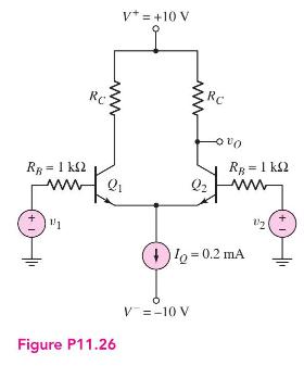
Consider a BJT diff-amp with the configuration in Figure P11.26. The signal sources have nonzero source resistances as shown. The transistor parameters are: \(\beta=150, V_{B E}\) (on) \(=0.7 \mathrm{~V}\), and \(V_{A}=\infty\). The range of the common-mode input voltage is to be \(-3 \leq v_{C M}
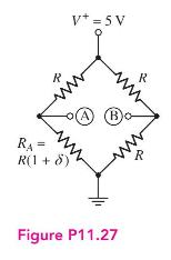
The bridge circuit in Figure P11.27 is a temperature transducer in which the resistor \(R_{A}\) is a thermistor (a resistor whose resistance varies with temperature). The value of \(\delta\) varies over the range of \(-0.01 \leq \delta \leq 0.01\) as temperature varies over a particular range.
A diff-amp is biased with a constant-current source \(I_{Q}=0.25 \mathrm{~mA}\) that has an output resistance of \(R_{o}=8 \mathrm{M} \Omega\). The bipolar transistor parameters are \(\beta=120\) and \(V_{A}=\infty\). Determine (a) the differential-mode input resistance and (b) the common-mode
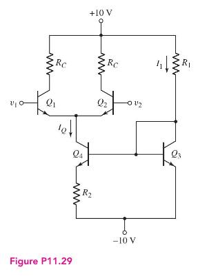
The transistor parameters for the circuit shown in Figure P11.29 are \(\beta=180, V_{B E}\) (on) \(=0.7 \mathrm{~V}\) (except for \(\left.Q_{4}\right), V_{A}=\infty\) for \(Q_{1}\) and \(Q_{2}\), and \(V_{A}=100 \mathrm{~V}\) for \(Q_{3}\) and \(Q_{4}\). (a) Determine \(R_{1}\) and \(R_{2}\) such
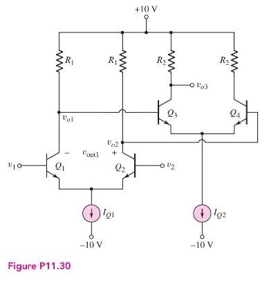
Figure P11.30 shows a two-stage cascade diff-amp with resistive loads. Power supply voltages of \(\pm 10 \mathrm{~V}\) are available. Assume transistor parameters of: \(\beta=100, V_{B E}\) (on) \(=0.7 \mathrm{~V}\), and \(V_{A}=\infty\). Design the circuit such that the two-sided differential-mode
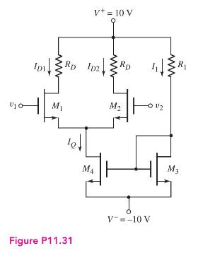
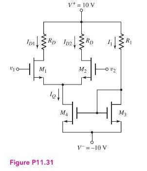
For the differential amplifier in Figure P11.31 the parameters are \(R_{1}=50 \mathrm{k} \Omega\) and \(R_{D}=24 \mathrm{k} \Omega\). The transistor parameters are: \(K_{n}=0.25 \mathrm{~mA} / \mathrm{V}^{2}, \lambda=0\), and \(V_{T N}=2 \mathrm{~V}\). (a) Determine \(I_{1}, I_{Q}, I_{D 1}, V_{D S
The bias voltages in the diff-amp shown in Figure P11.31 are changed to \(V^{+}=3 \mathrm{~V}\) and \(V^{-}=-3 \mathrm{~V}\). The transistor parameters are \(K_{n 1}=K_{n 2}=\) \(100 \mu \mathrm{A} / \mathrm{V}^{2}, K_{n 3}=K_{n 4}=200 \mu \mathrm{A} / \mathrm{V}^{2}, \lambda_{1}=\lambda_{2}=0,
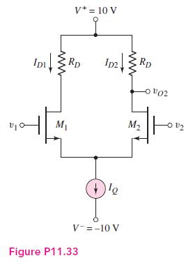
The transistor parameters for the differential amplifier shown in Figure \(\mathrm{P} 11.33\) are \(V_{T N}=0.5 \mathrm{~V}, k_{n}^{\prime}=80 \mu \mathrm{A} / \mathrm{V}^{2}, W / L=4\), and \(\lambda=0\). (a) Find \(R_{D}\) and \(I_{Q}\) such that \(I_{D 1}=I_{D 2}=80 \mu \mathrm{A}\) and \(v_{O
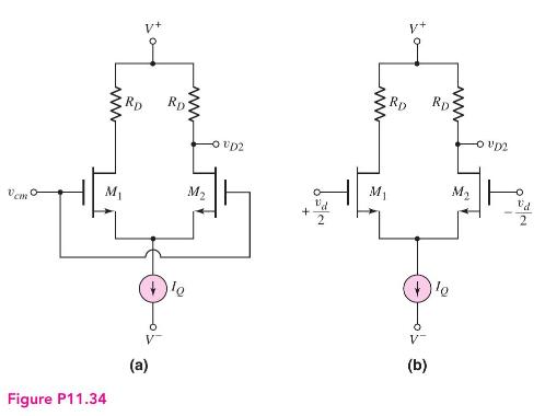
The diff-amp in Figure P11.34 has parameters \(V^{+}=3 \mathrm{~V}, V^{-}=-3 \mathrm{~V}\), and \(I_{Q}=0.18 \mathrm{~mA}\). The transistor parameters are \(V_{T N}=0.35 \mathrm{~V}, k_{n}^{\prime}=\) \(100 \mu \mathrm{A} / \mathrm{V}^{2}, W / L=4\), and \(\lambda=0\). (a) Using Figure P11.34(a),
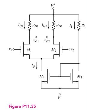
The bias voltages of the diff-amp shown in Figure \(\mathrm{P} 11.35\) are \(V^{+}=5 \mathrm{~V}\) and \(V^{-}=-5 \mathrm{~V}\). The threshold voltage of each transistor is \(V_{T N}=0.4 \mathrm{~V}\) and assume \(\lambda=0\). Let \(K_{n 3}=K_{n 4}=0.20 \mathrm{~mA} / \mathrm{V}^{2}\). The drain
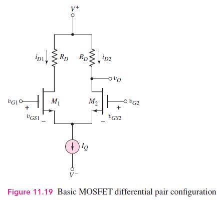
The circuit parameters of the diff-amp shown in Figure 11.19 are \(V^{+}=3 \mathrm{~V}, V^{-}=-3 \mathrm{~V}\), and \(I_{Q}=0.15 \mathrm{~mA}\). The transistor parameters are \(K_{n}=0.2 \mathrm{~mA} / \mathrm{V}^{2}, V_{T N}=0.4 \mathrm{~V}\), and \(\lambda=0\). Determine the value of \(v_{d}=\)
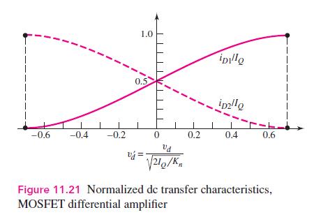
Consider the normalized dc transfer characteristics of a MOSFET diff-amp shown in Figure 11.21. Assume that \(K_{n}=0.20 \mathrm{~mA} / \mathrm{V}^{2}\) and \(I_{Q}=0.10 \mathrm{~mA}\). Determine the maximum differential input voltage such that the actual curve of \(i_{D 1} / I_{Q}\) is within (a)
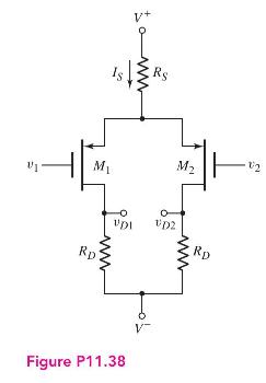
The parameters of the diff-amp circuit shown in Figure P11.38 are \(V^{+}=9 \mathrm{~V}\), \(V^{-}=-9 \mathrm{~V}, R_{D}=510 \mathrm{k} \Omega\), and \(R_{S}=390 \mathrm{k} \Omega\). The transistor parameters are \(V_{T P}=-0.8 \mathrm{~V}, K_{p}=50 \mu \mathrm{A} / \mathrm{V}^{2}\), and
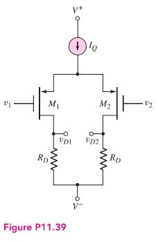
Consider the circuit shown in Figure P11.39. The circuit and transistor parameters are \(V^{+}=+3 \mathrm{~V}, V^{-}=-3 \mathrm{~V}, R_{D}=360 \mathrm{k} \Omega, I_{Q}=12 \mu \mathrm{A}\), \(V_{T P}=-0.4 \mathrm{~V}, K_{p}=30 \mu \mathrm{A} / \mathrm{V}^{2}\), and \(\lambda=0\). The output
The circuit and transistor parameters for the circuit shown in Figure P11.39 are \(V^{+}=5 \mathrm{~V}, V^{-}=-5 \mathrm{~V}, I_{Q}=0.15 \mathrm{~mA}, R_{D}=30 \mathrm{k} \Omega, V_{T P}=-0.5 \mathrm{~V}\), \(K_{p}=0.12 \mathrm{~mA} / \mathrm{V}^{2}\), and \(\lambda=0\). The output resistance of
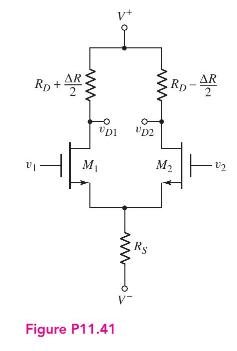
Consider the differential amplifier shown in Figure P11.41 with mismatched drain resistors. The circuit and transistor parameters are \(V^{+}=\) \(+10 \mathrm{~V}, V^{-}=-10 \mathrm{~V}, R_{D}=50 \mathrm{k} \Omega, R_{S}=75 \mathrm{k} \Omega, V_{T N}=1 \mathrm{~V}, K_{n}=\) \(0.15 \mathrm{~mA} /
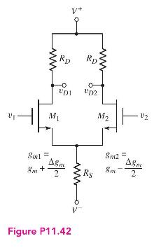
Consider the differential amplifier shown in Figure P11.42 with mismatched transistors. The mismatched transistors result in mismatched transconductances as shown. The circuit and transistor parameters are \(V^{+}=+10 \mathrm{~V}, V^{-}=-10 \mathrm{~V}, R_{D}=50 \mathrm{k} \Omega, R_{S}=75
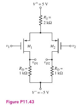
Consider the circuit in Figure P11.43. The transistor parameters are \(K_{p}=1.2 \mathrm{~mA} / \mathrm{V}^{2}, V_{T P}=-0.6 \mathrm{~V}\), and \(\lambda=0\). Determine \(v_{S}, v_{D 1}\), and \(v_{D 2}\) for (a) \(v_{1}=v_{2}=0\); (b) \(v_{1}=v_{2}=1 \mathrm{~V}\); (c) \(v_{1}=-0.1 \mathrm{~V},
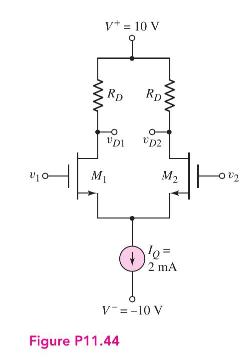
(a) Design the circuit shown in Figure P11.44 such that \(v_{O}=v_{D 1}-v_{D 2}=\) \(1 \mathrm{~V}\) when \(v_{1}=-50 \mathrm{mV}\) and \(v_{2}=+50 \mathrm{mV}\). The transistor parameters are \(V_{T N}=0.8 \mathrm{~V}, K_{n}=0.4 \mathrm{~mA} / \mathrm{V}^{2}\), and \(\lambda=0\). (b) Using the
The Hall effect experimental arrangement was described in Example 11.4. The required diff-amp is to be designed in the circuit configuration in Figure P11.35. The transistor parameters are \(V_{T N}=0.8 \mathrm{~V}, k_{n}^{\prime}=80 \mu \mathrm{A} / \mathrm{V}^{2}\), \(\lambda_{1}=\lambda_{2}=0\),
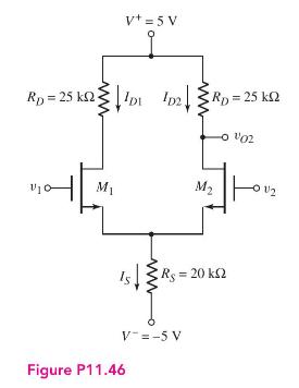
Consider the diff-amp in Figure P11.46. The transistor parameters are: \(K_{n 1}=K_{n 2}=50 \mu \mathrm{A} / \mathrm{V}^{2}, \lambda_{1}=\lambda_{2}=0.02 \mathrm{~V}^{-1}\), and \(V_{T N 1}=V_{T N 2}=1 \mathrm{~V}\). (a) Determine \(I_{S}, I_{D 1}, I_{D 2}\), and \(v_{O 2}\) for \(v_{1}=v_{2}=0\).
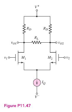
Consider the circuit shown in Figure P11.47. Assume that \(\lambda=0\) for \(M_{1}\) and \(M_{2}\). Also assume an ideal current source \(I_{Q}\). Derive the expression for the one-sided differential mode gains \(A_{d 1}=v_{o 1} / v_{d}\) and \(A_{d 2}=v_{o 2} / v_{d}\), and the two-sided
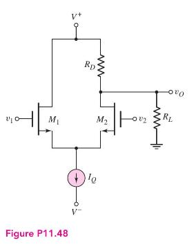
Consider the diff-amp shown in Figure P11.48. Assume \(\lambda_{1}=\lambda_{2}=0\) and assume the current source has an output resistance of \(R_{o}\). (a) Derive the expression for the differential-mode voltage gain \(A_{d}=\Delta v_{O} / v_{d}\) where \(v_{d}=v_{1}-v_{2}\). (b) Derive the
The bias voltages of the diff-amp circuit shown in Figure 11.19 are \(V^{+}=5 \mathrm{~V}\) and \(V^{-}=-5 \mathrm{~V}\), and the bias current is \(I_{Q}=0.2 \mathrm{~mA}\). The transistor parameters are \(V_{T N}=0.4 \mathrm{~V}, K_{n}=0.15 \mathrm{~mA} / \mathrm{V}^{2}\), and \(\lambda=0\). (a)
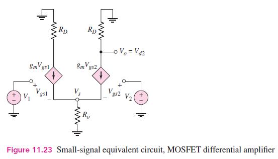
Consider the small-signal equivalent circuit in Figure 11.23. Assume the output is a two-sided output defined as \(V_{o}=V_{d 2}-V_{d 1}\), where \(V_{d 2}\) and \(V_{d 1}\) are the signal voltages at the drains of \(M_{2}\) and \(M_{1}\), respectively. Derive expressions for the differential- and
Consider the MOSFET diff-amp with the configuration in Figure P11.33. The circuit parameters are \(V^{+}=3 \mathrm{~V}, V^{-}=-3 \mathrm{~V}\), and \(I_{Q}=0.2 \mathrm{~mA}\). The transistor parameters are \(V_{T N}=0.4 \mathrm{~V}\), \(k_{n}^{\prime}=100 \mu \mathrm{A} / \mathrm{V}^{2}, W /
Consider the bridge circuit and diff-amp described in Problem 11.27. The BJT diff-amp is to be replaced with a MOSFET diff-amp as shown in Figure 11.19. The transistor parameters are \(V_{T N}=0.4 \mathrm{~V}, K_{n}=1 \mathrm{~mA} / \mathrm{V}^{2}\), and \(\lambda=0\). The bias voltages of the
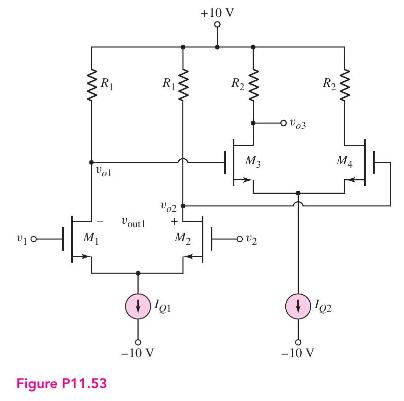
Figure P11.53 shows a two-stage cascade diff-amp with resistive loads. Power supply voltages of \(\pm 10 \mathrm{~V}\) are available. Assume transistor parameters of \(V_{T N}=1 \mathrm{~V}, k_{n}^{\prime}=60 \mu \mathrm{A} / \mathrm{V}^{2}\), and \(\lambda=0\). Design the circuit such that the
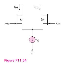
Figure P11.54 shows a matched JFET differential pair biased with a current source \(I_{Q}\). (a) Starting with\[i_{D}=I_{D S S}\left(1-\frac{v_{G S}}{V_{P}}\right)^{2}\]show that\[\frac{i_{D 1}}{I_{Q}}=\frac{1}{2}+\left(\frac{1}{-2 V_{P}}\right) v_{d} \sqrt{2\left(\frac{I_{D S
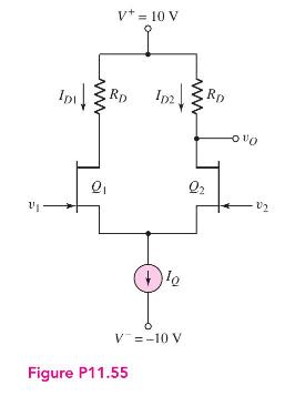
A JFET differential amplifier is shown in Figure P11.55. The transistor parameters are: \(V_{P}=-4 \mathrm{~V}, I_{D S S}=2 \mathrm{~mA}\), and \(\lambda=0\). (a) Find \(R_{D}\) and \(I_{Q}\) such that \(I_{D 1}=I_{D 2}=0.5 \mathrm{~mA}\) and \(v_{o 2}=7 \mathrm{~V}\) when \(v_{1}=v_{2}=0\). (b)
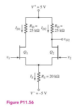
Consider the JFET diff-amp shown in Figure P11.56. The transistor parameters are: \(I_{D S S}=0.8 \mathrm{~mA}, \lambda=0\), and \(V_{P}=-2 \mathrm{~V}\). (a) Determine \(I_{S}\), \(I_{D 1}, I_{D 2}\), and \(v_{o 2}\) for \(v_{1}=v_{2}=0\). (b) Using the small-signal equivalent circuit, determine
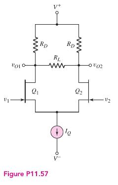
Consider the circuit in Figure P11.57. Assume that \(\lambda=0\) for the transistors, and assume an ideal current source \(I_{Q}\). Derive the expressions for the one-sided differential-mode gains \(A_{d 1}=v_{o 1} / v_{d}\) and \(A_{d 2}=v_{o 2} / v_{d}\), and for the two-sided differential-mode
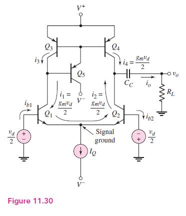
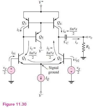
The circuit parameters for the diff-amp shown in Figure 11.30 are \(V^{+}=3.3 \mathrm{~V}, V^{-}=-3.3 \mathrm{~V}\), and \(I_{Q}=0.4 \mathrm{~mA}\). The transistor parameters are \(\beta=120, V_{A 1}=V_{A 2}=120 \mathrm{~V}, V_{A 3}=V_{A 4}=80 \mathrm{~V}\), and \(V_{A 5}=\infty\). (a) Determine
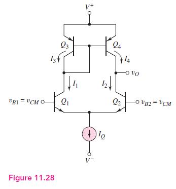
Design a differential amplifier with the configuration shown in Figure 11.28 incorporating a basic two-transistor current source to establish \(I_{Q}\). The bias voltages are to be \(V^{+}=+5 \mathrm{~V}\) and \(V^{-}=-5 \mathrm{~V}\), the bias current is to be \(I_{Q}=250 \mu \mathrm{A}\), and the
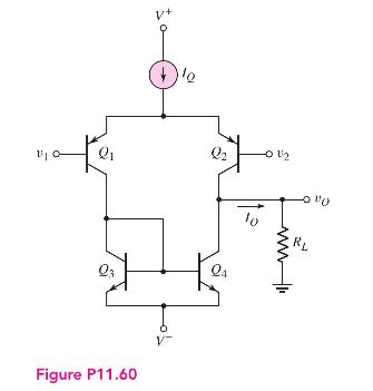
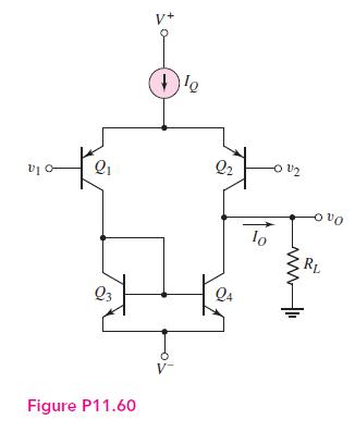
The differential amplifier shown in Figure P11.60 has a pair of pnp bipolars as input devices and a pair of npn bipolars connected as an active load. The circuit bias is \(I_{Q}=0.2 \mathrm{~mA}\), and the transistor parameters are \(\beta=100\) and \(V_{A}=100 \mathrm{~V}\). (a) Determine
The bias voltages for the diff-amp shown in Figure 11.30 are \(V^{+}=5 \mathrm{~V}\) and \(V^{-}=-5 \mathrm{~V}\). A load resistance of \(R_{L}=250 \mathrm{k} \Omega\) is capacitively coupled to the output. The transistor parameters are \(\beta=120\), \(V_{A 1}=V_{A 2}=90 \mathrm{~V}\), and \(V_{A
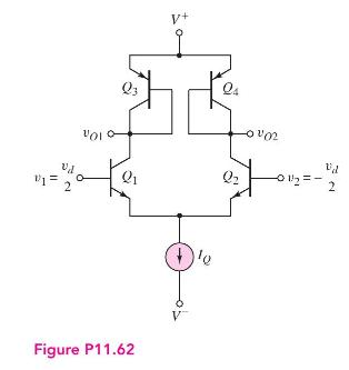
Consider the diff-amp shown in Figure P11.62. The circuit parameters are \(V^{+}=3 \mathrm{~V}, V^{-}=-3 \mathrm{~V}\), and \(I_{Q}=0.4 \mathrm{~mA}\). The npn transistor parameters are \(\beta_{\mathrm{npn}}=180, V_{B E}\) (on) \(=0.7 \mathrm{~V}\), and \(V_{A N}=120 \mathrm{~V}\), and the pnp
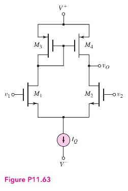
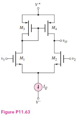
Consider the MOSFET diff-amp shown in Figure P11.63. The bias voltages are \(V^{+}=3 \mathrm{~V}\) and \(V^{-}=-3 \mathrm{~V}\). The current source is \(I_{Q}=200 \mu \mathrm{A}\) and has an output resistance of \(R_{o}=2 \mathrm{M} \Omega\). The transistor parameters are \(V_{T N}=0.4 \mathrm{~V},
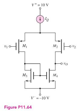
The differential amplifier in Figure P11.64 has a pair of PMOS transistors as input devices and a pair of NMOS transistors connected as an active load. The circuit is biased with \(I_{Q}=0.2 \mathrm{~mA}\), and the transistor parameters are: \(K_{n}=K_{p}=0.1 \mathrm{~mA} / \mathrm{V}^{2}, \quad
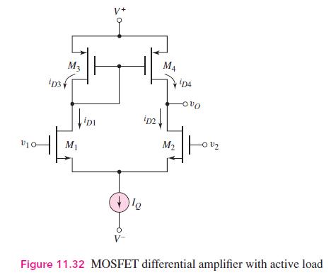
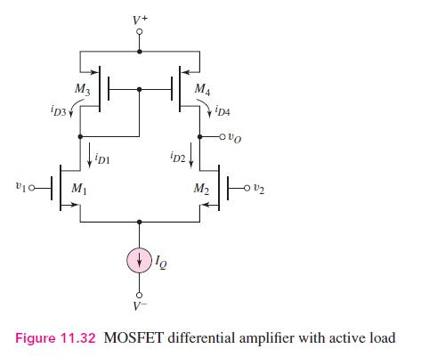
The circuit parameters for the diff-amp shown in Figure 11.32 are \(V^{+}=1.8 \mathrm{~V}, V^{-}=-1.8 \mathrm{~V}\), and \(I_{Q}=120 \mu \mathrm{A}\). The NMOS transistor parameters are \(V_{T N}=0.3 \mathrm{~V}, k_{n}^{\prime}=100 \mu \mathrm{A} / \mathrm{V}^{2},(W / L)_{n}=8\), and
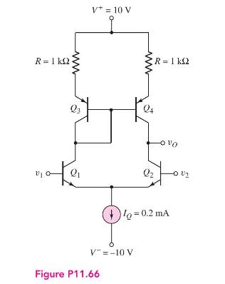
Consider the diff-amp with active load in Figure P11.66. The Early voltages are \(V_{A N}=120 \mathrm{~V}\) for \(Q_{1}\) and \(Q_{2}\) and \(V_{A P}=80 \mathrm{~V}\) for \(Q_{3}\) and \(Q_{4}\). (a) Determine the open-circuit differential-mode voltage gain. (b) Compare this value to the gain
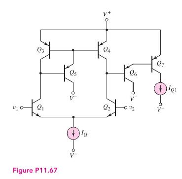
The diff-amp in Figure P11.67 has a three-transistor active load circuit and a Darlington pair configuration connected to the output. Determine the bias current \(I_{Q 1}\) in terms of \(I_{Q}\) such that the diff-amp dc currents are balanced. Q3 1 Figure P11.67 1+ 24 22 26 101
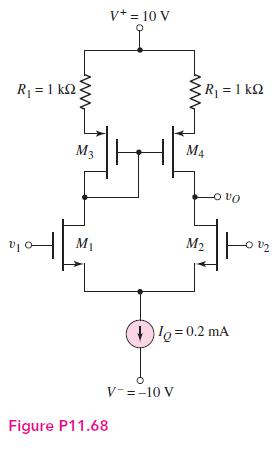
Consider the diff-amp in Figure P11.68. The PMOS parameters are: \(K_{p}=\) \(80 \mu \mathrm{A} / \mathrm{V}^{2}, \lambda_{p}=0.02 \mathrm{~V}^{-1}, V_{T P}=-2 \mathrm{~V}\). The NMOS parameters are: \(K_{n}=80 \mu \mathrm{A} / \mathrm{V}^{2}, \lambda_{n}=0.015 \mathrm{~V}^{-1}, V_{T N}=+2
Reconsider the circuit in Figure P11.60 except that \(1 \mathrm{k} \Omega\) resistors are inserted at the emitters of the active load transistors \(Q_{3}\) and \(Q_{4}\) as in the circuit in Figure P11.66. Assume the same transistor parameters as in Problem 11.60. (a) Determine the output
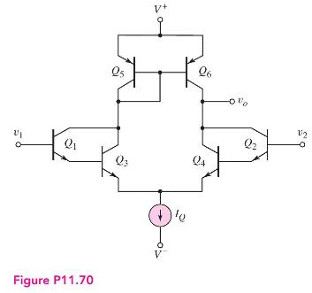
Consider the circuit in Figure P11.70, in which the input transistors to the diff-amp are Darlington pairs. Assume transistor parameters of \(\beta(\mathrm{npn})=120, \beta(\mathrm{pnp})=80, V_{A}(\mathrm{npn})=100 \mathrm{~V}\), and \(V_{A}(\mathrm{pnp})=80 \mathrm{~V}\). Let the power supply
Design a BJT diff-amp with an active load similar to the configuration in Figure P11.70 except that the input devices are to be pnp transistors and the active load will have npn transistors. Using the same parameters as in Problem 11.70, determine the small-signal differential-mode voltage
Reconsider the diff-amp specifications listed in Problem 11.45. Design an all-CMOS diff-amp with the configuration in Figure 11.32 to meet the specifications. The NMOS transistor parameters are \(V_{T N}=0.4 \mathrm{~V}\), \(k_{n}^{\prime}=100 \mu \mathrm{A} / \mathrm{V}^{2}\), and
An all-CMOS diff-amp, including the current source circuit, with the configuration in Figure 11.32 is to be designed to have a differential-mode gain of \(A_{d}=240\). The bias voltages are \(V^{+}=3 \mathrm{~V}\) and \(V^{-}=-3 \mathrm{~V}\). The total power dissipation in the circuit is to be
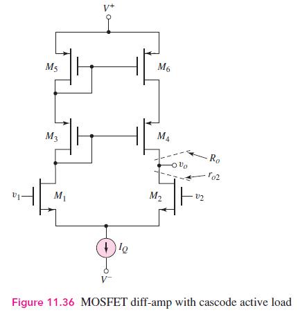
The differential amplifier with the configuration shown in Figure 11.36 is to be designed to achieve a differential-mode voltage gain of \(A_{d}=400\). The circuit parameters are to be \(V^{+}=+5 \mathrm{~V}, V^{-}=-5 \mathrm{~V}\), and \(I_{Q}=200 \mu \mathrm{A}\). The available transistors have
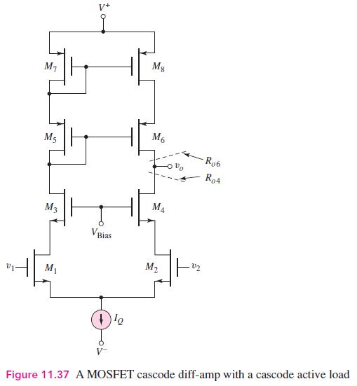
Consider the fully cascoded diff-amp in Figure 11.37. Assume \(I_{Q}=80 \mu \mathrm{A}\) and transistor parameters of: \(V_{T N}=0.8 \mathrm{~V}, k_{n}^{\prime}=60 \mu \mathrm{A} / \mathrm{V}^{2}\), \(\lambda_{n}=0.015 \mathrm{~V}^{-1}, V_{T P}=-0.8 \mathrm{~V}, k_{p}^{\prime}=25 \mu \mathrm{A} /
Consider the diff-amp that was shown in Figure P11.63. The circuit and transistor parameters are \(V^{+}=2.8 \mathrm{~V}, V^{-}=-2.8 \mathrm{~V}, I_{Q}=120 \mu \mathrm{A}\), \(K_{n}=K_{p}=0.2 \mathrm{~mA} / \mathrm{V}^{2}, V_{T N}=+0.3 \mathrm{~V}, V_{T P}=-0.3 \mathrm{~V}\), and
The diff-amp in Figure P11.63 is biased at \(I_{Q}=0.5 \mathrm{~mA}\). The transistor parameters are \(K_{n}=K_{p}=0.25 \mathrm{~mA} / \mathrm{V}^{2}, V_{T N}=0.4 \mathrm{~V}, V_{T P}=-0.4 \mathrm{~V}\), and \(\lambda_{n}=\lambda_{p}=0.02 \mathrm{~V}^{-1}\). (a) What are the minimum power supply
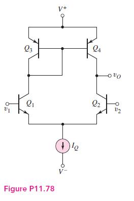
The circuit and transistor parameters of the bipolar diff-amp shown in Figure P11.78 are \(I_{Q}=200 \mu \mathrm{A}, \beta_{\text {npn }}=125, \beta_{\text {pnp }}=80, V_{B E}(\) on \()=\) \(V_{E B}(\) on \()=0.7 \mathrm{~V}, V_{A N}=100 \mathrm{~V}\), and \(V_{A P}=60 \mathrm{~V}\). (a) What are
Repeat Problem 11.78 if \(I_{Q}=120 \mu \mathrm{A}, V_{A N}=75 \mathrm{~V}\), and \(V_{A P}=40 \mathrm{~V}\). All other parameters remain the same.Data From Problem 11.78:-The circuit and transistor parameters of the bipolar diff-amp shown in Figure P11.78 are \(I_{Q}=200 \mu \mathrm{A},
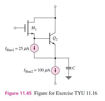
(a) The Darlington pair circuit in Figure 11.45 has new bias current levels of \(I_{\text {BIAS } 1}=0.25 \mathrm{~mA}\) and \(I_{\text {BIAS } 2}=0.50 \mathrm{~mA}\). The transistor parameters are \(K_{n}=0.2 \mathrm{~mA} / \mathrm{V}^{2}, V_{T N}=0.4 \mathrm{~V}\), and \(\lambda=0\) for \(M_{1}
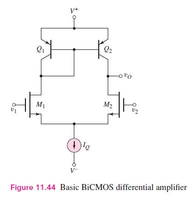
Consider the BiCMOS diff-amp in Figure 11.44, biased at \(I_{Q}=0.4 \mathrm{~mA}\). The transistor parameters for \(M_{1}\) and \(M_{2}\) are: \(K_{n}=0.2 \mathrm{~mA} / \mathrm{V}^{2}, V_{T N}=1\) \(\mathrm{V}\), and \(\lambda=0.01 \mathrm{~V}^{-1}\). The parameters for \(Q_{1}\) and \(Q_{2}\)
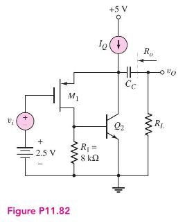
The BiCMOS circuit shown in Figure P11.82 is equivalent to a pnp bipolar transistor with an infinite input impedance. The bias current is \(I_{Q}=0.5 \mathrm{~mA}\). The MOS transistor parameters are \(V_{T P}=-0.5 \mathrm{~V}, K_{p}=0.7 \mathrm{~mA} / \mathrm{V}^{2}\), and \(\lambda=0\), and the
The bias current in the BiCMOS circuit shown in Figure P11.82 is \(I_{Q}=0.8 \mathrm{~mA}\). The transistor parameters are the same as described in Problem 11.82. (a) Sketch the small-signal equivalent circuit and calculate the small-signal parameters for each transistor. (b) Determine the output
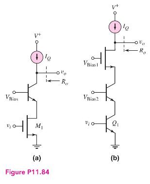
The bias current \(I_{Q}\) is \(25 \mu \mathrm{A}\) in each circuit in Figure P11.84. The BJT parameters are \(\beta=100\) and \(V_{A}=50 \mathrm{~V}\), and the MOSFET parameters are \(V_{T N}=0.8 \mathrm{~V}, K_{n}=0.25 \mathrm{~mA} / \mathrm{V}^{2}\), and \(\lambda=0.02 \mathrm{~V}^{-1}\). Assume
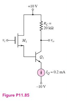
For the circuit shown in Figure P11.85, determine the small-signal voltage gain, \(A_{v}=v_{o} / v_{i}\). Assume transistor parameters of \(V_{T N}=1 \mathrm{~V}, K_{n}=\) \(0.2 \mathrm{~mA} / \mathrm{V}^{2}\), and \(\lambda=0\) for \(M_{1}\) and \(\beta=80\) and \(V_{A}=\infty\) for \(Q_{1}\). 1
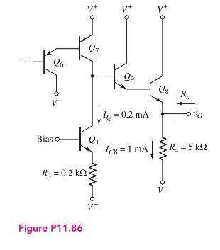
The output stage in the circuit shown in Figure P11.86 is a Darlington pair emitter-follower configuration. Assume \(\beta=120\) for all npn transistors and \(\beta=90\) for all pnp transistors. Let \(V_{A 7}=60 \mathrm{~V}\) for \(Q_{7}, V_{A 11}=120 \mathrm{~V}\) for \(Q_{11}\), and
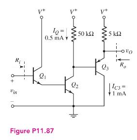
For the circuit in Figure P11.87, the transistor parameters are \(\beta=100\) and \(V_{A}=\infty\). The bias currents in the transistors are indicated on the figure. Determine the input resistance \(R_{i}\), the output resistance \(R_{o}\), and the smallsignal voltage gain \(A_{v}=v_{o} / v_{i
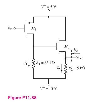
Consider the circuit in Figure P11.88. The bias currents \(I_{1}\) and \(I_{2}\) are such that a zero dc output voltage is established. The transistor parameters are: \(K_{p}=0.2 \mathrm{~mA} / \mathrm{V}^{2}, K_{n}=0.5 \mathrm{~mA} / \mathrm{V}^{2}, V_{T P}=-0.8 \mathrm{~V}, V_{T N}=+0.8
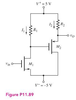
The bias currents in the circuit shown in Figure P11.89 are \(I_{1}=0.25 \mathrm{~mA}\) and \(I_{2}=1.0 \mathrm{~mA}\). The transistor parameters are \(K_{n}=0.5 \mathrm{~mA} / \mathrm{V}^{2}\), \(K_{p}=1.0 \mathrm{~mA} / \mathrm{V}^{2}, V_{T N}=0.8 \mathrm{~V}, V_{T P}=-0.8 \mathrm{~V}\), and
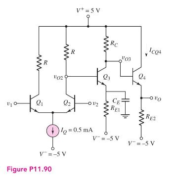
Consider the multistage bipolar circuit in Figure P11.90, in which dc base currents are negligible. Assume the transistor parameters are \(\beta=120\), \(V_{B E}\) (on) \(=0.7 \mathrm{~V}\), and \(V_{A}=\infty\). The output resistance of the constant current source is \(R_{o}=200 \mathrm{k}
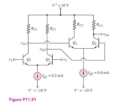
The circuit in Figure P11.91 has two bipolar differential amplifiers in cascade, biased with ideal current sources \(I_{Q 1}\) and \(I_{Q 2}\). Assume the transistor parameters are \(\beta=180\) and \(V_{A}=\infty\). (a) Design the circuit such that \(v_{o 1}=v_{o 2}=2 \mathrm{~V}\) and \(v_{O 4}=6
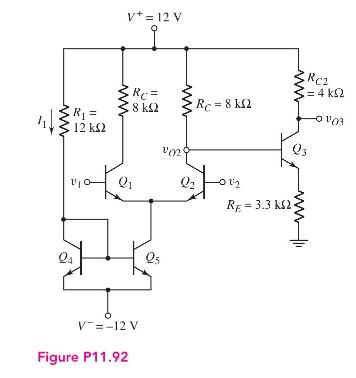
The transistor parameters for the circuit in Figure P11.92 are: \(\beta=200\), \(V_{B E}(\mathrm{on})=0.7 \mathrm{~V}\), and \(V_{A}=80 \mathrm{~V}\). (a) Determine the differential-mode voltage gain \(A_{d}=v_{o 3} / v_{d}\) and the common-mode voltage gain \(A_{c m}=\) \(v_{o 3} / v_{c m}\). (b)
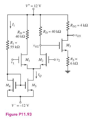
For the transistors in the circuit in Figure P11.93, the parameters are: \(K_{n}=0.2 \mathrm{~mA} / \mathrm{V}^{2}, V_{T N}=2 \mathrm{~V}\), and \(\lambda=0.02 \mathrm{~V}^{-1}\). (a) Determine the differential-mode voltage gain \(A_{d}=v_{o 3} / v_{d}\) and the common-mode voltage gain \(A_{c
Consider the differential amplifier in Figure 11.50(a) with parameters \(I_{Q}=0.8 \mathrm{~mA}, R_{C}=10 \mathrm{k} \Omega\), and \(R_{B}=0.5 \mathrm{k} \Omega\). The transistor parameters are \(\beta=150, V_{B E}\) (on) \(=0.7 \mathrm{~V}, V_{A}=\infty, C_{\pi}=1.2 \mathrm{pF}\), and
The differential amplifier in Figure 11.51 (a) has the same circuit and transistor parameters as described in Problem 11.94. The equivalent impedance of the current source is \(R_{o}=10 \mathrm{M} \Omega\) and \(C_{o}=0.4 \mathrm{pF}\).(a) Determine the frequency of the zero in the common-mode
A BJT diff-amp is biased with a current source \(I_{Q}=2 \mathrm{~mA}\), and the circuit parameters are \(R_{C}=10 \mathrm{k} \Omega\) and \(R_{B}=1 \mathrm{k} \Omega\). The transistor parameters are: \(\beta=120, f_{T}=800 \mathrm{MHz}\), and \(C_{\mu}=1 \mathrm{pF}\). (a) Determine the upper \(3
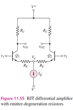
Consider the diff-amp in Figure 11.55. The circuit and transistor parameters are the same as in Problem 11.6. For a one-sided output at \(v_{o 2}\), determine the differential-mode gain for: (a) \(R_{E}=100 \Omega\), and (b) \(R_{E}=250 \Omega\). V+ www RC RC www 102 Q2 Ve RE RE Figure 11.55 BJT
Using a computer simulation, verify the results of Example 11.12.Data From Example 11.12:-Data From Example 11.11:-Data From Example 11.4:-Figure 11.32:-Figure 11.36:- Calculate the differential-mode voltage gain of a MOSFET diff-amp with a cascode active load. Consider the diff-amp shown in Figure
Using a computer simulation, verify the results of Example 11.13 for the simple op-amp circuit.Data From Example 11.13:- Calculate the input resistance and the small-signal voltage gain of a Darlington pair.
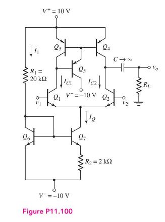
Consider the circuit in Figure P11.100. Use standard transistors. Using a computer simulation, determine the small-signal differential-mode voltage gain and common-mode voltage gain for (a) \(R_{L}=10 \mathrm{M} \Omega\) and (b) \(R_{L}=200 \mathrm{k} \Omega\). V*= 10 V R = 20 k2 Q3 Q Q5 V-=-10 V
Showing 600 - 700
of 4723
1
2
3
4
5
6
7
8
9
10
11
12
13
14
15
Last
Step by Step Answers