New Semester
Started
Get
50% OFF
Study Help!
--h --m --s
Claim Now
Question Answers
Textbooks
Find textbooks, questions and answers
Oops, something went wrong!
Change your search query and then try again
S
Books
FREE
Study Help
Expert Questions
Accounting
General Management
Mathematics
Finance
Organizational Behaviour
Law
Physics
Operating System
Management Leadership
Sociology
Programming
Marketing
Database
Computer Network
Economics
Textbooks Solutions
Accounting
Managerial Accounting
Management Leadership
Cost Accounting
Statistics
Business Law
Corporate Finance
Finance
Economics
Auditing
Tutors
Online Tutors
Find a Tutor
Hire a Tutor
Become a Tutor
AI Tutor
AI Study Planner
NEW
Sell Books
Search
Search
Sign In
Register
study help
computer science
systems analysis and design 12th
Microelectronics Circuit Analysis And Design 4th Edition Donald A. Neamen - Solutions
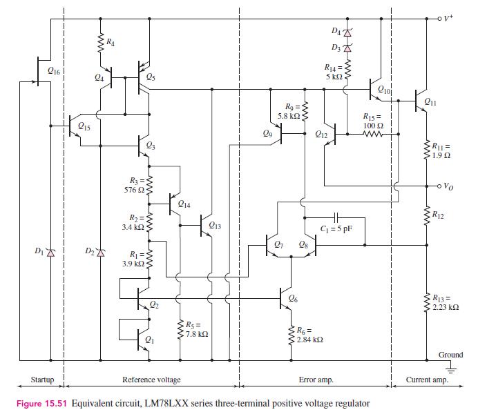
Consider the three-terminal voltage regulator in Figure 15.51, with Zener diode voltages of \(V_{Z}=6.3 \mathrm{~V}\). Assume transistor parameters of \(V_{B E}(\mathrm{npn})=\) \(V_{E B}(\mathrm{pnp})=0.6 \mathrm{~V}\), and neglect base currents. (a) Determine resistance \(R_{4}\) such that \(I_{Z
The three-terminal voltage regulator in Figure 15.51 has parameters as described in Example 15.16. Assume \(R_{4}=0, V_{A}=50 \mathrm{~V}\) for \(Q_{4}\), and \(r_{z}=15 \Omega\) for \(D_{2}\). Determine the line regulation.Data From Example 15.16:-Figure 15.51:- Determine the bias current,
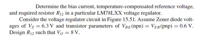
The voltage regulator shown in Figure P15.79 is a variable voltage, 0 to \(5 \mathrm{~A}\) power supply. The transistor parameters are \(\beta=80\) and \(V_{B E}(\mathrm{on})=0.7 \mathrm{~V}\). The op-amp has a finite open-loop gain of \(A_{O L}=5 \times 10^{3}\). The zero-current Zener voltage is
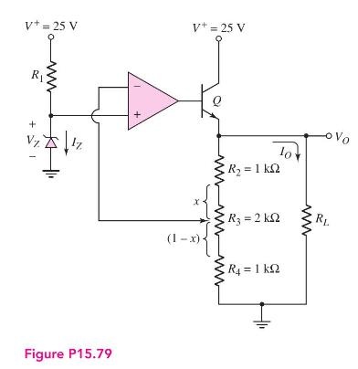
The parameters of the transistor in Figure \(\mathrm{P} 15.80\) are \(\beta=80\) and \(V_{E B}\) (on) \(=0.6 \mathrm{~V}\). The Zener diode is ideal with \(V_{Z}=6.8 \mathrm{~V}\) and the op-amp is ideal. (a) Determine the range of load resistance \(R_{L}\) such that the load current is a constant.
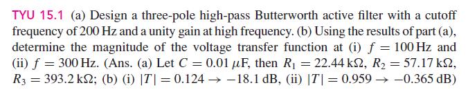
Consider the three-pole high-pass Butterworth active filter described in Exercise TYU 15.1. Using a computer simulation, plot the magnitude of the voltage transfer function versus frequency and compare these results with those obtained in TYU 15.1.Data From Exercise TYU 15.1:- TYU 15.1 (a) Design a
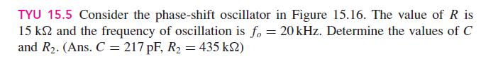
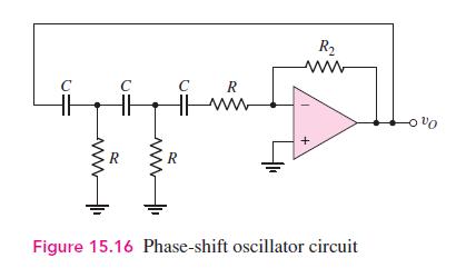
A phase shift oscillator is described in Exercise TYU 15.5. Using a computer simulation, plot the output voltage of the oscillator versus time over several cycles. What is the frequency of oscillation?Data From Exercise TYU 15.5:- TYU 15.5 Consider the phase-shift oscillator in Figure 15.16. The
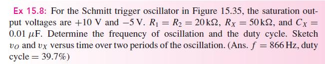
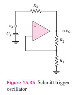
Consider the Schmitt trigger oscillator described in Exercise Ex 15.8. Using a computer simulation, plot the voltage \(v_{X}\) versus time over several cycles. What is the frequency of oscillation?Data From Exercise Ex 15.8:- Ex 15.8: For the Schmitt trigger oscillator in Figure 15.35, the
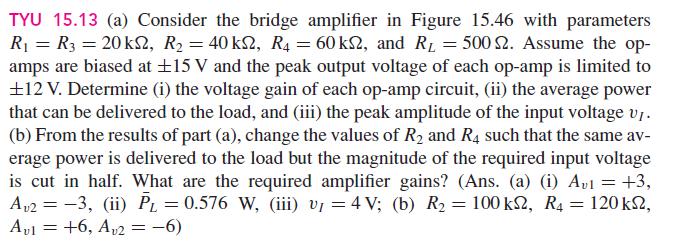
A bridge power amplifier is described in Exercise TYU 15.13. Using a computer simulation, plot (a) \(v_{O 1}-v_{O 2}\) versus \(v_{I}\) over the range \(0 \leq v_{I} \leq 4 \mathrm{~V}\) and (b) the current in \(R_{L}\) over the same input voltage range.Data From Exercise TYU 15.13:- TYU 15.13 (a)
Design a four-pole high-pass Butterworth active filter such that the lowfrequency voltage gain is +20 and the cutoff frequency is \(50 \mathrm{~Hz}\).
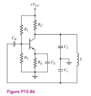
Consider the Colpitts oscillator in Figure P15.86. The capacitors \(C_{E}\) and \(C_{B}\) are very large bypass and coupling capacitors. Let \(V_{C C}=5 \mathrm{~V}\). (a) Design the circuit such that the quiescent collector current is \(I_{C Q}=0.5 \mathrm{~mA}\). (b) Design the circuit such that
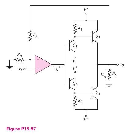
Consider the power amplifier in Figure P15.87 with parameters \(V^{+}=15 \mathrm{~V}, V^{-}=-15 \mathrm{~V}\), and \(R_{L}=20 \Omega\). The closed-loop gain must be 10. Design the circuit such that the power delivered to the load is \(5 \mathrm{~W}\) when \(v_{I}=-1 \mathrm{~V}\). If the four
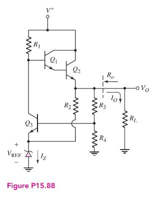
Consider the simple series-pass regulator circuit in Figure P15.88. Assume an ideal Zener diode with \(V_{Z}=V_{\mathrm{REF}}=4.7 \mathrm{~V}\). Let \(\beta=100\) and \(V_{B E}(\) on \()=0.7 \mathrm{~V}\) for all transistors. (a) Design the circuit such that \(V_{O}=10 \mathrm{~V}\) and \(I_{Z}=10
Sketch the quasi-static voltage transfer characteristics of an NMOS inverter with depletion load. What effect does changing the transistor \(W / L\) ratio have on the transfer characteristics?
Sketch an NMOS three-input NOR logic gate. Describe its operation. Discuss the condition under which the maximum logic 0 value is obtained.
Discuss how more sophisticated (compared to the basic NOR and NAND) logic functions can be implemented in a single NMOS logic circuit.
Sketch the quasi-static voltage transfer characteristics of a CMOS inverter. Discuss the various intervals in terms of transistor bias. What is the effect on the transfer curve of changing the transistor \(W / L\) ratios? What is the advantage of the CMOS inverter compared to an NMOS inverter?
Discuss the parameters that affect the switching power dissipation in a CMOS inverter.
Define the noise margin in a CMOS inverter.
Sketch a CMOS three-input NAND logic gate. Describe its operation. Determine the relative transistor \(W / L\) ratios to obtain equal pull-up and pull-down switching times.
Discuss how more sophisticated (compared to the basic NOR and NAND) logic functions can be implemented in a single CMOS logic circuit.
Discuss the basic principles of a clocked CMOS logic circuit.
Sketch an NMOS transmission gate and describe its operation. What is the maximum output voltage?
Sketch a CMOS transmission gate and describe its operation. Why is the quasistatic output voltage always equal to the quasi-static input voltage?
Discuss what is meant by pass transistor logic.
If an NMOS or CMOS transmission gate is turned off (an open switch), discuss why the output voltage is, in general, not stable.
Sketch an NMOS dynamic shift register and describe its operation.
Sketch a CMOS R-S flip flop and describe its operation. Why must the input condition \(R=S=1\) be avoided?
Describe the basic architecture of a semiconductor random-access memory.
Sketch a CMOS SRAM cell and describe its operation. Discuss any advantages and disadvantages of this design. Describe how the cell is addressed.
Sketch a one-transistor DRAM cell and describe its operation. What makes this circuit dynamic?
Describe a mask-programmed MOSFET ROM memory.
Describe the basic operation of a floating gate MOSFET and how this can be used in an erasable ROM.
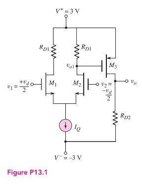
Consider the simple MOS op-amp circuit shown in Figure P13.1. The bias current is \(I_{Q}=200 \mu \mathrm{A}\). Transistor parameters are \(k_{n}^{\prime}=100 \mu \mathrm{A} / \mathrm{V}^{2}, k_{p}^{\prime}=\) \(40 \mu \mathrm{A} / \mathrm{V}^{2}, V_{T N}=0.4 \mathrm{~V}, V_{T P}=-0.4
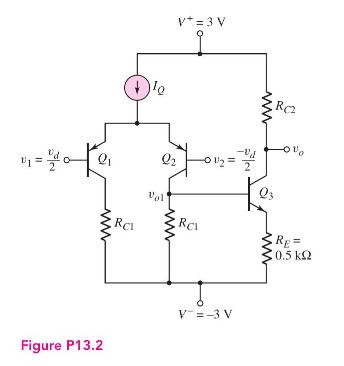
Consider the simple bipolar op-amp circuit shown in Figure P13.2. The bias current is \(I_{Q}=0.5 \mathrm{~mA}\). Transistor parameters are \(\beta_{n}=180, \beta_{p}=120\), \(V_{B E}\) (on) \(=V_{E B}\) (on) \(=0.7 \mathrm{~V}\), and \(V_{A n}=V_{A p}=\infty\). (a) Design the circuit such that
Design the circuit in Figure 13.2 such that the maximum power dissipated in the circuit is \(15 \mathrm{~mW}\) and such that the common-mode input voltage is in the range \(-3 \leq v_{C M} \leq 3 \mathrm{~V}\). Using a computer simulation, adjust the value of \(R_{3}\) such that the output
Using the results of Problem 13.3, determine, from a computer simulation, the differential-mode voltage gain of the diff-amp and the voltage gain of the second stage of the op-amp circuit in Figure 13.2. Use standard transistor models in the circuit.Data From Problem 13.3:-Design the circuit in
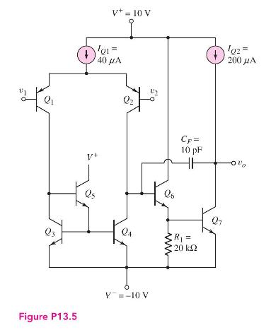
Consider the BJT op-amp circuit in Figure P13.5. The transistor parameters are: \(\beta(\mathrm{npn})=120, \beta(\mathrm{pnp})=80, V_{A}=80 \mathrm{~V}\) (all transistors), and baseemitter turn-on voltage \(=0.6 \mathrm{~V}\) (all transistors). (a) Determine the smallsignal differential-mode
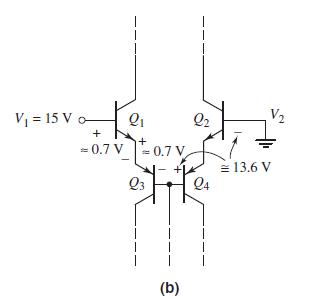
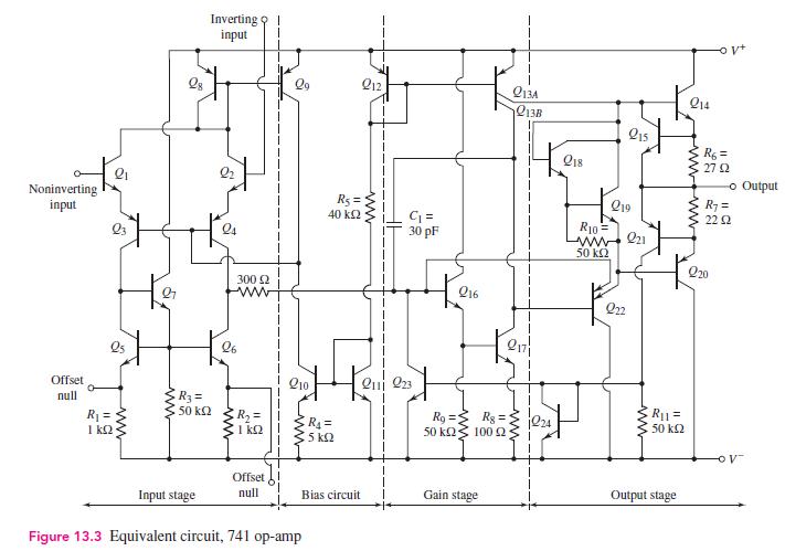
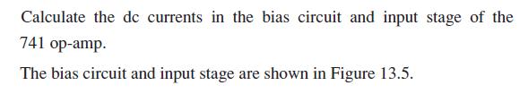
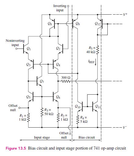
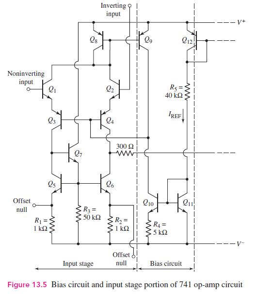
Consider the input stage of the 741 op-amp in Figure 13.4(b).(a) Assume the input voltages are \(V_{1}=0\) and \(V_{2}=+15 \mathrm{~V}\). Consider the B-E voltage of each transistor and determine which transistor acts as the protection device.(b) Repeat part (a) for \(V_{1}=-15 \mathrm{~V}\) and
For the input stage of the 741 op-amp, assume B-E breakdown voltages of \(5 \mathrm{~V}\) for the npn devices and \(50 \mathrm{~V}\) for the pnp devices. Estimate the differential input voltage at which breakdown will occur.
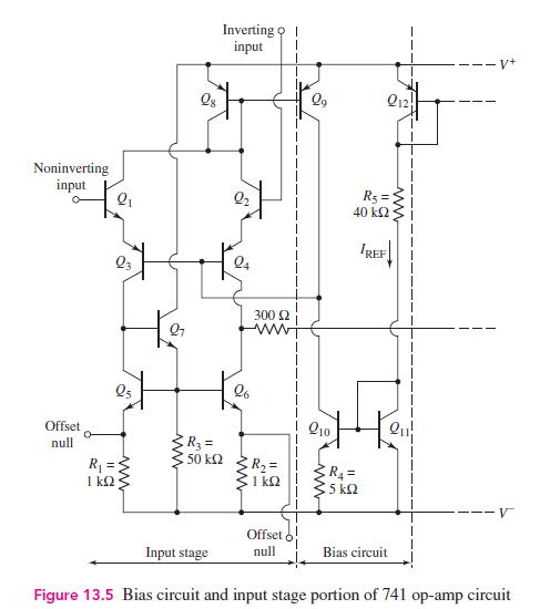
Consider the bias circuit portion of the 741 op-amp in Figure 13.5. Assume transistor parameters of \(I_{S}=5 \times 10^{-16} \mathrm{~A}\). Neglect base currents.(a) Redesign the circuit such that \(I_{\mathrm{REF}}=0.5 \mathrm{~mA}\) and \(I_{C 10}=30 \mu \mathrm{A}\) for bias voltages of \(\pm
Repeat Problem 13.8 for bias voltages of \(\pm 5 \mathrm{~V}\).Data From Problem 13.8:-Consider the bias circuit portion of the 741 op-amp in Figure 13.5. Assume transistor parameters of \(I_{S}=5 \times 10^{-16} \mathrm{~A}\). Neglect base currents.(a) Redesign the circuit such that
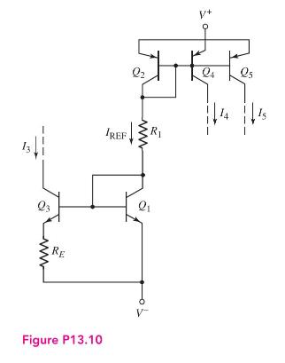
Consider the bias circuit shown in Figure P13.10. Let \(V^{+}=3 \mathrm{~V}\), \(V^{-}=-3 \mathrm{~V}, R_{1}=80 \mathrm{k} \Omega\), and \(R_{E}=3.5 \mathrm{k} \Omega\). Assume transistor parameters of \(I_{S}=5 \times 10^{-15} \mathrm{~A}\) for \(Q_{1}, Q_{2}, Q_{3} ; I_{S}=3 \times 10^{-15}
The minimum recommended supply voltages for the 741 op-amp are \(V^{+}=5 \mathrm{~V}\) and \(V^{-}=-5 \mathrm{~V}\). Using these lower supply voltages, calculate: \(I_{\mathrm{REF}}, I_{C 10}, I_{C 6}, I_{C 17}\), and \(I_{C 13 A}\).
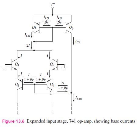
An expanded circuit diagram of the 741 input stage is shown in Figure 13.6. Assume \(I_{C 10}=50 \mu \mathrm{A}\). If the current gain of the npn transistors is \(\beta_{n}=90\) and the current gain of the pnp transistors is \(\beta_{p}=40\), determine \(I_{C 9}, I_{C 2}\), \(I_{C 4}, I_{B 9}\),
Consider the 741 op-amp in Figure 13.3, biased with \(V^{+}=15 \mathrm{~V}\) and \(V^{-}=-15 \mathrm{~V}\). Assume that no load is connected at the output, and let the input voltages be zero. Calculate the total power dissipated in the op-amp circuit. What are the currents supplied by \(V^{+}\)and
Consider the 741 circuit in Figure 13.3.(a) Determine the maximum range of common-mode input voltage if the bias voltages are \(\pm 15 \mathrm{~V}\).(b) Repeat part (a) if the bias voltages are \(\pm 5 \mathrm{~V}\). Noninverting input Offset null R = 1 www www Q8 R3 = 50 Inverting input 212 Q13A
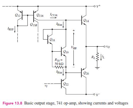
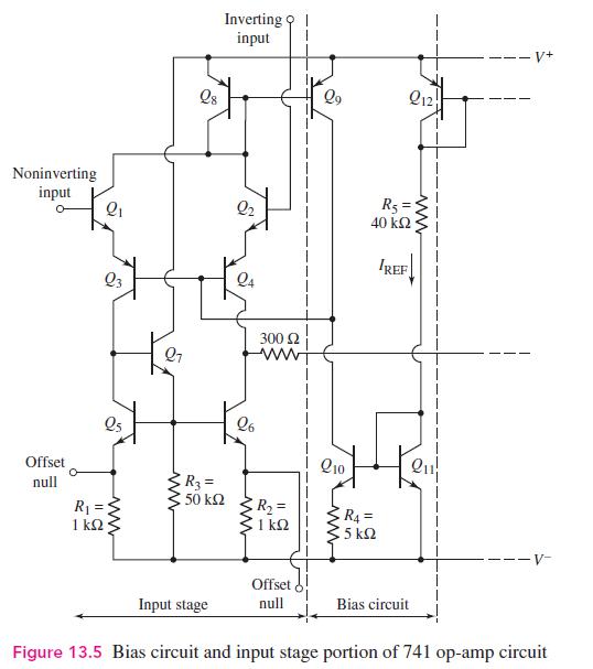
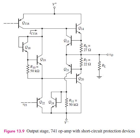
Consider the output stage of the 741 op-amp shown in Figure 13.8. Assume \(v_{1}=v_{2}=0\) at the input and assume the bias voltages are \(V^{+}=5 \mathrm{~V}\) and \(V^{-}=-5 \mathrm{~V}\). Let \(I_{\text {REF }}=0.5 \mathrm{~mA}\). All other circuit and transistor parameters are described in
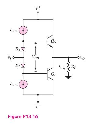
Consider the output stage in Figure P13.16 with parameters \(V^{+}=5 \mathrm{~V}\), \(V^{-}=-5 \mathrm{~V}, R_{L}=10 \mathrm{k} \Omega\), and \(I_{\text {Bias }}=80 \mu \mathrm{A}\). Assume the diode parameters are \(I_{S D}=5 \times 10^{-15} \mathrm{~A}\), and assume the transistor parameters are
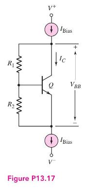
Figure P13.17 shows a circuit often used to provide the \(V_{B B}\) voltage in the op-amp output stage. Assume \(I_{S}=5 \times 10^{-15} \mathrm{~A}\) for the transistor, \(I_{\text {Bias }}=\) \(120 \mu \mathrm{A}\), and \(I_{C}=0.9 I_{\text {Bias }}\). Neglect the base current. Design the circuit
Assume bias voltages on the 741 op-amp of \(\pm 15 \mathrm{~V}\). (a) Determine the differential-mode voltage gain of the first stage if \(R_{1}=R_{2}=0\). (b) Determine the voltage gain of the second stage if \(R_{8}=0\).
Recalculate the voltage gain of the \(741 \mathrm{op}-\mathrm{amp}\) input stage if \(I_{C 10}=40 \mu \mathrm{A}\).
Assume the 741 op-amp shown in Figure 13.3 is biased at \(\pm 5 \mathrm{~V}\). Using the circuit parameters given in the figure and transistor parameters given in Examples 13.1, calculate the overall small-signal voltage gain of the amplifier.Data From Example 13.1:- Calculate the dc currents in
Repeat Problem 13.20 assuming Early voltages of \(100 \mathrm{~V}\).Data From Problem 13.20:-Assume the 741 op-amp shown in Figure 13.3 is biased at \(\pm 5 \mathrm{~V}\). Using the circuit parameters given in the figure and transistor parameters given in Examples 13.1, calculate the overall
Consider the output stage of the 741 op-amp shown in Figure 13.8. Assume \(I_{\text {Bias }}=0.18 \mathrm{~mA}\) and assume transistor parameters of \(I_{S}=10^{-14} \mathrm{~A}\) and \(\beta_{n}=200\). (a) Determine the value of \(R_{10}\) that would result in \(I_{C 18}=\) \(0.25 I_{C 19}\). (b)
The basic bias circuit of the output transistors of the 741 op-amp is shown in Figure P13.23. (a) Sketch the small-signal equivalent circuit. (b) Assuming \(V_{A}=50 \mathrm{~V}\) and using the parameters described in Example 13.3, determine the equivalent small-signal resistance \(R_{e q}=v_{x} /
Calculate the output resistance of the \(741 \mathrm{op-amp}\) if \(Q_{14}\) is conducting and \(Q_{20}\) is cut off. Assume an output current of \(2 \mathrm{~mA}\).
(a) Determine the differential input resistance of the \(741 \mathrm{op}\)-amp when biased at \(\pm 15 \mathrm{~V}\).(b) Repeat part (a) when the op-amp is biased at \(\pm 5 \mathrm{~V}\).
The frequency response of a particular 741 op-amp shows that the opamp has a phase margin of 70 degrees. If a second single pole exists, in addition to the dominant pole, determine the frequency of the second pole. Use the overall gain and dominant-pole parameters calculated in Section 13.2.
An op-amp that is internally compensated by Miller compensation has a unity-gain bandwidth of \(10 \mathrm{MHz}\) and a low-frequency gain of \(10^{6}\). (a) What is the dominant pole frequency? (b) The feedback capacitor is across the second stage, which has a gain of \(-10^{3}\). The effective
A three-stage 741 op-amp has a low-frequency open-loop gain of 200,000 and a dominant pole frequency of \(10 \mathrm{~Hz}\). The second and third poles are at the same frequency. If the phase margin is 70 degrees, determine the frequency of the second and third poles.
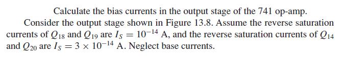
Consider the simple CMOS op-amp circuit in Figure P13.29 biased with \(I_{Q}=200 \mu \mathrm{A}\). The transistor parameters are \(k_{n}^{\prime}=100 \mu \mathrm{A} / \mathrm{V}^{2}, k_{p}^{\prime}=\) \(40 \mu \mathrm{A} / \mathrm{V}^{2}, V_{T N}=0.4 \mathrm{~V}, V_{T P}=-0.4 \mathrm{~V}\), and
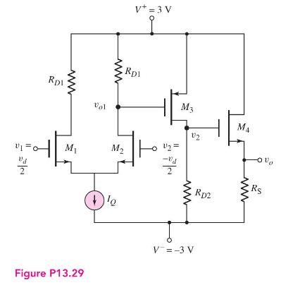
A simple CMOS op-amp circuit is shown in Figure P13.30 with \(I_{Q}=\) \(100 \mu \mathrm{A}\). The transistor parameters are the same as given in Problem 13.29 except for the width-to-length ratios. The width-to-length ratios are \((W / L)_{1,2}=80,(W / L)_{3}=25\), and \((W / L)_{4}=100\). (a) The
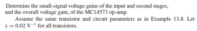
Consider the MC14573 op-amp in Figure 13.14. The dc bias currents and small-signal voltage gains were determined in Examples 13.8 and 13.9. Redesign the circuit such that the width-to-length ratio of \(M_{1}\) and \(M_{2}\) is increased from 12.5 to 50 . All other circuit and transistor parameters
Consider the basic diff-amp with active load and current biasing in Figure 13.14. Using the parameters and results of Example 13.8, determine the maximum range of common-mode input voltage under the conditions that the minimum source-to-drain voltage for a PMOS is limited to \(v_{S
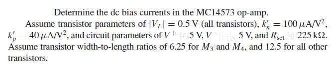
The CMOS op-amp in Figure 13.14 is biased at \(V^{+}=5 \mathrm{~V}\) and \(V^{-}=\) \(-5 \mathrm{~V}\). Let \(R_{\mathrm{set}}=50 \mathrm{k} \Omega\). Assume transistor parameters of \(V_{T N}=0.7 \mathrm{~V}\), \(V_{T P}=-0.7 \mathrm{~V}, k_{n}^{\prime}=100 \mu \mathrm{A} / \mathrm{V}^{2},
For the CMOS op-amp in Figure 13.14, the dc biasing is designed such that \(I_{\text {set }}=I_{Q}=I_{D Q 8}=200 \mu \mathrm{A}\). The transistor parameters are \(V_{T N}=0.5 \mathrm{~V}\), \(V_{T P}=-0.5 \mathrm{~V}, k_{n}^{\prime}=100 \mu \mathrm{A} / \mathrm{V}^{2}, k_{p}^{\prime}=40 \mu
Consider the MC14573 op-amp in Figure 13.14, with circuit and transistor parameters as given in Examples 13.8 and 13.9. If the compensation capacitor is \(C_{1}=12 \mathrm{pF}\), determine the dominant-pole frequency.Data From Example 13.8:-Data From Example 13.9:- Determine the dc bias currents in
The CMOS op-amp in Figure 13.14 has circuit and transistor parameters as given in Problem 13.33. Determine the compensation capacitor required such that the dominant-pole frequency is \(f_{P D}=8 \mathrm{~Hz}\). V+ Mg M6 M5 Iset www M M2 C Ovo Rset M M4 M3 V- Figure 13.14 MC14573 CMOS op-amp
Consider the CMOS op-amp in Figure 13.14, with transistor and circuit parameters as given in Examples 13.8 and 13.9. Determine the output resistance \(R_{o}\) of the open-loop circuit.Data From Example 13.8:-Data From Example 13.9:- Determine the dc bias currents in the MC14573 op-amp. Assume
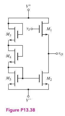
A simple output stage for an NMOS op-amp is shown in Figure P13.38. Device \(M_{1}\) operates as a source follower. The bias voltages are \(V^{+}=3 \mathrm{~V}\) and \(V^{-}=-3 \mathrm{~V}\). Transistor parameters are \(k_{n}^{\prime}=100 \mu \mathrm{A} / \mathrm{V}^{2}, V_{T N}=\) \(0.4
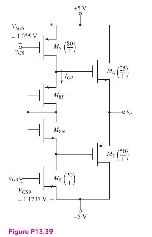
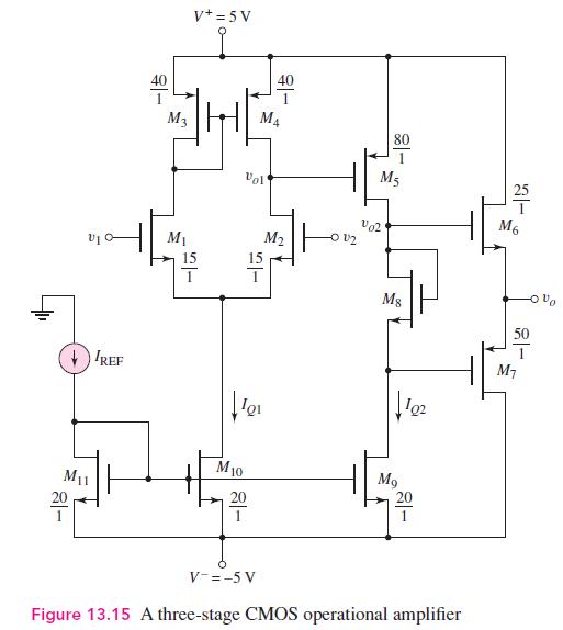
The circuit in Figure P13.39 is another form of an output stage for the CMOS op-amp shown in Figure 13.15. Assume the same transistor parameters as given in Example 13.10. The width-to-length values of some transistors are given and the applied gate-to-source voltages of \(M_{5}\) and \(M_{9}\) are
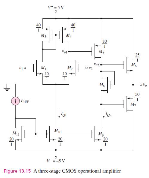
Consider the three-stage CMOS op-amp in Figure 13.15. Design an allNMOS transistor current source circuit to establish \(I_{Q 1}=150 \mu \mathrm{A}\). The NMOS transistor parameters are \(k_{n}^{\prime}=100 \mu \mathrm{A} / \mathrm{V}^{2}\) and \(V_{T N}=0.5 \mathrm{~V}\). Assume the minimum
Assume \(I_{\mathrm{REF}}=250 \mu \mathrm{A}\) and \((W / L)_{8}=5\) in the CMOS op-amp shown in Figure 13.15. Determine (a) the quiescent currents in \(M_{6}\) and \(M_{7}\) and (b) the overall small-signal voltage gain. Assume transistor parameters as given in Example 13.10.Data From Example
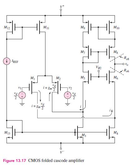
The CMOS folded cascode circuit in Figure 13.17 is biased at \(\pm 5 \mathrm{~V}\) and the reference current is \(I_{\mathrm{REF}}=50 \mu \mathrm{A}\). The transistor parameters are \(V_{T N}=0.5 \mathrm{~V}, V_{T P}=-0.5 \mathrm{~V}, K_{n}=K_{p}=0.5 \mathrm{~mA} / \mathrm{V}^{2}\), and
The CMOS folded cascode amplifier in Figure 13.17 is to be redesigned to provide a differential voltage gain of 10,000 . The biasing is the same as described in Problem 13.42. The transistor parameters are \(V_{T N}=0.5 \mathrm{~V}\), \(V_{T P}=-0.5 \mathrm{~V}, k_{n}^{\prime}=80 \mu \mathrm{A} /
The CMOS folded cascode amplifier of Figure 13.17 is to be designed to provide a differential voltage gain of 25,000 . The maximum power dissipated in the circuit is to be limited to \(3 \mathrm{~mW}\). Assume transistor parameters as described in Problem 13.43, except the relation between NMOS and
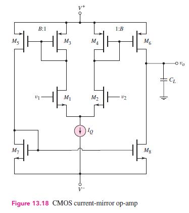
The bias current in the CMOS current-gain op-amp in Figure 13.18 is \(I_{Q}=120 \mu \mathrm{A}\). The transistor parameters are \(V_{T N}=0.5 \mathrm{~V}, V_{T P}=-0.5 \mathrm{~V}\), \(k_{n}^{\prime}=100 \mu \mathrm{A} / \mathrm{V}^{2}, k_{p}^{\prime}=40 \mu \mathrm{A} / \mathrm{V}^{2},
The CMOS current gain op-amp in Figure 13.18 is to be redesigned to provide a differential voltage gain of 400 . The transistor parameters are \(V_{T N}=0.5 \mathrm{~V}, V_{T P}=-0.5 \mathrm{~V}, k_{n}^{\prime}=80 \mu \mathrm{A} / \mathrm{V}^{2}, k_{p}^{\prime}=35 \mu \mathrm{A} / \mathrm{V}^{2},
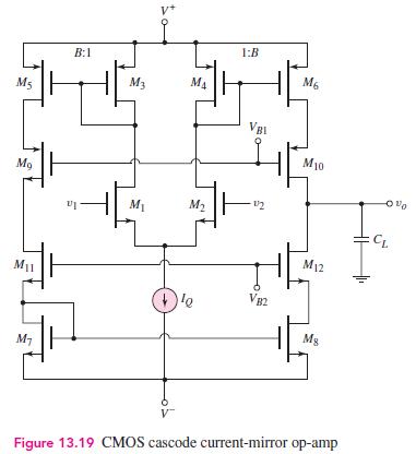
Redesign the CMOS cascode current mirror in Figure 13.19 to provide a differential voltage gain of 20,000. The bias current and transistor parameters are the same as in Problem 13.46. (a) Design the basic amplifier to provide the specified voltage gain. (b) Design a current source to provide the
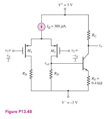
A simple BiCMOS amplifier is shown in Figure P13.48. The MOS transistor parameters are \(k_{p}^{\prime}=40 \mu \mathrm{A} / \mathrm{V}^{2}, V_{T P}=-0.4 \mathrm{~V}, \lambda=0\), and \((W / L)_{1,2}=50\), and the bipolar transistor parameters are \(V_{B E}(\) on \()=0.7 \mathrm{~V}, \beta=120\),
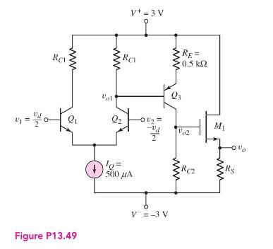
Consider the simple BiCMOS amplifier shown in Figure P13.49. The bipolar transistor parameters are \(\beta_{n}=\beta_{p}=120, V_{B E}\) (on) \(=V_{E B}(\) on \()=0.7 \mathrm{~V}\), \(V_{A}=\infty\), and the MOS transistor parameters are \(V_{T N}=0.4 \mathrm{~V}, K_{n}=\) \(3 \mathrm{~mA} /
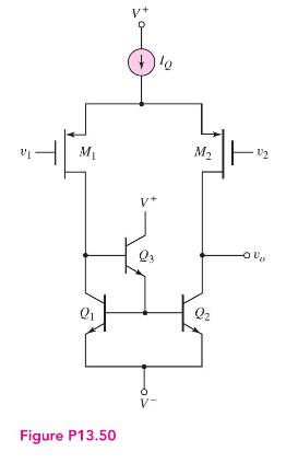
A BiCMOS amplifier is shown in Figure P13.50. The transistor parameters \(\operatorname{are} V_{T P}=-0.4 \mathrm{~V}, k_{p}^{\prime}=40 \mu \mathrm{A} / \mathrm{V}^{2}, W / L=40, \lambda=0.035 \mathrm{~V}^{-1}, \beta=120\), and \(V_{A}=150 \mathrm{~V}\). The bias current is \(I_{Q}=250 \mu
Design a BiCMOS amplifier that is complementary to the one in Figure P13.50 in that the input devices are NMOS and the load transistors are pnp. Assume transistor parameters of \(V_{T N}=0.4 \mathrm{~V}, k_{n}^{\prime}=100 \mu \mathrm{A} / \mathrm{V}^{2}\), \(W / L=40, \lambda=0.02
The reference current in the BiCMOS folded cascode amplifier in Figure 13.20 is \(I_{\mathrm{REF}}=200 \mu \mathrm{A}\) and the circuit bias voltages are \(\pm 10 \mathrm{~V}\). The MOS transistor parameters are the same as in Problem 13.42. The BJT parameters are \(\beta=120\) and \(V_{A}=80
The BiCMOS folded cascode amplifier in Figure 13.20 is to be designed to provide a differential voltage gain of 25,000 . The maximum power dissipated in the circuit is to be limited to \(10 \mathrm{~mW}\). Assume MOS transistor parameters as described in Problem 13.43. The BJT parameters are
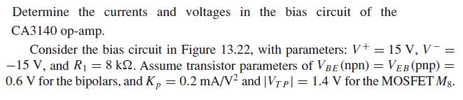
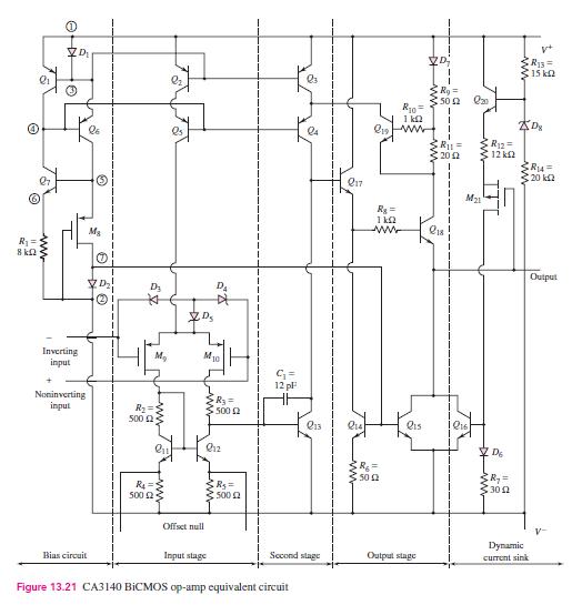
If the CA3140 op-amp is biased at \(V^{+}=15 \mathrm{~V}\) and \(V^{-}=-15 \mathrm{~V}\), determine the input common-mode voltage range. Assume B-E voltages of \(0.6 \mathrm{~V}\) for the bipolar transistors and \(\left|V_{T P}\right|=1.4 \mathrm{~V}\) for the MOSFETs.
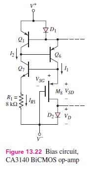
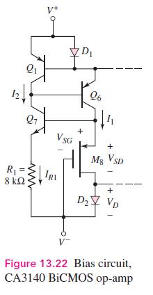
Consider the bias circuit portion of the CA3140 op-amp in Figure 13.22. If \(V_{B E 7}=0.6 \mathrm{~V}\) for \(Q_{7}\) and \(V_{T P}=-1.0 \mathrm{~V}\) for \(M_{8}\), determine the required value of the conduction parameter for \(M_{8}\) such that \(I_{1}=I_{2}=150 \mu \mathrm{A}\). V+ Di 26 21 R =
In the bias portion of the CA1340 op-amp in Figure 13.22, the bipolar transistor parameters are \(V_{B E}(\mathrm{npn})=0.6 \mathrm{~V}\) and \(V_{E B}(\mathrm{pnp})=0.6 \mathrm{~V}\) and the MOSFET parameters are \(V_{T P}=-1.2 \mathrm{~V}\) and \(K_{p}=0.15 \mathrm{~mA} / \mathrm{V}^{2}\). (a)
Consider the CA3140 op-amp in Figure 13.21. If the bias currents change such that \(I_{C 5}=I_{C 4}=300 \mu \mathrm{A}\), determine the voltage gains of the input and second stages, and find the overall voltage gain. D R = 8 Mg e D3 57 DS Da Inverting input M M10 Noninverting input Ry 500 2 Bias
Assume the gain stage of the CA3140 op-amp is modified to include an emitter resistor, as shown in Figure 13.23. Let \(\lambda=0.02 \mathrm{~V}^{-1}\) for \(M_{10}\). If the transistor bias currents in \(M_{10}\) and \(Q_{12}\) are \(150 \mu \mathrm{A}\) and the current in \(Q_{13}\) is \(300 \mu
In the LF155 BiFET op-amp in Figure 13.25, the combination of \(Q_{3}, J_{6}\), and \(Q_{4}\) establishes the reference bias current. Assume the power supply voltages are \(V^{+}=10 \mathrm{~V}\) and \(V^{-}=-10 \mathrm{~V}\). The transistor parameters are \(V_{E B}(\mathrm{on})=\) \(0.6
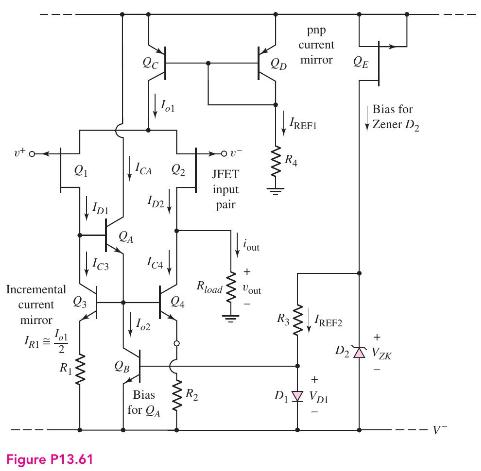
Consider the circuit in Figure P13.60. A JFET diff-amp input stage drives a bipolar Darlington second stage. The p-channel differential pair \(J_{1}\) and \(J_{2}\) are connected to the bipolar active load transistors \(Q_{3}\) and \(Q_{4}\). Assume JFET parameters of \(V_{P}=3 \mathrm{~V}, I_{D S
Consider the BiFET differential input stage in Figure P13.61, biased with power supply voltages \(V^{+}\)and \(V^{-}\). Let \(V^{+}=-V^{-} \equiv V_{S}\). (a) Design the bias circuit such that \(I_{\mathrm{REF} 2}=100 \mu \mathrm{A}\) for supply voltages in the range \(3 \leq V_{S} \leq 12
The BiFET diff-amp input stage in Figure P13.61 is biased at \(I_{O 1}=1 \mathrm{~mA}\). The JFET parameters are \(V_{P}=4 \mathrm{~V}, I_{D S S}=1 \mathrm{~mA}\), and \(\lambda=0.02 \mathrm{~V}^{-1}\). The bipolar transistor parameters are \(\beta=200\) and \(V_{A}=100\) V. (a) For
Consider the input stage and bias circuit of the 741 op-amp in Figure 13.5. Transistor \(Q_{10}\) may be replaced by a constant-current source equal to \(19 \mu \mathrm{A}\). Assume: the npn devices have parameters \(\beta=200\) and \(V_{A}=150\) \(\mathrm{V}\); the pnp devices have parameters
The output stage of the 741 op-amp is shown in Figure 13.9. Transistor \(Q_{13}\) may be replaced with a constant-current source equal to \(0.18 \mathrm{~mA}\). Use standard transistors. (a) Using a computer simulation, plot the voltage transfer function \(v_{o}\) versus \(v_{13}\). What is the
Consider the BiCMOS input stage of the CA3140 op-amp in Figure 13.21. Transistor \(Q_{5}\) can be replaced with a constant-current source of \(200 \mu \mathrm{A}\). Assume: bipolar transistor parameters of \(\beta=200, I_{E O}=10^{-14} \mathrm{~A}\), and \(V_{A}=50 \mathrm{~V}\); and MOSFET
Consider the CMOS op-amp in Figure 13.14. Assume the circuit and transistor parameters are as given in Example 13.8. In addition, let \(\lambda=\) \(0.01 \mathrm{~V}^{-1}\) for all transistors. (a) Determine the overall low-frequency differential voltage gain. Compare these results with those in
Consider the input stage and bias circuit of the 741 op-amp shown in Figure 13.5. Design a complementary circuit such that the input transistors are pnp devices, and the bias currents are \(I_{\text {REF }}=0.4 \mathrm{~mA}\) and \(I_{C 10}=24 \mu \mathrm{A}\) when the circuit is biased at \(\pm 5
Redesign the CMOS op-amp in Figure 13.14 to provide a minimum overall voltage gain of at least 50,000 . The bias voltages are \(V^{+}=10 \mathrm{~V}\) and \(V^{-}=-10 \mathrm{~V}\). The threshold voltage is \(\left|V_{T}\right|=1 \mathrm{~V}\) for all transistors, and \(\lambda=0.01
Showing 300 - 400
of 4723
1
2
3
4
5
6
7
8
9
10
11
12
13
14
15
Last
Step by Step Answers