New Semester
Started
Get
50% OFF
Study Help!
--h --m --s
Claim Now
Question Answers
Textbooks
Find textbooks, questions and answers
Oops, something went wrong!
Change your search query and then try again
S
Books
FREE
Study Help
Expert Questions
Accounting
General Management
Mathematics
Finance
Organizational Behaviour
Law
Physics
Operating System
Management Leadership
Sociology
Programming
Marketing
Database
Computer Network
Economics
Textbooks Solutions
Accounting
Managerial Accounting
Management Leadership
Cost Accounting
Statistics
Business Law
Corporate Finance
Finance
Economics
Auditing
Tutors
Online Tutors
Find a Tutor
Hire a Tutor
Become a Tutor
AI Tutor
AI Study Planner
NEW
Sell Books
Search
Search
Sign In
Register
study help
computer science
systems analysis and design 12th
Microelectronics Circuit Analysis And Design 4th Edition Donald A. Neamen - Solutions
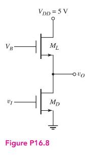
The enhancement-load transistor in the NMOS inverter in Figure P16.8 has a separate bias applied to the gate. Assume transistor parameters of \(K_{n}=1 \mathrm{~mA} / \mathrm{V}^{2}\) for \(M_{D}, K_{n}=0.4 \mathrm{~mA} / \mathrm{V}^{2}\) for \(M_{L}\), and \(V_{T N}=1 \mathrm{~V}\) for both
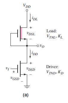
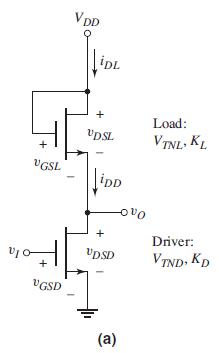
For the depletion load inverter shown in Figure 16.7(a), assume parameters of \(V_{D D}=3.3 \mathrm{~V}, V_{T N D}=0.5 \mathrm{~V}, V_{T N L}=-0.8 \mathrm{~V}, K_{D}=500 \mu \mathrm{A} / \mathrm{V}^{2}\), and \(K_{L}=100 \mu \mathrm{A} / \mathrm{V}^{2}\). (a) Find the transition points of the
In the depletion-load NMOS inverter circuit in Figure 16.7(a), let \(V_{T N D}=0.5 \mathrm{~V}\) and \(V_{D D}=3 \mathrm{~V}, K_{L}=50 \mu \mathrm{A} / \mathrm{V}^{2}\), and \(K_{D}=500 \mu \mathrm{A} / \mathrm{V}^{2}\). Calculate the value of \(V_{T N L}\) such that \(v_{O}=0.10 \mathrm{~V}\) when
Consider the NMOS inverter with depletion load in Figure 16.7(a). Let \(V_{D D}=1.8 \mathrm{~V}\), and assume \(V_{T N D}=0.3 \mathrm{~V}\) and \(V_{T N L}=-0.6 \mathrm{~V}\).(a) Design the circuit such that the power dissipation is \(80 \mu \mathrm{W}\) and the output voltage is \(v_{O}=0.06
The NMOS inverter with depletion load is shown in Figure 16.7(a). The bias is \(V_{D D}=2.5 \mathrm{~V}\). The transistor parameters are \(V_{T N D}=0.5 \mathrm{~V}\) and \(V_{T N L}=-1 \mathrm{~V}\). The width-to-length ratio of the load device is \(W / L=1\). (a) Design the driver transistor such
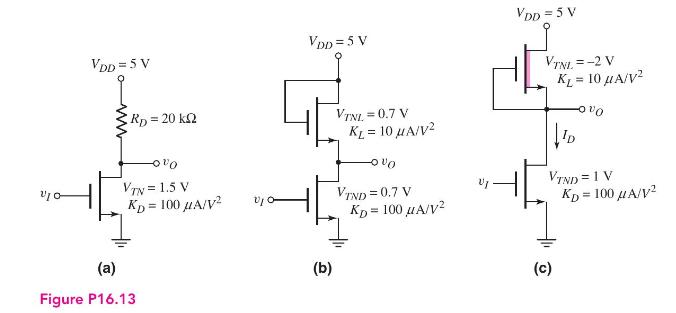
Calculate the power dissipated in each inverter circuit in Figure P16.13 for the following input conditions: (a) Inverter a: (i) \(v_{I}=0.5 \mathrm{~V}\), (ii) \(v_{I}=5 \mathrm{~V}\); (b) Inverter b: (i) \(v_{I}=0.25 \mathrm{~V}\), (ii) \(v_{I}=4.3 \mathrm{~V}\); (c) Inverter \(\mathrm{c}\) : (i)
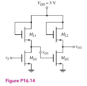
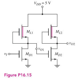
For the two inverters in Figure P16.14, assume \((W / L)_{L}=1\) for the load devices and \((W / L)_{D}=10\) for the driver devices.(a) If \(v_{I}\) is a logic 1 , determine the values of \(v_{O 1}\) and \(v_{O 2}\).(b) Repeat part (a) if \(v_{I}\) is a logic 0 . 1 VDD=5 V MLI ML2 01/02 MD1 Figure
Consider the circuit in Figure P16.15. The parameters of the driver transistors are \(V_{T N D}=0.8 \mathrm{~V}\) and \((W / L)_{D}=4\), and those of the load transistors are \(V_{T N L}=-1.2 \mathrm{~V}\) and \((W / L)_{L}=1\).(a) If \(v_{I}\) is a logic 1 , determine the values of \(v_{O 1}\) and
For the saturated load inverter shown in Figure 16.9(a), assume transistor parameters of \(V_{T N D O}=V_{T N L O}=0.5 \mathrm{~V}, \quad K_{D}=200 \mu \mathrm{A} / \mathrm{V}^{2}, \quad K_{L}=\) \(20 \mu \mathrm{A} / \mathrm{V}^{2}, \quad \gamma=0.25 \mathrm{~V}^{1 / 2}, \quad\) and \(\phi_{f
Consider the NMOS inverter with depletion load in Figure 16.9(b). The transistor parameters are \(V_{T N D O}=0.4 \mathrm{~V}, \quad V_{T N L O}=-0.6 \mathrm{~V}, K_{D}=\) \(100 \mu \mathrm{A} / \mathrm{V}^{2}, K_{L}=20 \mu \mathrm{A} / \mathrm{V}^{2}, \gamma=0.25 \mathrm{~V}^{1 / 2}\), and
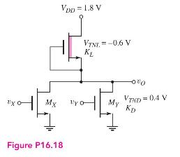
Consider the circuit with a depletion load device shown in Figure P16.18.(a) For \(v_{X}=1.8 \mathrm{~V}\) and \(v_{Y}=0.1 \mathrm{~V}\), determine \(K_{D} / K_{L}\) such that \(v_{O}=0.1 \mathrm{~V}\).(b) Using the results of part (a), determine \(v_{O}\) when \(v_{X}=v_{Y}=1.8 \mathrm{~V}\).(c)
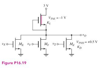
Consider the three-input NOR logic gate in Figure P16.19. The transistor parameters are \(V_{T N L}=-1 \mathrm{~V}\) and \(V_{T N D}=0.5 \mathrm{~V}\). The maximum value of \(v_{O}\) in its low state is to be \(0.1 \mathrm{~V}\). (a) Determine \(K_{D} / K_{L}\). (b) The maximum power dissipation in
Consider a four-input NMOS NOR logic gate with a depletion load similar to the circuit in Figure P16.19. Assume \(V_{D D}=2.5 \mathrm{~V}, V_{T N D}=0.4 \mathrm{~V}\), and \(V_{T N L}=-0.6 \mathrm{~V}\). The maximum value of \(v_{O}\) in its low state is to be \(50 \mathrm{mV}\). (a) Determine
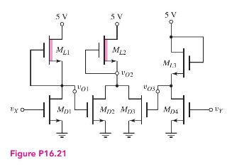
The transistor parameters for the circuit in Figure P16.21 are: \(V_{T N}=0.8 \mathrm{~V}\) for all enhancement-mode devices, \(V_{T N}=-2 \mathrm{~V}\) for the depletion-mode devices, and \(k_{n}^{\prime}=60 \mu \mathrm{A} / \mathrm{V}^{2}\) for all devices. The width-to-length ratios of \(M_{L
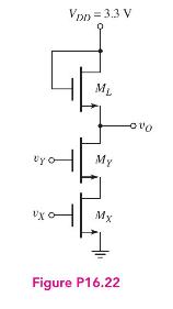
Consider the NMOS circuit in Figure P16.22. The transistor parameters are \((W / L)_{X}=(W / L)_{Y}=12,(W / L)_{L}=1\), and \(V_{T N}=0.4 \mathrm{~V}\). Neglect the body effect. (a) Determine \(v_{O}\) when \(v_{X}=v_{Y}=2.9 \mathrm{~V}\). (b) What are the values of \(v_{G S X}, v_{G S Y}, v_{D S
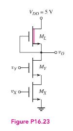
In the NMOS circuit in Figure P16.23, the transistor parameters are: \((W / L)_{X}=(W / L)_{Y}=4,(W / L)_{L}=1, V_{T N X}=V_{T N Y}=0.8 \mathrm{~V}\), and \(V_{T N L}=\) \(-1.5 \mathrm{~V}\).(a) Determine \(v_{O}\) when \(v_{X}=v_{Y}=5 \mathrm{~V}\).(b) What are the values of \(v_{G S X}, v_{G S
Consider a four-input NMOS NAND logic gate with a depletion load similar to the circuit in Figure P16.23. The bias voltage is \(V_{D D}=3.3 \mathrm{~V}\), and the threshold voltages are \(V_{T N D}=0.4 \mathrm{~V}\) and \(V_{T N L}=-0.6 \mathrm{~V}\). The logic 0 output voltage is to be \(0.10
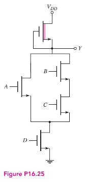
Determine the logic function implemented by the circuit in Figure P16.25. Vn DD T Figure P16.25
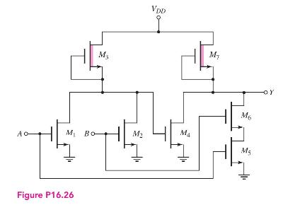
Find the logic function implemented by the circuit in Figure P16.26. My A M Bo M Figure P16.26 VDD M M6 MA Ms
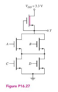
What is the logic function implemented by the circuit in Figure P16.27. Vop=3.3V T T D Figure P16.27
The Boolean function for a carry-out signal of a one-bit full adder is given by\[\text { Carry-out }=A \cdot B+A \cdot C+B \cdot C\](a) Design an NMOS logic circuit with depletion load to perform this function. Signals \(A, B\), and \(C\) are available. (b) Assume \((W / L)_{L}=1\), \(V_{D D}=5
(a) Design an NMOS depletion-load logic gate that implements the function \(\bar{Y}=[A+B \cdot(C+D)]\). (b) Assume \(V_{D D}=2.5 \mathrm{~V},(W / L)_{L}=1\), \(V_{T N D}=0.4 \mathrm{~V}\), and \(V_{T N L}=-0.6 \mathrm{~V}\). Determine \((W / L)_{D}\) of each transistor such that \(V_{O L}(\max )=50
Design an NMOS logic circuit with a depletion load that will sound an alarm in an automobile if the ignition is turned off while the headlights are still on and/or the parking brake has not been set. Separate indicator lights are also to be included showing whether the headlights are on or the
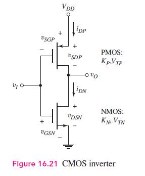
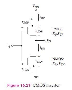
Consider the CMOS inverter in Figure 16.21 biased at \(V_{D D}=2.5 \mathrm{~V}\). The transistor parameters are \(V_{T N}=0.4 \mathrm{~V}, V_{T P}=-0.4 \mathrm{~V}\), and \(K_{n}=\) \(K_{p}=100 \mu \mathrm{A} / \mathrm{V}^{2}\). (a) Find the transition points for the p-channel and \(\mathrm{n}\)
For the CMOS inverter in Figure 16.21, let \(V_{D D}=3.3 \mathrm{~V}, k_{n}^{\prime}=100 \mu \mathrm{A} / \mathrm{V}^{2}\), \(k_{p}^{\prime}=40 \mu \mathrm{A} / \mathrm{V}^{2}, V_{T N}=0.4 \mathrm{~V}\), and \(V_{T P}=-0.4 \mathrm{~V}\).(a) Let \((W / L)_{n}=2\) and \((W / L)_{p}=5\). (i) Find the
(a) For the CMOS inverter in Figure 16.21 in the text, let \(V_{D D}=3.3 \mathrm{~V}\), \(V_{T N}=+0.4 \mathrm{~V}\), and \(V_{T P}=-0.4 \mathrm{~V}\). Assume \((W / L)_{n}=4\) and \((W / L)_{p}=12\). Determine (i) the input switching voltage, (ii) the input voltage when \(v_{O}=3.1 \mathrm{~V}\),
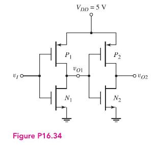
Consider the CMOS inverter pair in Figure P16.34. Let \(V_{T N}=0.8 \mathrm{~V}\), \(V_{T P}=-0.8 \mathrm{~V}\), and \(K_{n}=K_{p}\). (a) If \(v_{O 1}=0.6 \mathrm{~V}\), determine \(v_{I}\) and \(v_{O 2}\). (b) Determine the range of \(v_{02}\) for which both \(N_{2}\) and \(P_{2}\) are biased in
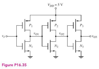
Consider the series of CMOS inverters in Figure P16.35. The threshold voltages of the n-channel transistors are \(V_{T N}=0.8 \mathrm{~V}\), and the threshold voltages of the p-channel transistors are \(V_{T P}=-0.8 \mathrm{~V}\). The conduction parameters are all equal. (a) Determine the range of
(a) A CMOS inverter is biased at \(V_{D D}=2.5 \mathrm{~V}\). The transistor parameters are \(K_{n}=K_{p}=120 \mu \mathrm{A} / \mathrm{V}^{2}, V_{T N}=0.4 \mathrm{~V}\), and \(V_{T P}=-0.4 \mathrm{~V}\). Calculate and plot the current in the transistors as a function of the input voltage for \(0
The transistor parameters in the CMOS inverter are \(V_{T N}=0.35 \mathrm{~V}\), \(V_{T P}=-0.35 \mathrm{~V}, k_{n}^{\prime}=80 \mu \mathrm{A} / \mathrm{V}^{2}\), and \(k_{p}^{\prime}=40 \mu \mathrm{A} / \mathrm{V}^{2}\). Let \(V_{D D}=1.8 \mathrm{~V}\).(a) Determine the peak current in the
A CMOS inverter is biased at \(V_{D D}=3.3 \mathrm{~V}\). The transistor threshold voltages are \(V_{T N}=+0.4 \mathrm{~V}\) and \(V_{T P}=-0.4 \mathrm{~V}\). Determine the peak current in the inverter and the input voltage at which it occurs for (a) \((W / L)_{n}=3,(W / L)_{p}=\) 7.5; (b) \((W /
A load capacitor of \(0.2 \mathrm{pF}\) is connected to the output of a CMOS inverter. Determine the power dissipated in the CMOS inverter for a switching frequency of \(10 \mathrm{MHz}\), for inverter parameters described in (a) Problem 16.36 and (b) Problem 16.37.Data From Problem 16.36:-(a) A
(a) A CMOS digital logic circuit contains the equivalent of 4 million CMOS inverters and is biased at \(V_{D D}=1.8 \mathrm{~V}\). The equivalent load capacitance of each inverter is \(0.12 \mathrm{pF}\) and each inverter is switching at \(150 \mathrm{MHz}\). Determine the total average power
A particular IC chip can dissipate \(3 \mathrm{~W}\) and contains 10 million CMOS inverters. Each inverter is being switched at a frequency \(f\). (a) Determine the average power that each inverter can dissipate without exceeding the total allowed power. (b) If the switching frequency is \(f=5
Repeat Problem 16.41 for the case when the chip contains 5 million CMOS inverters being switched at \(f=8 \mathrm{MHz}\) and the total power dissipated can be \(10 \mathrm{~W}\).Data From Problem 16.41:-A particular IC chip can dissipate \(3 \mathrm{~W}\) and contains 10 million CMOS inverters.
Consider a CMOS inverter. (a) Show that when \(v_{I} \cong V_{D D}\), the resistance of the NMOS device is approximately \(1 /\left[k_{n}^{\prime}(W / L)_{n}\left(V_{D D}-V_{T N}\right)\right]\), and when \(v_{I} \cong 0\), the resistance of the PMOS device is approximately \(1
The CMOS inverter in Figure 16.21 is biased at \(V_{D D}=3.3 \mathrm{~V}\). Let \(K_{n}=K_{p}\), \(V_{T N}=0.5 \mathrm{~V}\), and \(V_{T P}=-0.5 \mathrm{~V}\). (a) Determine the two values of \(v_{I}\) and the corresponding values of \(v_{O}\) for which \(\left(d v_{O} / d v_{I}\right)=-1\) on the
Repeat Problem 16.44 if the circuit and transistor parameters are \(V_{D D}=2.5 \mathrm{~V}\), \(V_{T N}=0.35 \mathrm{~V}, V_{T P}=-0.35 \mathrm{~V}, K_{n}=100 \mu \mathrm{A} / \mathrm{V}^{2}\), and \(K_{p}=50 \mu \mathrm{A} / \mathrm{V}^{2}\).Data From Problem 16.44:-The CMOS inverter in Figure
(a) Determine the noise margins of a CMOS inverter biased at \(V_{D D}=3.3 \mathrm{~V}\) with \((W / L)_{n}=2\) and \((W / L)_{p}=5\). Assume \(V_{T N}=0.4 \mathrm{~V}\) and \(V_{T P}=\) \(-0.4 \mathrm{~V}\).(b) Repeat part (a) for \((W / L)_{n}=4\) and \((W / L)_{p}=12\).
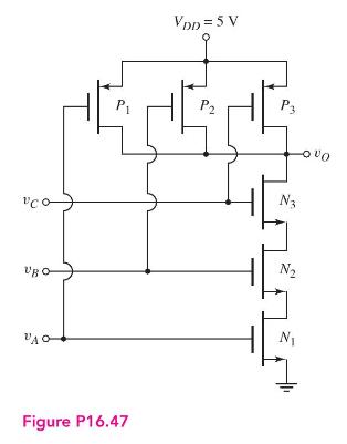
Consider the three-input CMOS NAND circuit in Figure P16.47. Assume \(k_{n}^{\prime}=2 k_{p}^{\prime}\) and \(V_{T N}=\left|V_{T P}\right|=0.8 \mathrm{~V}\).(a) If \(v_{A}=v_{B}=5 \mathrm{~V}\), determine \(v_{C}\) such that both \(N_{3}\) and \(P_{3}\) are biased in the saturation region when \((W
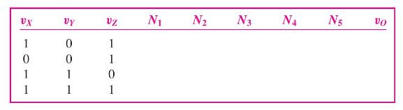
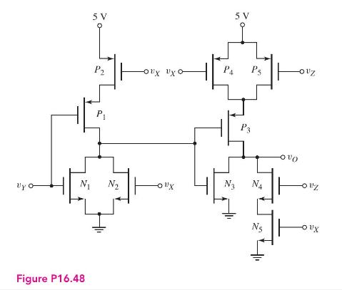
Consider the circuit in Figure P16.48. (a) The inputs \(v_{X}, v_{Y}\), and \(v_{Z}\) listed in the following table are either a logic 0 or a logic 1 . These inputs are the outputs from similar-type CMOS logic circuits. The input logic conditions listed are sequential in time. State whether the
Consider a four-input CMOS NOR logic gate. Determine the \(W / L\) ratios of the transistors to provide for symmetrical switching based on the CMOS inverter design with \((W / L)_{n}=2\) and \((W / L)_{p}=4\). (b) If the load capacitance of the NOR gate doubles, determine the required \(W / L\)
Repeat Problem 16.49 for a four-input CMOS NAND logic gate.Data From Problem 16.49:-Consider a four-input CMOS NOR logic gate. Determine the \(W / L\) ratios of the transistors to provide for symmetrical switching based on the CMOS inverter design with \((W / L)_{n}=2\) and \((W / L)_{p}=4\). (b)
Repeat Problem 16.49 for a three-input CMOS NOR logic gate.Data From Problem 16.49:-Consider a four-input CMOS NOR logic gate. Determine the \(W / L\) ratios of the transistors to provide for symmetrical switching based on the CMOS inverter design with \((W / L)_{n}=2\) and \((W / L)_{p}=4\). (b)
Repeat Problem 16.49 for a three-input CMOS NAND logic gate.Data From Problem 16.49:-Consider a four-input CMOS NOR logic gate. Determine the \(W / L\) ratios of the transistors to provide for symmetrical switching based on the CMOS inverter design with \((W / L)_{n}=2\) and \((W / L)_{p}=4\). (b)
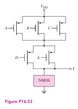
Figure P16.53 shows a classic CMOS logic circuit. (a) What is the logic function performed by the circuit? (b) Design the NMOS network. (c) Determine the transistor \(W / L\) ratios to provide symmetrical switching times at twice the switching speed of the basic CMOS inverter with \((W / L)_{n}=2\)
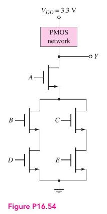
Figure P16.54 is a classic CMOS logic gate. (a) What is the logic function performed by the circuit? (b) Design the PMOS network. (c) Determine the transistor \(W / L\) ratios to provide symmetrical switching times at twice the switching speed as the basic CMOS inverter with \((W / L)_{n}=2\) and
Figure P16.55 is a classic CMOS logic gate. (a) What is the logic function performed by the circuit? (b) Design the NMOS network. (c) Determine the transistor \(W / L\) ratios to provide symmetrical switching times equal to the basic CMOS inverter with \((W / L)_{n}=2\) and \((W / L)_{p}=4\). B VDD
Consider the classic CMOS logic circuit in Figure P16.56. (a) What is the logic function performed by the circuit? (b) Design the PMOS network. (c) Determine the transistor \(W / L\) ratios to provide symmetrical switching times equal to the basic CMOS inverter with \((W / L)_{n}=2\) and \((W /
(a) Given inputs \(A, B, C, \bar{A}, \bar{B}\), and \(\bar{C}\), design a CMOS circuit to implement the logic function \(Y=A \bar{B} \bar{C}+\bar{A} \bar{B} C+\bar{A} B \bar{C}\). The design should not include a CMOS inverter at the output. (b) For \(k_{n}^{\prime}=2 k_{p}^{\prime}\), size the
(a) Given inputs \(A, B, C, D\), and \(E\), design a CMOS circuit to implement the logic function \(\bar{Y}=A(B+C)+D+E\).(b) Repeat part (b) of Problem 16.57 for this circuit.Data From Problem 16.57:-(a) Given inputs \(A, B, C, \bar{A}, \bar{B}\), and \(\bar{C}\), design a CMOS circuit to implement
(a) Determine the logic function performed by the circuit in Figure P16.59. (b) Determine the \(W / L\) ratios to provide symmetrical switching times equal to the basic CMOS inverter with \((W / L)_{n}=2\) and \((W / L)_{p}=4\). A 10- PMOS D VDD C A o Bo C A D Figure 16.59 CMOS pass logic network
(a) Consider a five-input CMOS NOR logic gate. Design the \(W / L\) ratios of the transistors to provide symmetrical switching times equal to the basic CMOS inverter with \((W / L)_{n}=2\) and \((W / L)_{p}=4\).(b) Repeat part (a) for a five-input CMOS NAND logic gate.
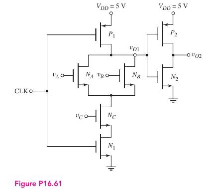
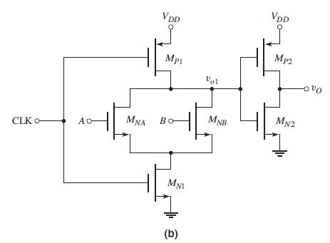
(a) Figure P16.61 shows a clocked CMOS logic circuit. Make a table showing the state of each transistor ("on" or "off"), and determine the output voltages \(v_{O 1}\) and \(v_{O 2}\) for the input logic states listed in the following table. Assume the input conditions are sequential in time from
(a) For the circuit in Figure P16.62, make a table showing the state of each transistor ("on" or "off"), and determine the output voltages \(v_{O 1}, v_{O 2}\), and \(v_{\mathrm{O} 3}\) for the input logic states listed in the following table. Assume the input conditions are sequential in time from
Sketch a clocked CMOS domino logic circuit that realizes the function \(Y=A \bar{B}+\bar{A} B\). Assume that both the variable and its complement are available as input signals.
Sketch a clocked CMOS domino logic circuit that realizes the function \(Y=A B+C(D+E)\).
Sketch a clocked CMOS domino logic circuit that realizes the function \(Y=A(B+C)(D+E)\)
Consider the CMOS clocked circuit in Figure 16.44(b). Assume the effective capacitance at the \(v_{O 1}\) terminal is \(25 \mathrm{fF}\). If the leakage current through the \(M_{N A}\) and \(M_{N B}\) transistors is \(I_{\text {Leakage }}=2 \mathrm{pA}\) when these transistors and \(M_{P 1}\) are
The parameters of an NMOS transmission gate are \(V_{T N}=0.4 \mathrm{~V}\), \(K_{n}=0.15 \mathrm{~mA} / \mathrm{V}^{2}\), and \(C_{L}=0.2 \mathrm{pF}\).(a) For a gate voltage of \(\phi=3.3 \mathrm{~V}\), determine the quasi-steady-state output voltage for (i) \(v_{I}=0\), (ii) \(v_{I}=3.3
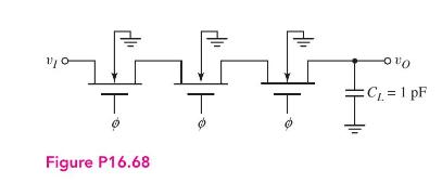
The NMOS transistors in the circuit shown in Figure P16.68 have parameters \(K_{n}=0.2 \mathrm{~mA} / \mathrm{V}^{2}, V_{T N}=0.5 \mathrm{~V}, \lambda=0\), and \(\gamma=0\).(a) For gate voltages of \(\phi=2.5 \mathrm{~V}\), determine the quasi-steady-state output voltage for (i) \(v_{I}=0\), (ii)
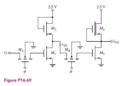
Consider the circuit shown in Figure P16.69. The input voltage \(v_{I}\) is either \(0.1 \mathrm{~V}\) or \(2.5 \mathrm{~V}\). Assume gate voltages of \(\phi=2.5 \mathrm{~V}\). The threshold voltages are \(V_{T N}=-0.6 \mathrm{~V}\) for \(M_{4}\) and \(V_{T N}=0.4 \mathrm{~V}\) for all other
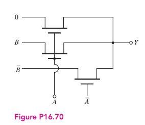
Consider the circuit in Figure P16.70. What logic function is implemented by this circuit? Are there any potential problems with this circuit? 0 B A Figure P16.70 T OY
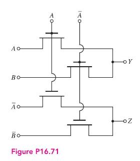
What is the logic function implemented by the circuit in Figure P16.71? A o Bo To Bo A Figure P16.71 A AO -OY -OZ
(a) Design an NMOS pass transistor logic circuit to perform the function \(Y=A+B(C+D)\). Assume that both the variable and its complement are available as input signals.(b) Repeat part (a) for the function \(Y=A B C+\bar{A} \bar{B} \bar{C}\).
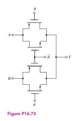
Consider the circuit in Figure P16.73.(a) Determine the value of \(Y\) for \(\phi=2.5 \mathrm{~V}\) and (i) \(A=B=0\); (ii) \(A=0, B=2.5 \mathrm{~V}\); (iii) \(A=2.5 \mathrm{~V}\), \(B=0\); and (iv) \(A=B=2.5 \mathrm{~V}\).(b) Repeat part (a) for \(\phi=0\).(c) What is the logic function
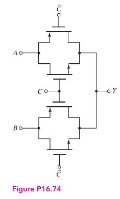
What is the logic function implemented by the circuit in Figure P16.74? Ao Figure P16.74 OY
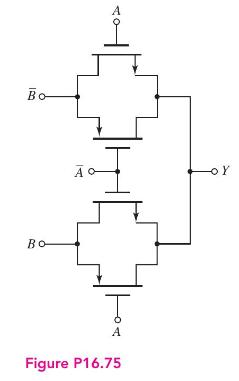
Consider the circuit in Figure P16.75. (a) Determine the value of \(Y\) for (i) \(A=B=0\); (ii) \(A=2.5 \mathrm{~V}, B=0\); (iii) \(A=0, B=2.5 \mathrm{~V}\); and (iv) \(A=B=2.5 \mathrm{~V}\). (b) What is the logic function implemented by the circuit? Bo Bo A Figure P16.75 OY
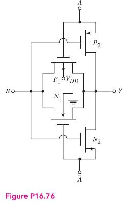
What is the logic function implemented by the circuit in Figure P16.76? Bo Figure P16.76 PVDD A P2 N OY
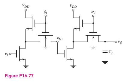
The circuit in Figure P16.77 is a form of clocked shift register. Signals \(\phi_{1}\) and \(\phi_{2}\) are nonoverlapping clock signals. Describe the operation of the circuit. Discuss any possible relationship between the width-to-length ratios of the load and driver transistors for "proper"
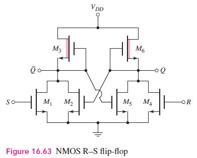
Consider the NMOS R-S flip-flop in Figure 16.63 biased at \(V_{D D}=2.5 \mathrm{~V}\). The threshold voltages are \(0.4 \mathrm{~V}\) (enhancement-mode devices) and \(-0.6 \mathrm{~V}\) (depletion-mode devices). The conduction parameters are \(K_{3}=\) \(K_{6}=40 \mu \mathrm{A} / \mathrm{V}^{2},
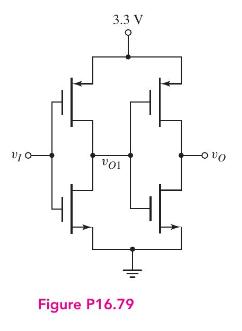
Figure P16.79 shows two CMOS inverters in cascade. This circuit can be thought of as an uncoupled CMOS R/S flip flop. The transistor parameters are \(K_{n}=K_{p}=0.2 \mathrm{~mA} / \mathrm{V}^{2}, V_{T N}=0.5 \mathrm{~V}, V_{T P}=-0.4 \mathrm{~V}\), and \(\lambda_{n}=\lambda_{p}=0\). Plot \(v_{O
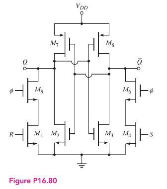
Consider the circuit in Figure P16.80. Determine the state of the outputs for various input signals. What is the purpose of the input signal \(\phi\) ? M VDD Mg M6 M5 b R M M M3 M4 -S Figure P16.80
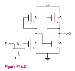
The circuit in Figure P16.81 is an example of a D flip-flop. (a) Explain the operation of the circuit. Is this a positive- or negative-edge-triggered flipflop? (b) Redesign the circuit to make this a static flip-flop. M2 VDD MA Do Ms M M3 CLK Figure P16.81
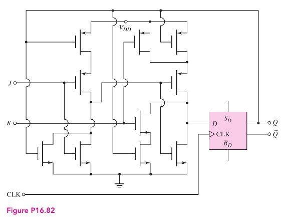
Show that the circuit in Figure P16.82 is a J-K flip-flop. CLK o Figure P16.82 VDD D Sp CLK RD
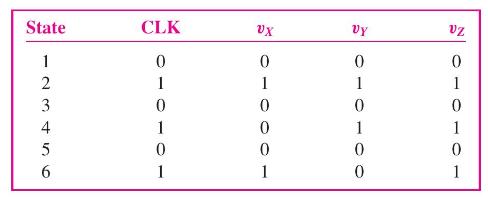
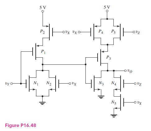
Reconsider the circuit shown in Figure P16.48. Show that this circuit is a \(\mathrm{J}-\mathrm{K}\) flip-flop with \(J=v_{X}, K=v_{Y}\), and CLK \(=v_{Z}\). 5 V 5V P2 P4 Ps P1 P3 vy O N N N3 N4 0z Figure P16.48
A 256-K memory is organized in a square array and uses the NMOS NOR decoder in Figure 16.73 (b) for the row- and column-decoders.(a) How many inputs does each decoder require?(b) What input to the row decoder is required to address row (i) 52 , (ii) 129 , and (iii) 241 ?(c) What input to the column
(a) A 1 megabit memory is organized in a square with each memory cell being individually addressed. Determine the number of input address lines required for the row and column decoders. (b) If the 1 megabit memory is organized as \(250 \mathrm{~K}\) words \(\times 4\) bits, determine the minimum
A 4096-bit RAM consists of 512 words of 8 bits each. Design the memory array to minimize the number of row and column address decoder transistors required. How many row and column address lines are required?
Assume that an NMOS address decoder can source \(250 \mu \mathrm{A}\) when the output goes high. If the effective capacitance of each memory cell is \(C_{L}=0.8 \mathrm{pF}\) and the effective capacitance of the address line is \(C_{L A}=5 \mathrm{pF}\), determine the rise time of the address line
Consider the NMOS RAM cell with resistor load in Figure 16.74(b). Assume parameters values of \(k_{n}^{\prime}=80 \mu \mathrm{A} / \mathrm{V}^{2}, V_{T N}=0.4 \mathrm{~V}, V_{D D}=2.5 \mathrm{~V}\), and \(R=1 \mathrm{M} \Omega\). (a) Design the width-to-length ratio of the driver transistor such
A 16-K NMOS RAM, with the cell design shown in Figure 16.74(b), is to dissipate no more than \(200 \mathrm{~mW}\) in standby when biased at \(V_{D D}=2.5 \mathrm{~V}\). Design the width-to-length ratios of the transistors and the resistance value. Assume \(V_{T N}=0.7 \mathrm{~V}\) and
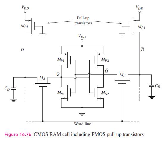
Consider the CMOS RAM cell and data lines in Figure 16.76 biased at \(V_{D D}=2.5 \mathrm{~V}\). Assume transistor parameters \(k_{n}^{\prime}=80 \mu \mathrm{A} / \mathrm{V}^{2}, k_{p}^{\prime}=35 \mu \mathrm{A} / \mathrm{V}^{2}\), \(V_{T N}=0.4 \mathrm{~V}, V_{T P}=-0.4 \mathrm{~V}, W /
Consider the CMOS RAM cell and data lines in Figure 16.76 with circuit and transistor parameters described in Problem 16.90. Assume initially that \(Q=0\) and \(\bar{Q}=1\). Assume the row is selected with \(X=2.5 \mathrm{~V}\) and assume the data lines, through a write cycle, are \(\bar{D}=0\) and
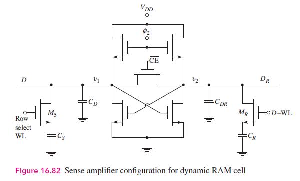
Consider a general sense amplifier configuration shown in Figure 16.82 for a dynamic RAM. Assume that each bit line has a capacitance of \(1 \mathrm{pF}\) and is precharged to \(4 \mathrm{~V}\). The storage capacitance is \(0.05 \mathrm{pF}\), the reference capacitance is \(0.025 \mathrm{pF}\), and
Design a 4-word \(\times\) 4-bit NMOS mask-programmed ROM to produce outputs of \(1011,1111,0110\), and 1001 when rows \(1,2,3\), and 4 , respectively, are addressed.
Design an NMOS \(16 \times 4\) mask-programmed ROM that provides the 4-bit product of two 2-bit variables.
Design an NMOS mask-programmed ROM that decodes a binary input and produces the output for a seven-segment array. The output is to be high when a particular LED is to be turned on.
An analog signal in the range 0 to \(5 \mathrm{~V}\) is to be converted to a digital signal with a quantization error of less than one percent. (a) What is the required number of bits? (b) What input voltage value represents 1 LSB? (c) What digital output represents an input voltage of \(3.5424
An analog signal in the range 0 to \(3.3 \mathrm{~V}\) is to be converted to a digital signal with a quantization error of less than 0.5 percent. (a) What is the required number of bits? (b) What input voltage value represents 1 LSB? (c) What digital output represents an input voltage of \(2.5321
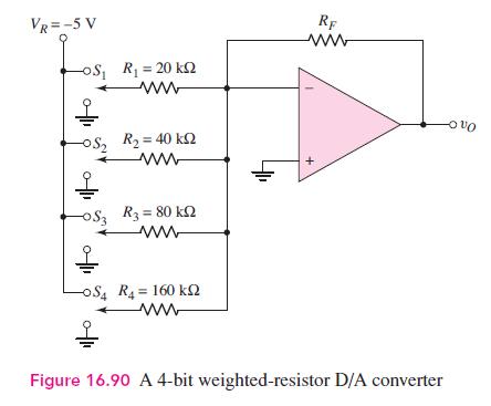
(a) What is the output voltage of the 4-bit weighted-resistor D/A in Figure 16.90 if the input is 0110 ? Assume \(R_{F}=10 \mathrm{k} \Omega\). (b) The input signal changes to 1001 . What is the output voltage? VR=-5 V OS R = 20 k ww OS R = 40 k ww -0S3 R3 = 80 k ww RF ww -OS4 R4 = 160 k ww Figure
Consider the 4-bit weighted-resistor D/A converter in Figure 16.90. Let \(R_{F}=10 \mathrm{k} \Omega\).(a) What is the maximum allowed tolerance ( \(\pm\) percent) in the value of \(R_{1}\) so that the maximum error in the output is limited to \(\pm \frac{1}{2}\) LSB?(b) Repeat part (a) for the
The weighted-resistor D/A converter in Figure 16.90 is to be expanded to an 8bit device. (a) What are the required resistance values of the additional four input resistors? (b) What is the output voltage if the input is 00000001 ? VR=-5 V OS R = 20 k ww OS R = 40 k ww -0S3 R3 = 80 k ww RF ww -OS4
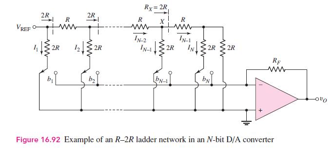
The \(N\)-bit \(\mathrm{D} / \mathrm{A}\) converter with an \(R-2 R\) ladder network in Figure 16.92 is to be designed as a 6-bit \(\mathrm{D} / \mathrm{A}\) device. Let \(V_{\mathrm{REF}}=-5.0 \mathrm{~V}\) and \(R=R_{F}=\) \(5.0 \mathrm{k} \Omega\). (a) What are currents \(I_{1}, I_{2}, I_{3},
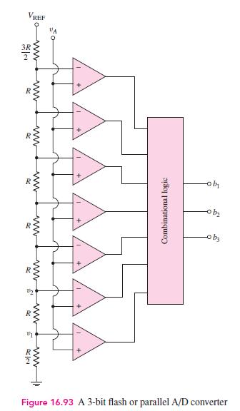
The 3-bit flash A/D converter in Figure 16.93 has a reference voltage of \(V_{\mathrm{REF}}=3.3 \mathrm{~V}\). The 3 -bit output is 101 . What is the range of \(v_{A}\) that produces this output? VREF ww 2 ww R R 190 -ob 0b3 Combinational logic ww ww ww wwww 5 R2 Figure 16.93 A 3-bit flash or
A 6-bit flash A/D converter, similar to the one in Figure 16.93, is to be fabricated. How many resistors and comparators are required? VREF ww 2 ww R R 190 -ob 0b3 Combinational logic ww ww ww wwww 5 R2 Figure 16.93 A 3-bit flash or parallel A/D converter
A 10-bit counting A/D converter has an analog input in the range \(0 \leq v_{A} \leq\) \(5 \mathrm{~V}\) and has a clock frequency of \(1 \mathrm{MHz}\). (a) What is the maximum conversion time? (b) If the output is 0010010010 , what is the range of the input signal \(v_{A}\) (assume a quantization
Consider the 10-bit counting A/D converter described in Problem 16.104.(a) What is the output if the analog input is \(v_{A}=3.125 \mathrm{~V}\) ?(b) Repeat part (a) if \(v_{A}=1.8613 \mathrm{~V}\).Data From Problem 16.104:-A 10-bit counting A/D converter has an analog input in the range \(0 \leq
Consider the three types of NMOS inverters shown in Figures 16.3(a), 16.5(a), and 16.7(a). Using a computer simulation, investigate the voltage transfer characteristics and the current versus input voltage characteristics of the three types of inverters as a function of various width-to-length
Using a computer simulation, investigate the propagation delay time and switching characteristics of a CMOS inverter by setting up a series of CMOS inverters in cascade. Use standard transistors and assume effective \(C_{T}\) load capacitances of \(0.05 \mathrm{pF}\). Determine the propagation
Showing 100 - 200
of 4723
1
2
3
4
5
6
7
8
9
10
11
12
13
14
15
Last
Step by Step Answers