New Semester
Started
Get
50% OFF
Study Help!
--h --m --s
Claim Now
Question Answers
Textbooks
Find textbooks, questions and answers
Oops, something went wrong!
Change your search query and then try again
S
Books
FREE
Study Help
Expert Questions
Accounting
General Management
Mathematics
Finance
Organizational Behaviour
Law
Physics
Operating System
Management Leadership
Sociology
Programming
Marketing
Database
Computer Network
Economics
Textbooks Solutions
Accounting
Managerial Accounting
Management Leadership
Cost Accounting
Statistics
Business Law
Corporate Finance
Finance
Economics
Auditing
Tutors
Online Tutors
Find a Tutor
Hire a Tutor
Become a Tutor
AI Tutor
AI Study Planner
NEW
Sell Books
Search
Search
Sign In
Register
study help
computer science
systems analysis and design 12th
Microelectronics Circuit Analysis And Design 4th Edition Donald A. Neamen - Solutions
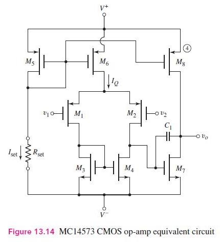
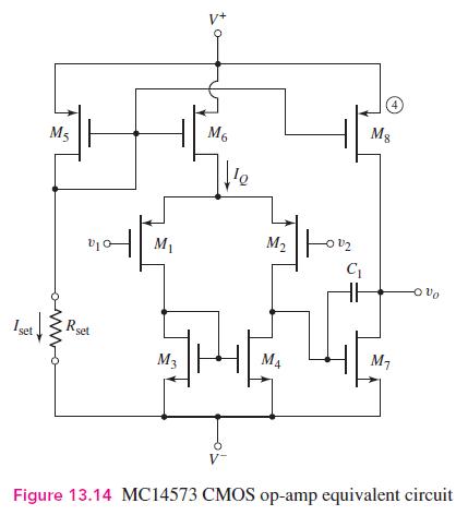
Consider the CMOS op-amp in Figure 13.14. Design a complementary CMOS circuit in which each element is replaced by its complement. The bias voltages are \(\pm 5 \mathrm{~V}\). The threshold voltage is \(\left|V_{T}\right|=0.7 \mathrm{~V}\) for all transistors, and \(\lambda=0.01 \mathrm{~V}^{-1}\)
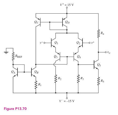
Consider the bipolar op-amp circuit in Figure P13.70. Design the circuit such that the differential gain is at least 800 , and the output voltage is zero when the input voltages are zero. The transistor current gains are 120 for all transistors, and the base-emitter voltages are \(0.6
List and describe five practical op-amp parameters and discuss the effect they have on op-amp circuit characteristics.
What is a typical value of open-loop, low-frequency gain of an op-amp circuit? How does this compare to the ideal value?
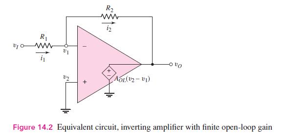
How does a finite open-loop gain affect the closed-loop gains of the inverting and noninverting amplifiers?
How does a finite open-loop gain affect the (a) input resistance of an op-amp circuit and (b) the output resistance of an op-amp circuit? Consider the inverting and noninverting amplifiers.
Describe the open-loop amplifier frequency response and define the unity-gain bandwidth.
What is a typical corner frequency value, or dominant-pole frequency, in the open-loop frequency response?
Describe the gain-bandwidth product property of a closed-loop amplifier response.
Define slew rate and define full-power bandwidth.
What is the primary source of slew-rate limitation in an op-amp circuit?
What is one cause of an offset voltage in the input stage of a BJT op-amp?
What is one cause of an offset voltage in the input stage of a CMOS op-amp?
Describe an offset voltage compensation technique.
What is the source of input bias current in the 741 op-amp?
What can be the effect of an input bias current?
Describe the effect of input bias currents on an integrator.
Describe an input bias current compensation technique.
Define and explain common-mode rejection ratio.
An op-amp is connected in an inverting amplifier configuration with a voltage gain of -80 and is biased at \(\pm 5 \mathrm{~V}\). If the output saturates at \(\pm 4.5 \mathrm{~V}\), what is the maximum rms value of an input sine wave that can be applied without causing distortion in the output
Consider the op-amp described in Problem 14.1. In addition, the maximum output current of the op-amp is \(\pm 15 \mathrm{~mA}\). The resistors used in the configuration are \(R_{2}=160 \mathrm{k} \Omega\) and \(R_{1}=2 \mathrm{k} \Omega\). A load resistor \(R_{L}\) is also connected from the output
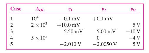
Data in the following table were taken for several op-amps operating in the open-loop configuration. Determine the unknown variables in the table. Case AOL V1 V2 1 104 -0.1 mV +0.1 mV 2345 2 x 10 +10.0 mV 5 V 5.50 mV 5.00 mV -10 V 5 x 10 0 -4 V -2.010 V -2.0050 V 5 V
(a) An inverting amplifier with resistors \(R_{1}=5.6 \mathrm{k} \Omega\) and \(R_{2}=120 \mathrm{k} \Omega\) is fabricated using an op-amp with an open-loop gain of \(10^{5}\). What is the percent difference between the actual gain and the ideal gain?(b) Repeat part (a) if \(R_{1}\) is changed to
(a) Consider a noniverting amplifier with \(R_{1}=6.8 \mathrm{k} \Omega, R_{2}=47 \mathrm{k} \Omega\), and an op-amp with \(A_{O L}=2 \times 10^{4}\). (i) What is the closed-loop gain? (ii) Determine the percent difference between the actual gain and the ideal gain.(b) Repeat part (a) if \(A_{O
(a) An op-amp is ideal except it has a finite open-loop gain of \(A_{O L}=2 \times 10^{3}\). The op-amp is connected in an inverting configuration. Determine \(R_{2} / R_{1}\) such that the closed-loop voltage gain is \(A_{C L}=-15.0\). (b) Using the results of part (a), what is the closed-loop
A noninverting amplifier is to be fabricated with a specification of an ideal closed-loop gain of 90 . What is the minimum open-loop gain of the opamp such that the closed-loop gain is within 0.01 percent of the ideal value?
The output of a voltage follower is to be within 0.02 percent of the ideal value. What is the minimum op-amp open-loop gain that is required?
An inverting amplifier is fabricated using 0.1 percent precision resistors. The nominal resistor values are \(R_{2}=210 \mathrm{k} \Omega\) and \(R_{1}=21.0 \mathrm{k} \Omega\).(a) If the op-amp is ideal, what is the range in the magnitude of voltage gain as a result of the variation in resistor
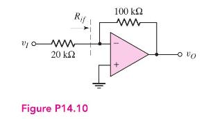
For the op-amp used in the inverting amplifier configuration in Figure P14.10, the open-loop parameters are \(A_{O L}=10^{3}\) and \(R_{o}=0\). Determine the closed- loop gain \(A_{C L}=v_{O} / v_{I}\) and input resistance \(R_{i f}\) for an openloop input differential-mode resistance of: (a)
A pressure transducer, as described in Example 14.1, is to be used in conjunction with a noninverting op-amp circuit. The ideal output voltage is to be +0.10 \(\mathrm{V}\) for a transducer voltage of \(2 \mathrm{mV}\). Determine the minimum open-loop gain required so that the actual output voltage
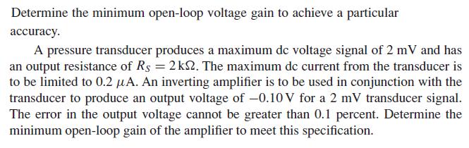
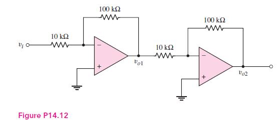
Consider the two inverting amplifiers in cascade in Figure P14.12. The opamp parameters are \(A_{O L}=5 \times 10^{3}, R_{i}=10 \mathrm{k} \Omega\), and \(R_{o}=1 \mathrm{k} \Omega\). Determine the actual closed-loop gains \(A_{v f 1}=v_{o 1} / v_{i}\) and \(A_{v f}=v_{o 2} / v_{i}\). What is the
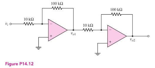
The noninverting amplifier in Figure P14.13 has an op-amp with open-loop properties: \(A_{O L}=10^{3}, R_{i}=20 \mathrm{k} \Omega\), and \(R_{o}=0.5 \mathrm{k} \Omega\). (a) Determine the closed-loop values of \(A_{C L}=v_{O} / v_{I}, R_{i f}\), and \(R_{o f}\). (b) If \(A_{O L}\) decreases by 10
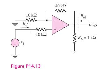
For the op-amp in the voltage follower circuit in Figure P14.14, the openloop parameters are \(A_{O L}=5 \times 10^{3}, R_{i}=10 \mathrm{k} \Omega\), and \(R_{o}=1 \mathrm{k} \Omega\). (a) Sketch the small-signal equivalent circuit. (b) Determine the (i) closed-loop voltage gain \(v_{O} / v_{I}\)
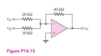
The summing amplifier in Figure P14.15 has an op-amp with open-loop parameters: \(A_{O L}=2 \times 10^{3}, R_{i}=\infty\), and \(R_{o}=0\). Determine the actual output voltage as a function of \(v_{I 1}\) and \(v_{I 2}\). What is the percent error from the ideal value? 20 www 10 + 40 ww Figure
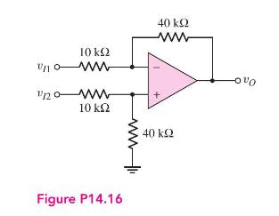
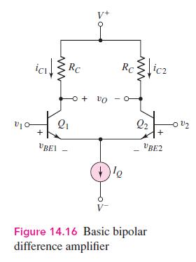
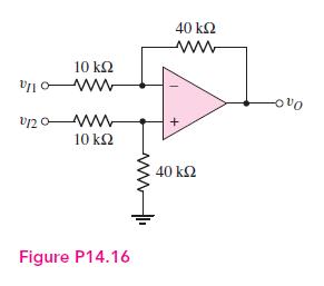
For the op-amp in the differential amplifier in Figure P14.16, the open-loop parameters are: \(A_{O L}=10^{3}, R_{i}=\infty\), and \(R_{o}=0\). Determine the actual differential voltage gain \(A_{d}=v_{O} /\left(v_{I 2}-v_{I 1}\right)\). What is the percentage error from the ideal value? 10 ww 40
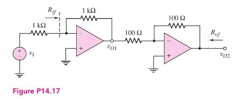
Because of a manufacturing error, the open-loop gain of each op-amp in the circuit in Figure P14.17 is only \(A_{O L}=100\). The open-loop input and output resistances are \(R_{i}=10 \mathrm{k} \Omega\) and \(R_{o}=1 \mathrm{k} \Omega\), respectively. Determine the closed-loop parameters: (a)
An inverting amplifier has a closed-loop voltage gain of -25 . The op-amp used has a low-frequency, open-loop gain of \(2 \times 10^{4}\) and has a unity-gain bandwidth of \(10^{6} \mathrm{~Hz}\). (a) What is the \(3 \mathrm{~dB}\) frequency \(f_{3 \text {-dB }}\) of the op-amp and the \(3
The open-loop low-frequency gain of an op-amp is \(A_{o}=100 \mathrm{~dB}\). At a frequency of \(f=10^{4} \mathrm{~Hz}\), the magnitude of the open-loop gain is \(38 \mathrm{~dB}\). Determine the dominant-pole frequency and the unity gain bandwidth.
A noninverting amplifier uses 5 percent precision resistors with nominal values of \(R_{2}=150 \mathrm{k} \Omega\) and \(R_{1}=15 \mathrm{k} \Omega\). The op-amp has a low-frequency gain of \(A_{o}=3 \times 10^{4}\) and has a unity-gain bandwidth of \(f_{T}=1.2 \mathrm{MHz}\). (a) What is the
The low-frequency open-loop gain of an op-amp is \(2 \times 10^{5}\) and the second pole occurs at a frequency of \(5 \mathrm{MHz}\). An amplifier using this op-amp has a low-frequency closed-loop gain of 100 and a phase margin of 80 degrees. Determine the dominant-pole frequency.
Two inverting amplifiers are connected in cascade to provide an overall voltage gain of 500 . The gain of the first amplifier is -10 and the gain of the second amplifier is -50 . The unity-gain bandwidth of each op-amp is \(1 \mathrm{MHz}\). (a) What is the bandwidth of the overall amplifier
Three inverting amplifiers, each with \(R_{2}=150 \mathrm{k} \Omega\) and \(R_{1}=15 \mathrm{k} \Omega\), are connected in cascade. Each op-amp has a low-frequency gain of \(A_{o}=5 \times 10^{4}\) and a unity-gain bandwidth of \(f_{T}=1.5 \mathrm{MHz}\). (a) Determine the low-frequency closed-loop
An inverting amplifier circuit has a voltage gain of -25 . The op-amp used in the circuit has a low-frequency voltage gain of \(5 \times 10^{4}\) and a unity-gain bandwidth of \(1 \mathrm{MHz}\). Determine the dominant pole frequency of the opamp and the small-signal bandwidth,
An audio amplifier system, using a noninverting op-amp circuit, needs to have a small-signal bandwidth of \(20 \mathrm{kHz}\). The open-loop low-frequency voltage gain of the op-amp is \(10^{5}\) and the unity-gain bandwidth is \(1 \mathrm{MHz}\). What is the maximum closed-loop voltage gain that
If an op-amp has a slew-rate of \(5 \mathrm{~V} / \mu \mathrm{s}\), find the full-power bandwidth for a peak output voltage of (a) \(5 \mathrm{~V}\), (b) \(1.5 \mathrm{~V}\), and (c) \(0.4 \mathrm{~V}\).
(a) An op-amp with a slew rate of \(8 \mathrm{~V} / \mu \mathrm{s}\) is driven by a \(250 \mathrm{kHz}\) sine wave. What is the maximum output amplitude at which slew-rate limiting is reached?(b) Repeat part (a) for a \(250 \mathrm{kHz}\) zero time-average triangular wave.
An amplifier system is to be designed to provide an undistorted \(10 \mathrm{~V}\) peak sinusoidal signal at a frequency of \(f=12 \mathrm{kHz}\). Determine the minimum slew rate required for the amplifier.
(a) The op-amp to be used in the audio amplifier system in Problem 14.25 has a slew rate of \(0.63 \mathrm{~V} / \mu \mathrm{s}\). Determine the peak value of undistorted output voltage that can be achieved.(b) Repeat part (a) if the slew rate is \(3 \mathrm{~V} / \mu \mathrm{s}\).Data From Problem
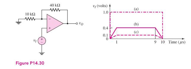
The op-amp in the noninverting amplifier configuration in Figure P14.30 has a slew rate of \(1 \mathrm{~V} / \mu \mathrm{s}\). Sketch the output voltage versus time for each of the three inputs shown. The op-amp is biased at \(\pm 10 \mathrm{~V}\). 10 ww 40 ww Figure P14.30 v (volts) (a) 1.0 (b)
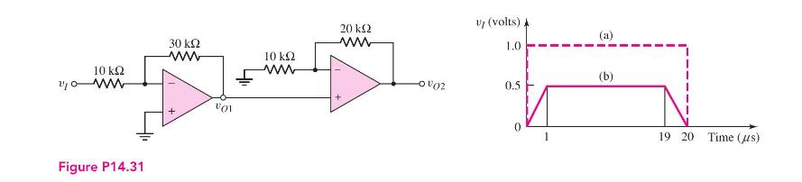
For each op-amp in the circuit shown in Figure P14.31, the bias is \(\pm 15 \mathrm{~V}\) and the slew rate is \(3 \mathrm{~V} / \mu \mathrm{s}\). Sketch the output voltages \(v_{O 1}\) and \(v_{O 2}\) versus time for each input shown. 10 WWW 30 www 10 www 20 www Figure P14.31 Uj (volts) 1.0
For the transistors in the diff-amp in Figure 14.16 in the text, the current parameters \(I_{S 1}\) and \(I_{S 2}\) can be written as \(5 \times 10^{-14}(1+x)\) A, where \(x\) represents the deviation from the ideal due to variations in electrical and geometric characteristics. (The value of \(x\)
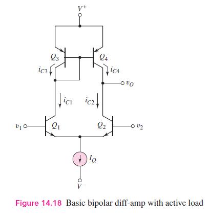
The bipolar active load diff-amp in Figure 14.18 is biased at \(V^{+}=5 \mathrm{~V}\) and \(V^{-}=-5 \mathrm{~V}\). The transistor parameters are \(V_{A N}=120 \mathrm{~V}, V_{A P}=80 \mathrm{~V}\), \(v_{B E}(\mathrm{npn})=v_{E B}(\mathrm{pnp})=0.6 \mathrm{~V}, I_{S 1}=I_{S 2}\), and \(I_{S 3}=5
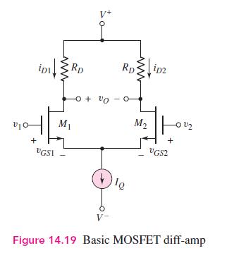
For the transistors in the diff-amp in Figure 14.19, the conduction parameters can be written as \(150(1+x) \mu \mathrm{A} / \mathrm{V}^{2}\), where \(x\) represents the deviation from the ideal due to variations in electrical and geometric characteristics. (The value of \(x\) is positive for one
(a) An inverting op-amp circuit has a gain of -30. The op-amp used in the circuit has an offset voltage of \(\pm 2 \mathrm{mV}\). If the input signal voltage to the amplifier is \(10 \mathrm{mV}\), determine the possible range in the output voltage.(b) Repeat part (a) if the input signal voltage is
Repeat Problem 14.35 for an input signal voltage of \(v_{I}=25 \sin \omega t(\mathrm{mV})\).Data From Problem 14.35:-(a) An inverting op-amp circuit has a gain of -30. The op-amp used in the circuit has an offset voltage of \(\pm 2 \mathrm{mV}\). If the input signal voltage to the amplifier is \(10
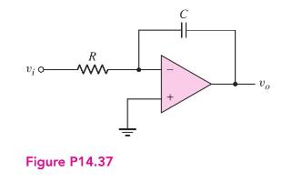
Consider the integrator circuit in Figure P14.37. The circuit parameters are \(R=10 \mathrm{k} \Omega\) and \(C=10 \mu \mathrm{F}\). The op-amp offset voltage is \(\pm 5 \mathrm{mV}\). For \(v_{i}=0\), determine the output voltage versus time. For the worst-case offset voltage, determine the time
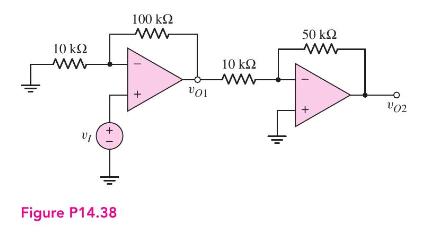
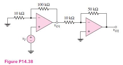
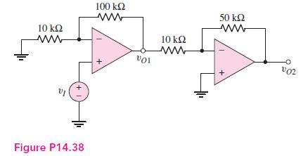
In the circuit in Figure P14.38, the offset voltage of each op-amp is \(\pm 3 \mathrm{mV}\).(a) Determine the possible range in output voltages \(v_{O 1}\) and \(v_{O 2}\) for \(v_{I}=0\).(b) Repeat part (a) for \(v_{I}=10 \mathrm{mV}\).(c) Repeat part (a) for \(v_{I}=100 \mathrm{mV}\).(d) Design
In the circuit shown in Figure P14.39, the op-amp is ideal. For \(v_{I}=0.5 \mathrm{~V}\), determine \(v_{O}\) when the wiper arm of the potentiometer is at the \(V^{+}\)node, in the center, and at the \(V^{-}\)node.Figure P14.39:- R = 10 k
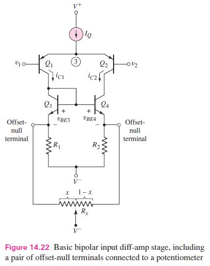
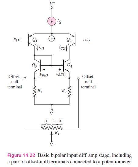
Consider the bipolar diff-amp with an active load and a pair of offset-null terminals as shown in Figure 14.22 in the text. Let \(R_{1}=R_{2}=500 \Omega\) and let \(R_{x}\) be a \(50 \mathrm{k} \Omega\) potentiometer. (a) If the wiper arm of the potentiometer is exactly in the center, determine the
The bipolar diff-amp in Figure 14.22 in the text is biased at \(I_{Q}=500 \mu \mathrm{A}\). Assume all transistors are matched, with \(I_{S}=10^{-14} \mathrm{~A}\). Let \(R_{1}=R_{2}=\) \(500 \Omega\), and assume \(R_{x}\) is a \(50 \mathrm{k} \Omega\) potentiometer. If the wiper arm of the
(a) An op-amp is connected in an inverting amplifier configuration with \(R_{2}=200 \mathrm{k} \Omega\) and \(R_{1}=20 \mathrm{k} \Omega\). The input bias current at the inverting terminal is \(1 \mu \mathrm{A}\) and the input bias current at the noninverting terminal is \(2 \mu \mathrm{A}\).
An inverting amplifier has parameters \(R_{2}=150 \mathrm{k} \Omega\) and \(R_{1}=15 \mathrm{k} \Omega\). Bias currents of \(2 \mu \mathrm{A}\) are leaving each op-amp terminal. Determine the output voltage if the input voltage is (a) \(v_{I}=0\), (b) \(v_{I}=20 \mathrm{mV}\), (c) \(v_{I}=-20
An op-amp is connected in a noninverting amplifier configuration with a voltage gain of +41 . The feedback resistor is \(250 \mathrm{k} \Omega\). The op-amp has input bias currents of \(I_{B 1}=I_{B 2}=0.6 \mu \mathrm{A}\). Determine the output voltage \(v_{O}\) for input voltages of (a)
An op-amp used in a voltage follower configuration is ideal except that the input bias currents are \(I_{B 1}=I_{B 2}=1 \mu \mathrm{A}\). The source driving the voltage follower has an output resistance of \(10 \mathrm{k} \Omega\). (a) Find the output voltage due to the bias current effects when
In the differential amplifier in Figure P14.16, the op-amp is ideal except that the average input bias current is \(I_{B}=10 \mu \mathrm{A}\) and the input offset current is \(I_{O S}=3 \mu \mathrm{A}\). If \(v_{i 1}=v_{i 2}=0\), determine the worst-case output voltage \(v_{O}\) due to the input
The op-amp bias currents for the circuit in Figure P14.38 are equal at \(I_{B 1}=\) \(I_{B 2}=1 \mu \mathrm{A}\). (a) Find the worst-case output voltages \(v_{O 1}\) and \(v_{O 2}\) for \(v_{I}=0\). (b) Design input bias current compensation circuit(s) to adjust both \(v_{O 1}\) and \(v_{O 2}\) to
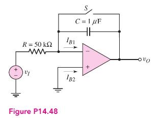
(a) For the integrator circuit in Figure P14.48, let the input bias currents be \(I_{B 1}=I_{B 2}=0.1 \mu \mathrm{A}\). Assume that switch \(S\) opens at \(t=0\). Derive an expression for the output voltage versus time for \(v_{I}=0\).(b) Plot \(v_{O}\) versus time for \(0 \leq t \leq 10
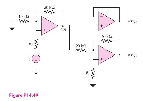
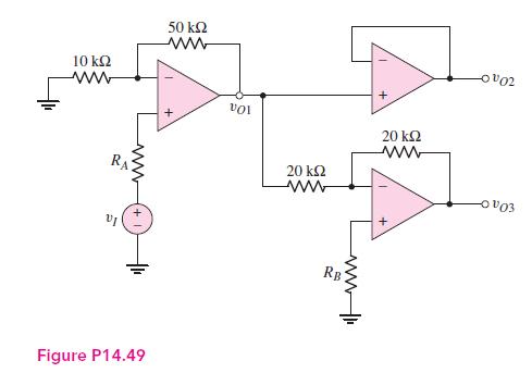
For the circuit in Figure P14.49, the op-amps are ideal except that the opamps have bias currents of \(I_{B}=3 \mu \mathrm{A}\) entering each op-amp terminal. (a) For \(v_{I}=0\) and \(R_{A}=R_{B}=0\), determine the values of \(v_{O 1}, v_{O 2}\), and \(v_{O 3}\). (b) Determine the values of
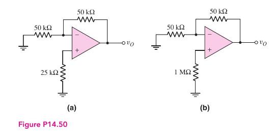
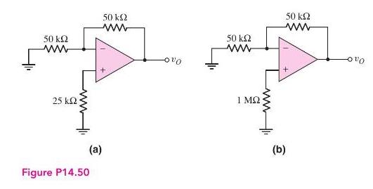
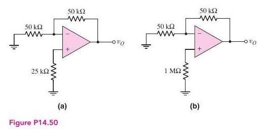
For each circuit in Figure P14.50, the input bias current is \(I_{B}=0.8 \mu \mathrm{A}\) the input offset current is \(I_{O S}=0.2 \mu \mathrm{A}\). (a) Determine the output voltage due to the average bias current \(I_{B}\). (b) Determine the worst-case output voltage, including the effect of the
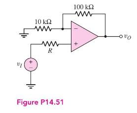
For the op-amp in Figure P14.51, the input offset voltage is \(V_{O S}=3 \mathrm{mV}\), the average input bias current is \(I_{B}=0.4 \mu \mathrm{A}\), and the offset bias current is \(I_{O S}=0.06 \mu \mathrm{A}\).(a) Determine the possible range in output voltage for \(v_{I}=0\) and \(R=0\).(b)
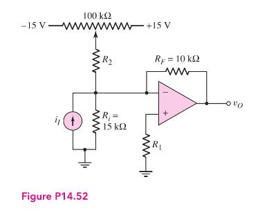
Consider the op-amp circuit in Figure P14.52. (a) Find the value of \(R_{2}\) needed for \(\mathrm{a} \pm 10 \mathrm{mV}\) offset voltage adjustment. (b) Determine \(R_{1}\) to minimize bias current effects. (Assume \(R_{2} \gg R_{i}\).) 100 k2 -15 v-www wwww+15 V R Rp = 10 k www R = 15 Figure
For each op-amp in the circuit in Figure P14.38, the offset voltage is \(V_{O S}=10 \mathrm{mV}\) and the input bias currents are \(I_{B 1}=I_{B 2}=2 \mu \mathrm{A}\). (a) Find the worst-case output voltages \(v_{O 1}\) and \(v_{O 2}\) for \(v_{I}=0\). (b) Design compensation circuits to adjust
The op-amps in the circuit in Figure P14.49 have an offset voltage \(V_{O S}=2 \mathrm{mV}\), an average input bias current of \(I_{B}=0.2 \mu \mathrm{A}\), and an offset current of \(I_{O S}=0.02 \mu \mathrm{A}\).(a) For \(v_{I}=0\) and \(R_{A}=R_{B}=0\), determine the possible range in output
Each op-amp in Figure P14.50 has an offset voltage of \(V_{O S}=2 \mathrm{mV}\), an average input bias current of \(I_{B}=500 \mathrm{nA}\), and an input offset current of \(I_{O S}=100 \mathrm{nA}\). Determine the worst-case output voltage for each circuit. 50 ww 50 ww 50 www 50 ww 25 ww
For each op-amp in Figure P14.50, the input offset voltage is \(V_{O S}=2 \mathrm{mV}\) at \(T=25^{\circ} \mathrm{C}\) and the input offset voltage temperature coefficient is \(\mathrm{TC} v_{O S}=6.7 \mu \mathrm{V} /{ }^{\circ} \mathrm{C}\). Find the output voltage \(v_{O}\) due to the input
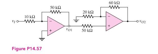
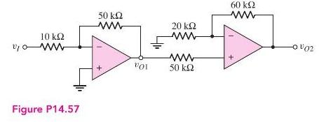
The input offset voltage in each op-amp in Figure P14.57 is \(V_{O S}=1 \mathrm{mV}\) at \(T=25^{\circ} \mathrm{C}\) and the input offset voltage coefficient is \(\mathrm{TC} v_{O S}=3.3 \mu \mathrm{V} /{ }^{\circ} \mathrm{C}\). Find the worst-case output voltages \(v_{O 1}\) and \(v_{O 2}\) at:
For each op-amp in Figure P14.50, the input bias current is \(I_{B}=500 \mathrm{nA}\) at \(T=25^{\circ} \mathrm{C}\), the input offset current is \(I_{O S}=200 \mathrm{nA}\) at \(T=25^{\circ} \mathrm{C}\), the input bias current temperature coefficient is \(8 \mathrm{nA} /{ }^{\circ} \mathrm{C}\),
For each op-amp in Figure P14.57, the input bias current is \(I_{B}=2 \mu \mathrm{A}\) at \(T=25^{\circ} \mathrm{C}\), the input offset current is \(I_{O S}=0.2 \mu \mathrm{A}\) at \(T=25^{\circ} \mathrm{C}\), the input bias current temperature coefficient is \(20 \mathrm{nA} /{ }^{\circ}
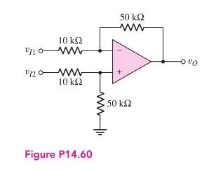
The op-amp in the difference amplifier configuration in Figure P14.60 is ideal.(a) If the tolerance of each resistor is \(\pm 1.5 \%\), determine the minimum value of \(\mathrm{CMRR}_{\mathrm{dB}}\).(b) Repeat part (a) if the tolerance of each resistor is \(\pm 3 \%\). 50 ww 1 0- 10 ww 120 ww 10
If the tolerance of each resistor in the difference amplifier in Figure P14.60 is \(\pm x \%\), what is the maximum value of \(x\) if the minimum \(\mathrm{CMRR}_{\mathrm{dB}}\) is (a) \(50 \mathrm{~dB}\) and (b) \(75 \mathrm{~dB}\). 50 ww 1 0- 10 ww 120 ww 10 50 Figure P14.60
Consider an inverting amplifier such as shown in Figure 14.2. Bias a standard op-amp at \(\pm 5 \mathrm{~V}\), and let \(R_{2}=100 \mathrm{k} \Omega\) and \(R_{1}=10 \mathrm{k} \Omega\). Using a computer simulation, plot \(v_{O}\) versus \(v_{I}\) over the range \(-0.7 \leq v_{I} \leq 0.7
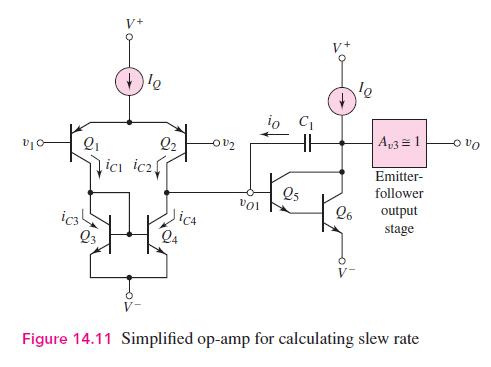
Consider the simplified op-amp shown in Figure 14.11. Use standard transistors and take the output at the collector of \(Q_{6}\). Assume the bias current for \(Q_{1}\) and \(Q_{2}\) is \(I_{Q}=19 \mu \mathrm{A}\) and the bias current for \(Q_{5}\) and \(Q_{6}\) is \(I_{Q}=0.15 \mathrm{~mA}\). Let
The equivalent circuit of the all-CMOS MC14573 op-amp was given in Figure 13.14. Using a computer simulation, determine the slew rate of the op-amp assuming \(C_{1}=12 \mathrm{pF}\). Use standard transistors. M5 M6 Mg Wo M C set M3 M4 M Figure 13.14 MC14573 CMOS op-amp equivalent circuit
A basic bipolar input diff-amp stage is shown in Figure 14.22. Use standard transistors and other appropriate circuit parameters. Let \(v_{1}=v_{2}=0\). (a) Plot \(i_{C 1}\) and \(i_{C 2}\) as a function of the wiper arm position \(x\). (b) Plot the collector voltage of \(Q_{4}\) as a function of
An amplifier system, using op-amps, is to be designed to provide a lowfrequency voltage gain of 50 and a bandwidth of \(20 \mathrm{kHz}\). The only available op-amps have a low-frequency open-loop voltage gain of \(3 \times 10^{4}\) and a bandwidth of \(10 \mathrm{~Hz}\). Design an appropriate
Consider the simplified op-amp in Figure 14.11. Neglect the emitter-follower output stage. Assume bias voltages of \(V^{+}=3 \mathrm{~V}\) and \(V^{-}=-3 V\). Let the bias current for \(Q_{5}\) and \(Q_{6}\) be \(I_{Q}=0.1 \mathrm{~mA}\). The total power dissipated in the circuit is to be limited
Consider the op-amp circuit shown in Figure P14.12. Each op-amp has an offset voltage of \(V_{O S}=2 \mathrm{mV}\). Design an offset voltage compensation circuit. Assume bias voltages are limited to \(\pm 5 \mathrm{~V}\). V; 0- 10 ww Figure P14.12 100 www Vol 10 www 100 www 002
Consider the op-amp circuit shown in Figure P14.12. Each op-amp has an average input bias current of \(I_{B}=1 \mu \mathrm{A}\) and the offset bias current is \(I_{O S}=0.1 \mu \mathrm{A}\). Design an optimum bias-current compensation circuit. What is the possible range of output voltage \(v_{O
(a) A negative-feedback amplifier has a closed-loop gain of \(A_{f}=100\) and an open-loop gain of \(A=5 \times 10^{4}\). Determine the feedback transfer function \(\beta\). (b) If \(\beta=0.012\) and \(A_{f}=80\), determine the open-loop gain \(A\).
(a) The closed-loop gain of a negative-feedback amplifier is \(A_{f}=-80\) and the open-loop gain is \(A=-10^{5}\). Find the feedback transfer function \(\beta\). (b) If \(\beta=-0.015\) and \(A=-5 \times 10^{4}\), determine the closed-loop gain \(A_{f}\).
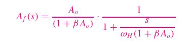
The ideal feedback transfer function is given by Equation (12.5).(a) Assume the feedback transfer function is \(\beta=0.15\). Determine the loop gain \(T\) and the closed-loop gain \(A_{f}\) for (i) \(A=\infty\), (ii) \(A=80 \mathrm{~dB}\), and (c) \(A=10^{2}\).(b) Repeat part (a) for
(a) The closed-loop gain of a feedback amplifier using an ideal feedback amplifier \((A \rightarrow \infty)\) is \(A_{f}=125\). What is the value of \(\beta\) ? (b) If the basic amplifier has a finite open-loop gain, what must be the value of \(A\) such that the closed-loop gain is within 0.25
Consider the feedback system shown in Figure 12.1. The closed-loop gain is \(A_{f}=-80\) and the open-loop gain is \(A=-2 \times 10^{4}\). (a) Determine the feedback transfer function \(\beta\). (b) The closed-loop gain is not to change by more than 0.01 percent when the open-loop gain changes.
The open-loop gain of an amplifier is \(A=5 \times 10^{4}\). If the open-loop gain decreases by 10 percent, the closed-loop gain must not change by more than 0.1 percent. Determine the required value of the feedback transfer function \(\beta\) and the closed-loop gain \(A_{f}\).
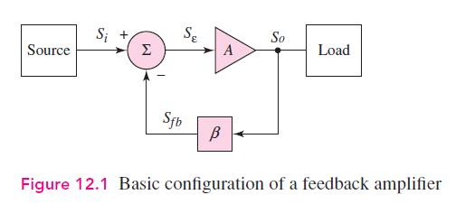
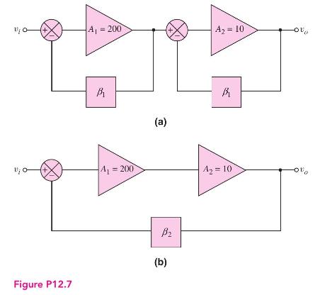
Two feedback configurations are shown in Figures P12.7(a) and P12.7(b). The closed-loop gain in each case is \(A_{v f}=v_{o} / v_{i}=50\).(a) Determine \(\beta_{1}\) and \(\beta_{2}\) for the two circuits.(b) The gain \(A_{2}\) decreases by 10 percent in both circuits. Using the results of part
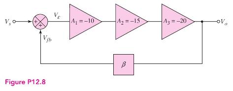
Three voltage amplifiers are in cascade as shown in Figure P12.8 with various amplification factors. The 180 degree phase shift for negative feedback actually occurs in the basic amplifier itself. (a) Determine the value of \(\beta\) such that the closed-loop voltage gain is \(A_{v f}=V_{o} /
(a) The open-loop low-frequency voltage gain of an amplifier is \(A_{v}=\) \(5 \times 10^{4}\) and the open-loop \(3 \mathrm{~dB}\) frequency is \(f_{H}=10 \mathrm{~Hz}\). If the closed-loop low-frequency gain is \(A_{v f}=25\), what is the closed-loop bandwidth? (b) The minimum closed-loop
(a) Determine the closed-loop bandwidth of a noninverting amplifier with a closed-loop low-frequency gain of 50. The op-amp has the characteristics described in Problem 12.9(a). (b) If the open-loop gain decreases to \(A_{v}=10^{4}\) but the closed-loop low-frequency gain remains fixed at 50, what
(a) An inverting amplifier uses an op-amp with an open-loop \(3 \mathrm{~dB}\) frequency of \(5 \mathrm{~Hz}\). The closed-loop low-frequency gain is to be \(\left|A_{v f}\right|=75\) and the closed-loop bandwidth is to be \(35 \mathrm{kHz}\). (i) What is the required value of the open-loop
The basic amplifier in a feedback configuration has a low-frequency gain of \(A=5000\) and two pole frequencies at \(f_{3-\mathrm{dB} 1}=10 \mathrm{~Hz}\) and \(f_{3-\mathrm{dB} 2}=2 \mathrm{kHz}\). The low-frequency closed-loop gain is \(A_{f}=100\). Determine the two \(3 \mathrm{~dB}\)
Showing 400 - 500
of 4723
1
2
3
4
5
6
7
8
9
10
11
12
13
14
15
Last
Step by Step Answers