New Semester
Started
Get
50% OFF
Study Help!
--h --m --s
Claim Now
Question Answers
Textbooks
Find textbooks, questions and answers
Oops, something went wrong!
Change your search query and then try again
S
Books
FREE
Study Help
Expert Questions
Accounting
General Management
Mathematics
Finance
Organizational Behaviour
Law
Physics
Operating System
Management Leadership
Sociology
Programming
Marketing
Database
Computer Network
Economics
Textbooks Solutions
Accounting
Managerial Accounting
Management Leadership
Cost Accounting
Statistics
Business Law
Corporate Finance
Finance
Economics
Auditing
Tutors
Online Tutors
Find a Tutor
Hire a Tutor
Become a Tutor
AI Tutor
AI Study Planner
NEW
Sell Books
Search
Search
Sign In
Register
study help
computer science
digital systems principles and application
Digital Systems Principles And Application 12th Edition Ronald Tocci, Neal Widmer, Gregory Moss - Solutions
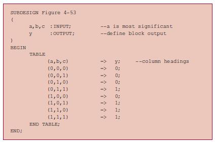
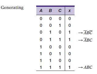
Modify the AHDL truth table of Figure 4-53 to implement AB + AC̅ + A̅B.Figure 4-53 SUBDESIGN Figure 4-53 ( :) BEGIN END; a, b,c : INPUT; y : OUTPUT; TABLE (a,b,c) (0,0,0) (0,0,1) (0,1,0) (0,1,1) (1,0,0) (1,0,1) (1,1,0) (1,1,1) END TABLE; --a is most significant --define block output ->
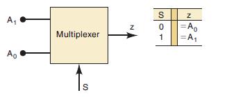
Design a logic circuit that has two signal inputs, A1 and A0, and a control input S so that it functions according to the requirements given in Figure 4-78. (This type of circuit is called a multiplexer and will be covered in Chapter 9.)Figure 4-78 A₁ Ao Multiplexer S Z S01 S N |=A₂ =A₁
Use K mapping to design a circuit to meet the requirements of Example 4-17. Compare this circuit with the solution in Figure 4-23. This points out that the K-map method cannot take advantage of the XOR and XNOR gate logic. The designer must be able to determine when these gates are
(a) A technician testing a logic circuit sees that the output of a particular INVERTER is stuck LOW while its input is pulsing. List as many possible reasons as you can for this faulty operation.(b) Repeat part (a) for the case where the INVERTER output is stuck at an indeterminate logic level.
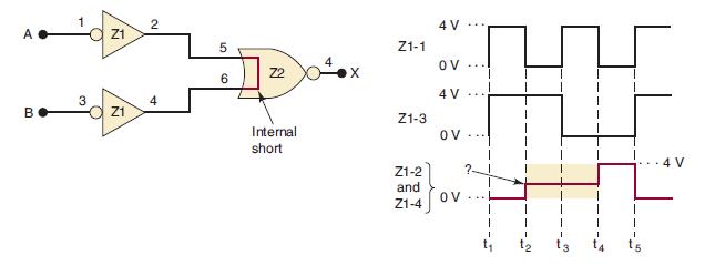
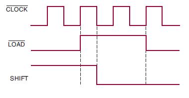
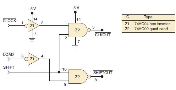
The signals shown in Figure 4-79 are applied to the inputs of the circuit of Figure 4-32. Suppose that there is an internal open circuit at Z1-4.(a) What will a logic probe indicate at Z1-4?(b) What dc voltage reading would you expect at Z1-4? (Remember that the ICs are TTL.)Figure 4-79Figure 4-32
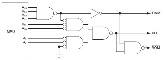
In some microcomputers, the MPU can be disabled for short periods of time while another device controls the RAM, ROM, and I/O. During these intervals, a special control signal (D̅M̅A̅) is activated by the MPU and is used to disable (deactivate) the device select logic so that theare all in their
In a microcomputer, the microprocessor unit (MPU) is always communicating with one of the following: (1) Random-access memory (RAM), which stores programs and data that can be readily changed; (2) Read only memory (ROM), which stores programs and data that never change; (3) External input/output
Define each of the following terms.(a) Karnaugh map(b) Sum-of-products form(c) Parity generator(d) Octet(e) Enable circuit(f) Don’t-care condition(g) Floating input(h) Indeterminate voltage level(i) Contention(j) PLD(k) TTL(l) CMOS
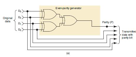
Write the hardware description design file Boolean equation to implement a four-bit parity generator as shown in Figure 4-25(a).Figure 4-25(a) Š Original D₂ data P D₁ Do > 8 Even-parity generator B D (a) Parity (P) Transmitted data with parity bit
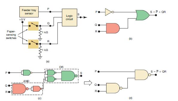
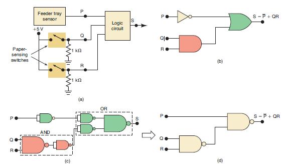
Write the hardware description design file Boolean equation to implement Example 4-9.Data from Example 4-9Refer to Figure 4-9(a). In a simple copy machine, a stop signal, S, is to be generated to stop the machine operation and energize an indicator light whenever either of the following conditions
Modify (a) The AHDL design in Figure 4-63 to implement Table 4-1.(b) The VHDL design in Figure 4-64 to implement Table 4-1.Figure 4-63Table 4-1 SUBDESIGN Figure 4-63 ( ) P, q, r S VARIABLE status [2..0] BEGIN END CASE; : INPUT; :OUTPUT; END; :NODE; status] (p, q, r); -- link input bits in
Modify the AHDL design in Figure 4-57 so that z = 1 only when the digital value is less than 10102.Figure 4-57 SUBDESIGN Figure 4-57 digital_value [3..0] ( Z BEGIN IF digital value [] > 6 THEN z = VCC; ELSE z = GND; END IF: : INPUT; : OUTPUT; END; -- -- -- define inputs to block define block
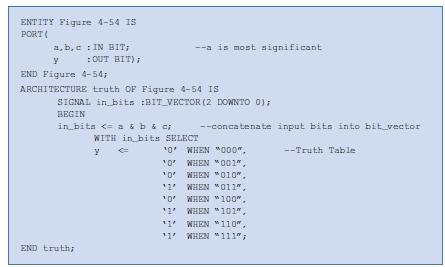
Modify the VHDL truth table of Figure 4-54 to implement AB + AC̅ + A̅B.Figure 4-54 ENTITY Figure 4-54 IS PORT( a,b,c IN BIT; y END Figure 4-54; : OUT BIT); ARCHITECTURE truth OF Figure 4-54 IS SIGNAL in bits :BIT VECTOR (2 DOWNTO 0); BEGIN in bits
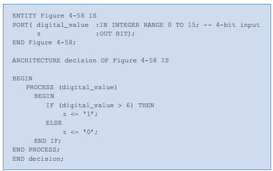
Modify the code of (a) Figure 4-57 Figure 4-57(b) Figure 4-58 such that the output z is LOW only when digital_value is between 6 and 11 (inclusive).Figure 4-58 SUBDESIGN Figure 4-57 digital value [ 3..0] ( Z ) BEGIN IF digital_value [] > 6 THEN z = VCC; ELSE Z = GND; END IF; : INPUT; :
How many XOR gates are required to generate the parity bit for an eight-bit data value?
Design a logic circuit with three inputs A, B, C and an output that goes LOW only when A is HIGH while B and C are different.
Which type of transistor is used in (a) TTL (b) CMOS?
What is the unique state of an AND gate output?
List the three steps necessary to recover from a system fault or failure.
List the different internal digital IC faults.
What is actually being “programmed” in a PLD?
What are the most common types of external faults?
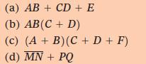
Which of the following expressions is in SOP form? (a) AB + CD + E (b) AB (C + D) (c) (A + B) (C + D + F) (d) MN + PQ
How would you declare a six-bit input array named push_buttons in(a) AHDL (b) VHDL?
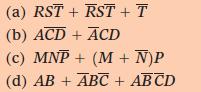
State which of the following expressions are not in the sum-of-products form: (a) RST + RST + T (b) ACD + ACD (c) MNP+ (M + N)P (d) AB + ABC + AB CD
List two advantages of simplification.
How would you concatenate three bits x, y, and z into a three-bit array named omega? Use AHDL or VHDL.
Which control structure decides to do or not to do?
Write the sum-of-products expression for a circuit with four inputs and an output that is to be HIGH only when input A is LOW at the same time that exactly two other inputs are LOW.
Use K mapping to obtain the expression of Example 4-7.Example 4-7Design a logic circuit that has three inputs, A, B, and C, and whose output will be HIGH only when a majority of the inputs are HIGH.
Use Boolean algebra to prove that the XNOR output expression is the exact inverse of the XOR output expression.
How many XOR gates are required to check the parity bit for an eight-bit data value (plus one parity bit)?
Design a circuit to pass signal A only when B is HIGH and C is LOW. The output must be LOW when A is not being passed.
Name the six common categories of digital ICs according to complexity.
If the output of an AND gate is not in its unique state, but should be, what is the most likely problem?
List the indicators on a logic probe.
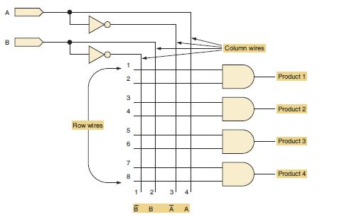
What bits (column, row) in Figure 4-44 must be connected to make Product 1 = AB?Figure 4-44 A B 00 Row wires 2 3 5 6 78 2 В В 3 14 A A Column wires Product 1 Product 2 Product 3 Product 4
Which internal IC fault can produce signals that show three different voltage levels?
List some of the causes of signal-path open circuits.
What statement would you use to take the MSB from the array in question 1 and put it on a single-bit output port named z? Use (a) AHDL(b) VHDL.
Repeat question 1 for the POS form.Data from Question 1Which of the following expressions is in SOP form? (a) AB + CD + E (b) AB (C + D) (c) (A + B) (C + D + F) (d) MN + PQ
List two methods of simplification.
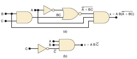
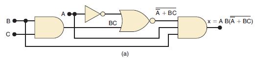
Simplify the circuit in Figure 4-1(a) to arrive at the circuit of Figure 4-1(b).Figure 4-1 B O O A BC (a) (b) A + BC x=ABC x= A B(A + BC)
How are truth tables implemented in AHDL?
Which control structure decides to do this or to do that?
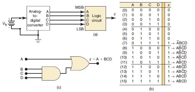
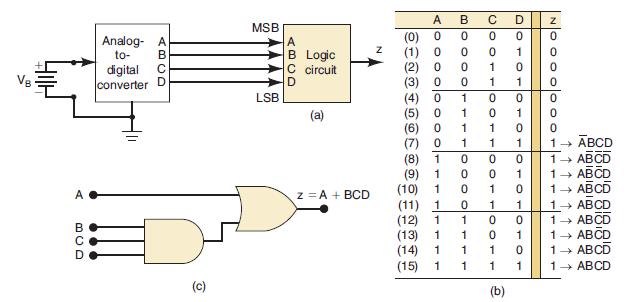
Use K mapping to obtain the expression of Example 4-8. This should emphasize the advantage of K mapping for expressions containing many terms.Data from Example 4-8Refer to Figure 4-8(a), where an analog-to-digital converter is monitoring the dc voltage (VB) of a 12-V storage battery on an orbiting
Implement the expression of question 1 using all four-input NAND gates. How many are required?Data from question 1Write the sum-of-products expression for a circuit with four inputs and an output that is to be HIGH only when input A is LOW at the same time that exactly two other inputs are LOW.
What is the output of an XNOR gate when a logic signal and its exact inverse are connected to its inputs?
Which logic gates produce a 1 output in the disabled state?
True or false: A 74S74 chip will contain the same logic and pin layout as the 74LS74.
What would a logic probe indicate at Z1-2 and Z1-4 of Figure 4-39 if A = 0 and B = 1?Figure 4-39 A B 3 Z1 Z1 2 4 5 6 Z2 Internal short Z1-1 Z1-3 Z1-2 and Z1-4 4 V OV 4 V OV OV ? T I I 1 4 V
What is the unique state of an OR gate output?
What bits (column, row) in Figure 4-44 must be connected to make Product 3 = AB̅?Figure 4-44 A B 00 Row wires 2 3 5 6 78 2 В В 3 14 A A Column wires Product 1 Product 2 Product 3 Product 4
What symptoms are caused by a faulty power supply?
Change each AND gate in Figure 4-1(a) to a NAND gate. Determine the new expression for x and simplify it.Figure 4-1(a) B C BC (a) A + BC x = A B(A + BC)
In VHDL, what is the IEEE standard type that is equivalent to the BIT type?
How are truth tables implemented in VHDL?
Which control structure(s) selects which one of several different actions to take?
Obtain the expression of Example 4-9 using a K map.Data from Example 9Refer to Figure 4-9(a). In a simple copy machine, a stop signal, S, is to be generated to stop the machine operation and energize an indicator light whenever either of the following conditions exists: (1) there is no paper in the
List the steps of the systematic design process.
A logic designer needs an INVERTER, and all that is available is one XOR gate from a 74HC86 chip. Does he need another chip?
Which logic gates pass the inverse of the input signal when they are enabled?
True or false: A 74HC74 chip will contain the same logic and pin layout as the 74AS74.
If the output of an OR gate is not in its unique state, but should be, what is the most likely problem?
What is signal contention?
Define hierarchical design.
How might loading affect an IC output voltage level?
In VHDL, what is the IEEE standard type that is equivalent to the BIT_VECTOR type?
True or false: IF/THEN/ELSE and CASE constructs must be used inside a process in VHDL.
What is a don’t-care condition?
Which CMOS series are not pin-compatible with TTL?
If a circuit node has the incorrect logic level, why would you test the other end of the wire that is supposed to drive that node?
Most modern PLDs are programmed in-circuit using the _______ standard interface.
List the number systems that can be used with AHDL and VHDL.
True or false: IF/THEN/ELSE constructs can be used throughout the concurrent section of AHDL.
What is the acceptable input voltage range of a logic 0 for TTL? What is it for a logic 1?
If you suspect an output is incorrect because of a loading problem (in thecircuit it is driving), how can you prove it?
Repeat question 6 for CMOS operating at VDD = 5 V.Data from Question 6What is the acceptable input voltage range of a logic 0 for TTL? What is it for a logic 1?
How does a TTL integrated circuit respond to a floating input?
How does a CMOS integrated circuit respond to a floating input?
Which CMOS series can be connected directly to TTL with no interfacing circuitry?
What is the purpose of pin numbers on a logic circuit connection diagram?
What are the key similarities of graphic design files used for programmable logic and traditional logic circuit connection diagrams?
The following English expression describes the way a logic circuit needs to operate in order to drive a seatbelt warning indicator in a car.if the driver is present aND the driver is NOT buckled up aND the ignition switch is on, THeN turn on the warning light.Describe the circuit using Boolean
Simplify the logic circuit shown in Figure 4-2(a).Figure 4-2(a) A C Ф B A AC A B C A B (a) AB(AC) z = ABC + AB(AC)
Simplify the expression z = AB̅ C̅ + AB̅C + ABC
Simplify the circuit of Figure 4-3(a).Figure 4-3 A B (a) A B 13 G Z
Simplify the expression x = (A̅ + B) (A + B + D)D̅.
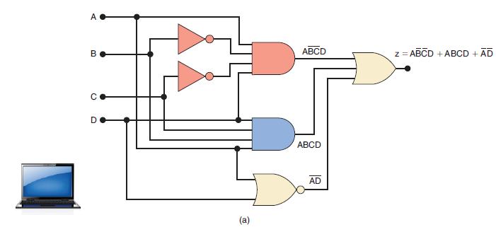
Refer to Figure 4-8(a), where an analog-to-digital converter is monitoring the dc voltage (VB) of a 12-V storage battery on an orbiting spaceship. The converter’s output is a four-bit binary number, ABCD, corresponding to the battery voltage in steps of 1 V, with A as the MSB. The converter’s
Simplify x = AB̅C + A̅BD + C̅D̅.
Design a logic circuit that has three inputs, A, B, and C, and whose output will be HIGH only when a majority of the inputs are HIGH.
Refer to Figure 4-9(a). In a simple copy machine, a stop signal, S, is to be generated to stop the machine operation and energize an indicator light whenever either of the following conditions exists: (1) there is no paper in the paper feeder tray; or (2) the two microswitches in the paper path are
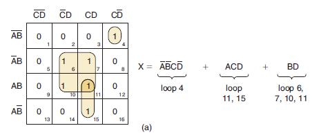
Figure 4-15(a) shows the K map for a four-variable problem. We will assume that Step 1 (construct a K map from the problem truth table) has been completed.The squares are numbered for convenience in identifying each loop. Use steps 2–7 of the simplification process to reduce the K map to an SOP
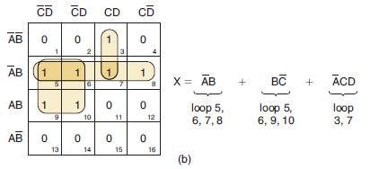
Consider the K map in Figure 4-15(b). Once again, we can assume that step 1 has already been performed. Simplify.Figure 4-15(b) AB AB AB AB CD CD 0 1 1 0 9 13 0 1 1 0 2 6 10 14 CD 1 0 0 11 15 CD 0 1 0 0 8 12 16 X = AB loop 5, 6,7,8 (b) + BC loop 5, 6, 9, 10 + ACD loop 3,7
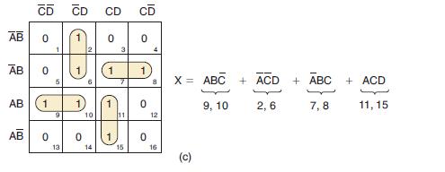
Consider the K map in Figure 4-15(c). Simplify.Figure 4-15(c) AB CD CD 0 AB 0 AB 1 AB 0 1 9 13 1 1 0 2 6 10 14 CD CD 204 0 0 1 11 15 0 0 8 12 16 X = ABC 7 (c) 9, 10 + ACD 2,6 + ABC 7,8 + ACD 11, 15
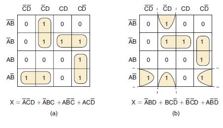
Consider the two K map loopings in Figure 4-16. Is one better than the other?Figure 4-16 AB AB CD CD CD AB 0 0 1 AB 000 1 00 UAD 1 1 1 1 ¹8 0 1 1 X = ACD + ABC + ABC + ACD (a) AB AB AB AB CD CD CD 0 0 0 1 0 1 0 1 0 0 CD 0 1 1 1 X = ABD + BCD + BCD +ABD (b)
Use a K map to simplify y = C(ABD + D) + ABC + D.
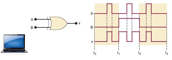
Determine the output waveform for the input waveforms given in Figure 4-22.Figure 4-22 A. I ве B A B to t₁ 1₂
When simplifying the expression for the output of a combinational logic circuit, you may encounter the XOR or XNOR operations as you are factoring. This will often lead to the use of XOR or XNOR gates in the implementation of the final circuit. To illustrate, simplify the circuit of Figure
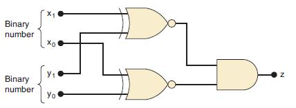
The notation x1x0 represents a two-bit binary number that can have any value (00, 01, 10, or 11); for example, when x1 = 1 and x0 = 0, the binary number is 10, and so on. Similarly, y1y0 represents another two-bit binary number. Design a logic circuit, using x1, x0, y1, and y0 inputs, whose output
Showing 1200 - 1300
of 1612
First
3
4
5
6
7
8
9
10
11
12
13
14
15
16
17
Step by Step Answers
![SUBDESIGN Figure 4-63 ( ) P, q, r S VARIABLE status [2..0] BEGIN END CASE; : INPUT; :OUTPUT; END; :NODE;](https://dsd5zvtm8ll6.cloudfront.net/images/question_images/1699/6/8/7/564654f2c8c0ec641699687563891.jpg)
![SUBDESIGN Figure 4-57 digital_value [3..0] ( Z BEGIN IF digital value [] > 6 THEN z = VCC; ELSE z = GND; END](https://dsd5zvtm8ll6.cloudfront.net/images/question_images/1699/6/8/7/041654f2a8109be01699687041803.jpg)
![SUBDESIGN Figure 4-57 digital_value [3..0] ( Z ) BEGIN IF digital_value [] > 6 THEN z = VCC; ELSE z = GND;](https://dsd5zvtm8ll6.cloudfront.net/images/question_images/1699/6/9/2/481654f3fc127b2b1699692481835.jpg)