New Semester
Started
Get
50% OFF
Study Help!
--h --m --s
Claim Now
Question Answers
Textbooks
Find textbooks, questions and answers
Oops, something went wrong!
Change your search query and then try again
S
Books
FREE
Study Help
Expert Questions
Accounting
General Management
Mathematics
Finance
Organizational Behaviour
Law
Physics
Operating System
Management Leadership
Sociology
Programming
Marketing
Database
Computer Network
Economics
Textbooks Solutions
Accounting
Managerial Accounting
Management Leadership
Cost Accounting
Statistics
Business Law
Corporate Finance
Finance
Economics
Auditing
Tutors
Online Tutors
Find a Tutor
Hire a Tutor
Become a Tutor
AI Tutor
AI Study Planner
NEW
Sell Books
Search
Search
Sign In
Register
study help
computer science
digital systems principles and application
Digital Systems Principles And Application 12th Edition Ronald Tocci, Neal Widmer, Gregory Moss - Solutions
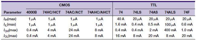
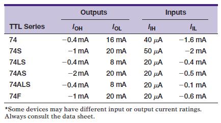
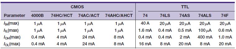
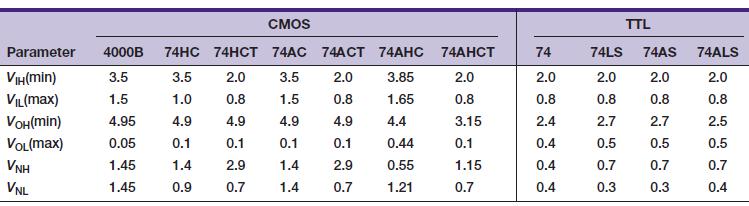
(a) Use Table 8-11 to determine how many 74AS inputs can typically be driven by a 4000B output.(b) Repeat part (a) for a 74HC output.Table 8-11 Parameter 4000B 1 μA 1 μA 0.4 mA 0.4 mA TIH(max) IL (max) JOH(max) TOL(max) CMOS 74HC/HCT 1 μA 1 μA 4 mA 4 mA 74AC/ACT 1 μA 1 μA 24 mA 24
(a) Which CMOS series can have its inputs driven directly from a TTL output?(b) What is the function of a level translator? When is it used?(c) Why is a buffer required between some CMOS outputs and TTL inputs?(d) True or false: Most CMOS outputs have trouble supplying the TTL HIGH-state input
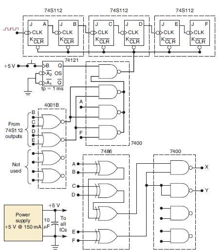
Figure 8-66 is a logic circuit that was poorly designed. It contains at least eight instances where the characteristics of the ICs have not been properly taken into account. Find as many of these as you can.Figure 8-66 nnn +5V J FCCLK CLR From 74S1 12 outputs Not used 74S112 A ▶B -A₂ OS LODA₁
Repeat Problem 8-42 with the following changes in the circuit:■ Each TTL IC is replaced with its 74LS equivalent.■ The 4001B is replaced with a 74HCT02.Data from Problem 8-42Figure 8-66 is a logic circuit that was poorly designed. It contains at least eight instances where the characteristics
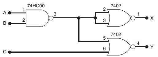
Use Table 8-11 to explain why the circuit of Figure 8-67 will not work as it is. How can the problem be corrected?Table 8-11Figure 8-67 Parameter 4000B 1 μA 1 μA 0.4 mA 0.4 mA TIH(max) IL (max) JOH(max) TOL(max) CMOS 74HC/HCT 1 μA 1 μA 4 mA 4 mA 74AC/ACT 1 μA 1 μA 24 mA 24 mA 74AHC/AHCT 1
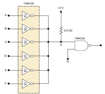
The circuit in Figure 8-68 uses a 74HC05 IC that contains six opendrain INVERTERs. The INVERTERs are connected in a wired- AND arrangement. The output of the NAND gate is always HIGH, regardless of the inputs A–H. Describe a procedure that uses a logic probe and pulser to isolate this
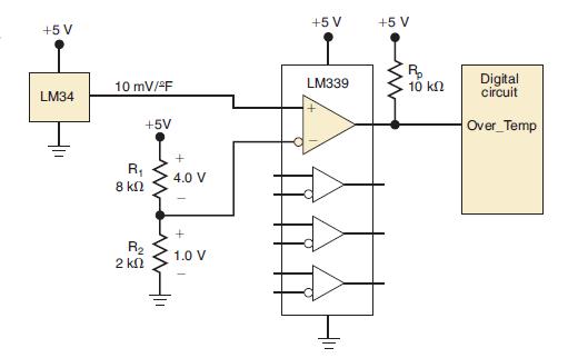
The over-temperature comparator circuit in Figure 8-49 is modified by replacing the LM34 temperature sensor with an LM35 that outputs 10 mV per degree Celsius. The alarm must still be activated (HIGH) when the temperature is over 100°F, which is equal to approximately 38ºC. Recalculate the values
The gas tank on your car has a fuel-level sending unit that works like a potentiometer. A float moves up and down with the gasoline level, changing the variable resistor setting and producing a voltage proportional to the gas level. A full tank produces 12 V, and an empty tank produces 0 V. Design
How does the TTL NOR circuit differ from the NAND circuit?
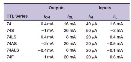
Refer to the data in Table 8-7 and determine how many 74AS20 NAND gates can be driven by the output of another 74AS20.Table 8-7 Outputs IOH -0.4 mA -1 MA -0.4 mA -2mA TTL Series 74 74S 74LS 74AS 74ALS 74F *Some devices may have different input or output current ratings. Always consult the data
What logic family combines the best features of CMOS and bipolar logic?
Which TTL series can drive the most device inputs of the same series?
Which low-voltage series can work only with other low-voltage series ICs?
Why do open-collector outputs need a pull-up resistor?
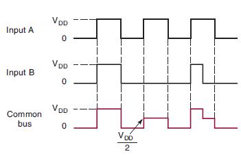
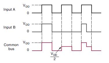
What conditions are necessary to transmit signal C onto the bus in Figure 8-37?Figure 8-37 Input A Input B Common bus VDD 0 VDD 0 VDD 0 V po 2
Which IC package can be plugged into sockets?
How many 7400 inputs can be driven from a 74HCT00 output?
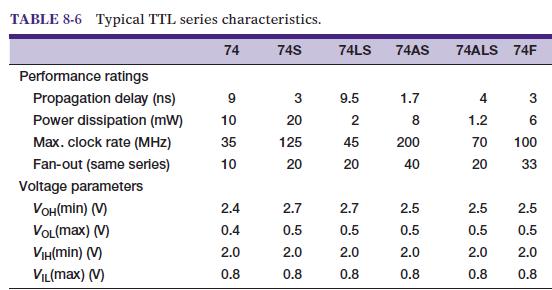
(a) From Table 8-6, determine the noise margins when a 74LS device is driving a 74ALS input.(b) Repeat part (a) for a 74ALS driving a 74LS.(c) What will be the overall noise margin of a logic circuit that uses 74LS and 74ALS circuits in combination?(d) A certain logic circuit has VIL(max) = 450 mV.
Which TTL transistor is the pull-down transistor in the NOR circuit?
What is power-supply decoupling? Why is it used?
What factors determine CMOS fan-out?
How many 74ALS00 NAND gate inputs can be driven by a 74ALS00 NAND gate output?
Which low-voltage series is fully electrically compatible with TTL?
What is the logic expression for the wired-AND connection of six 7406 outputs?
What is the IEEE/ANSI designation for tristate outputs?
Which package has leads bent under the IC?
(a) Define fan-out.(b) In which type of gates do tied-together inputs always count as a single input load in the LOW state?(c) Define “floating” inputs.(d) What causes current spikes in TTL? What undesirable effect can they produce? What can be done to reduce this effect?(e) When a TTL output
What precautions should be taken when handling CMOS ICs?
Why are open-collector outputs generally slower than totem-pole outputs?
Use Table 8-11 to find the fan-out for interfacing the first logic family to drive the second.(a) 74AS to 74AS(b) 74F to 74F(c) 74AHC to 74AS(d) 74HC to 74ALSTable 8-11 Parameter 4000B JIH(max) 1 μA TIL(max) 1 μA JOH(max) 0.4 mA TOL(max) 0.4 mA CMOS 74HC/HCT 1 μA 1 μA 4 mA 4 mA 74AC/ACT 1 μA 1
How do surface-mount packages differ from DIPs?
A 74ALS00 NAND gate output is driving three 74S gate inputs and one 7406 input. Using data from Table 8-7, determine if there is a loading problem.Table 8-7 Outputs IOH -0.4 mA -1 MA -0.4 mA -2mA TTL Series 74 74S 74LS 74AS 74ALS 74F *Some devices may have different input or output current
Which IC family (CMOS, TTL) is best suited for battery-powered applications?
What is the IEEE/ANSI symbol for open-collector outputs?
Will a standard TTL device work with an input level of 1.7 V?
True or false:(a) CMOS power drain increases with operating frequency.(b) Unused CMOS inputs can be left unconnected.(c) TTL is better suited than CMOS for operation in high-noise environments.(d) CMOS switching speed increases with operating frequency.(e) CMOS switching speed increases with supply
The 74ALS00 NAND gate output in Example 8-7 needs to be used to drive some 74ALS inputs in addition to the load inputs described in Example 8-7. How many additional 74ALS inputs could the output drive without being overloaded?Data from Example 8-7A 74ALS00 NAND gate output is driving three 74S gate
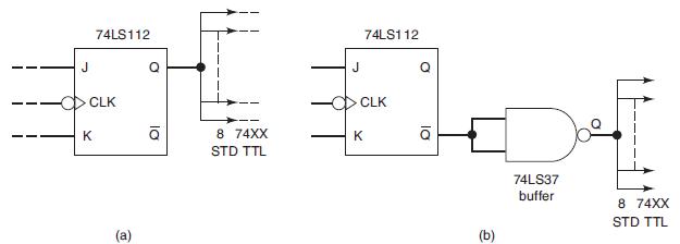
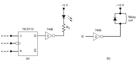
Figure 8-52(a) shows a 74LS112 J-K flip-flop whose output is required to drive a total of eight standard TTL inputs. Because this exceeds the fan-out of the 74LS112, a buffer of some type is needed. Figure 8-52(b) shows one possibility using one of the NAND gates from the 74LS37 quad NAND buffer,
Buffer gates are generally more expensive than ordinary gates, and sometimes there are unused ordinary gates available that can be used to solve a loading problem such as that in Figure 8-52(a). Show how 74LS00 NAND gates can be used to solve this problem.Figure 8-52 J 74LS112 K Q TE 8 74XX STD
The output of a 74AS04 inverter is providing the CLEAR signal to a parallel register made up of 74AS74A D flip-flops. What is the maximum number of FF C̅L̅R̅ inputs that this gate can drive?
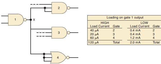
Determine the load that the X output is driving in Figure 8-16. Assume that each gate is a 74LS series device with IIH = 20 μA and IIL = 0.4 mA.Figure 8-16. X 2 3 Loading on gate 1 output HIGH Load Current 40 μA 20 μA 60 μA 1120 ΜΑ Gate 2 3 4 Total LOW Load Current 0.4 mA 0.4 mA 1.2 mA 2.0
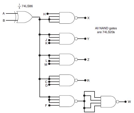
Refer to the logic diagram of Figure 8-53, where the 74LS86 exclusive-OR output is driving several 74LS20 inputs. Determine whether the fan-out of the 74LS86 is being exceeded, and explain. Repeat using all 74AS devices. Use Table 8-7.Figure 8-53Table 8-7 A B +74LS86 H M 00 X F Z R All NAND
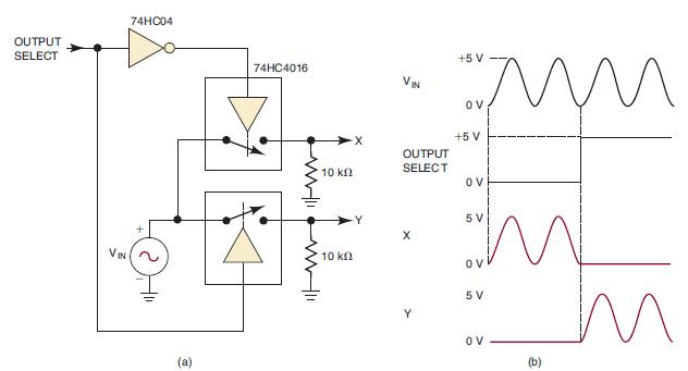
Describe the operation of the circuit in Figure 8-42.Figures 8-42 OUTPUT SELECT 74HC04 (a) 74HC4016 10 ΚΩ 10 k VIN OUTPUT SELECT X +5 V OV +5 V OV М 5 V 5 V OV (b) и
Determine an acceptable value for R if the OS is a 74LS TTL IC with an IIL input rating of 0.4 mA.
How long does it take for the output of a typical 74LS04 to change states in response to a positive-going transition at its input?
For the circuit of Figure 8-53, determine the longest time it will take for a change in the A input to be felt at output w. Use all worst-case conditions and maximum values of gate propagation delays. (Remember that NAND gates are inverting gates.) Repeat using all 74ALS devices.Figure 8-53
A 74HC output is driving three 7406 inputs. Is this a good design?
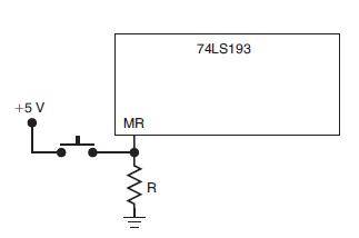
(a) Figure 8-54 shows a 74LS193 counter with its active-HIGH master reset input activated by a push-button switch. Resistor R is used to hold MR LOW while the switch is open. What is the maximum value that can be used for R?(b) Repeat part (a) for the 74ALS193.Figure 8-54 +5 V بما MR R 74LS193
A 4001B output is driving three 74LS inputs. Is this a well-designed circuit?
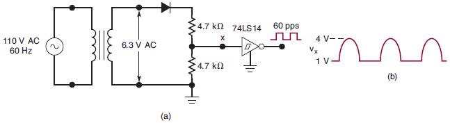
Figure 8-55(a) shows a circuit used to convert a 60-Hz sine wave to a 60-pps signal that can reliably trigger FFs and counters. This type of circuit might be used in a digital clock.(a) Explain the circuit operation.(b) A technician is testing this circuit and observes that the 74LS14 output stays
Suppose that an incubator must have an emergency alarm to warn if the temperature exceeds a dangerous level. The temperature-measuring device is an LM34 that puts out a voltage directly proportional to the temperature. The output voltage goes up 10 mV per degree F. The digital system alarm must
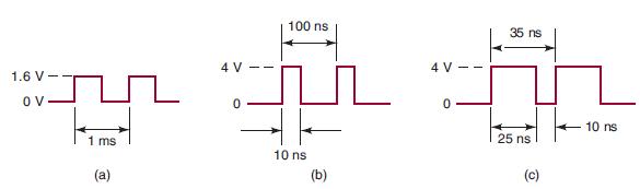
For each waveform in Figure 8-56, determine why it will not reliably trigger a 74LS112 flip-flop at its ClK input.Figure 8-56. 1.6 V- OV 1 ms (a) r 4 V- 0 100 ns 10 ns n (b) 4 V 0 35 ns 25 ns (c) 10 ns
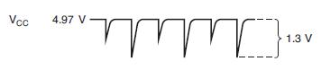
A technician breadboards a logic circuit for testing. As she tests the circuit’s operation, she finds that many of the FFs and counters are triggering erratically. Like any good technician, she checks the VCC line with a DC meter and reads 4.97 V, which is acceptable for TTL. She then checks all
Which type of MOSFET is turned on by placing (a) 5 V on the gate and 0 V on the source?(b) 0 V on the gate and 5 V on the source?
Which of the following are advantages that CMOS generally has over TTL?(a) Greater packing density(b) Higher speed(c) Greater fan-out(d) Lower output impedance(e) Simpler fabrication process(f) More suited for LSI(g) Lower PD (below 1 MHz)(h) Transistors as only circuit element(i) Lower input
Use the values from Table 8-9 to calculate the HIGH-state noise margin when a 74HC gate drives a standard 74LS input.Table 8-9 CMOS Parameter 4000B 74HC 74HCT 74AC 74ACT 74AHC 3.5 3.5 2.0 3.5 2.0 3.85 1.5 1.0
Which of the following operating conditions will probably result in the lowest average PD for a CMOS logic system? Explain.(a) VDD = 5 V, switching frequency fmax = 1 MHz(b) VDD = 5 V, fmax = 10 kHz(c) VDD = 10 V, fmax = 10 kHz
The output of each INVERTER on a 74LS04 IC is driving two 74HCT08 inputs. The input to each INVERTER is LOW over 99% of the time. What is the maximum power that the 74LS04 chip is dissipating?
What will cause latch-up in a CMOS IC? What might happen in this condition? What precautions should be taken to prevent latch-up?
Refer to the data sheet for the 74HC20 NAND gate IC. Use maximum values to calculate PD(avg) and tpd(avg). Compare with the values calculated in Problem 8-2 for TTL.Data from Problem 8-2Look up the IC data sheets, and use maximum values to determine PD(avg) and tpd(avg) for one gate on each of the
(a) Define wired-AND.(b) What is a pull-up resistor? Why is it used?(c) What types of TTL outputs can safely be tied together?(d) What is bus contention?
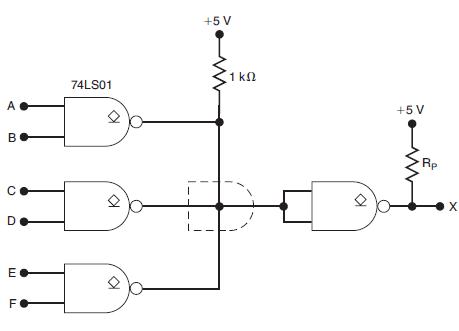
Determine the logic expression for output X in Figure 8-58.Figure 8-58 A B се D E FO 74LS01 +5 V 1 ΚΩ +5V Rp X
The 74LS09 TTL IC is a quad two-input AND with open-collector outputs. Show how 74LS09s can be used to implement the operation x = A · B · C · D · E · F · g · h · I · J · K · M.
Figure 8-59(a) shows a 7406 open-collector inverting buffer used to control the ON/OFF status of an LED to indicate the state of FF output Q. The LED’s nominal specification is VF = 2.4 V at IF = 20 mA, and IF(max) = 30 mA.(a) What voltage will appear at the 7406 output when Q = 0?(b) Choose an
Which of the following would be most likely to destroy a TTL totempole output while it is trying to switch from HIGH to LOW?(a) Tying the output to +5 V(b) Tying the output to ground(c) Applying an input of 7 V(d) Tying the output to another TTL totem-pole output
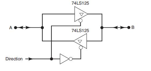
Figure 8-60 shows how two tristate buffers can be used to construct a bidirectional transceiver that allows digital data to be transmitted in either direction (A to B, or B to A). Describe the circuit operation for the two states of the DIRECTION input.Figure 8-60 A Direction 74LS125 74LS125 B
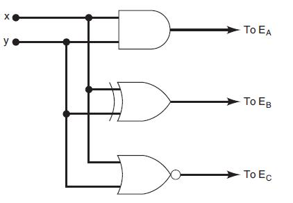
The circuit of Figure 8-61 is used to provide the enable inputs for the circuit of Figure 8-37.(a) Determine which of the data inputs (A, B, or C) will appear on the bus for each combination of inputs x and y.(b) Explain why the circuit will not work if the NOR is changed to an XNOR.Figure
What type of counter circuit from Chapter 7 could control the enables in Figure 8-37 so that only one buffer is on at any time, and the buffers are enabled sequentially?Figure 8-37 Input A Input B Common bus VDD 0 VDD 0 VDD 0 VDD 2
A Ping ultrasonic ranging module can measure distance based on the time it takes for sound to travel to an object and for the echo to return to the module. The user must provide a positive logic pulse to generate the burst of ultrasound (bang). Immediately after the bang, the module output goes
(a) How is resistance present in all transmission lines?(b) How is inductance present in all transmission lines?(c) How is capacitance present in all transmission lines?(d) The combined effects of the R, L, and C components of a transmission line is referred to as the line’s ______________?(e)
Assume that it takes 2 ns for the output of a full adder to settle after the inputs have changed. For a 16-bit adder, what is the longest amount of time (worst case) to add two numbers?
Add the following pairs of binary numbers.(a) 10110 + 00111(b) 011.101 + 010.010(c) 10001111 + 00000001
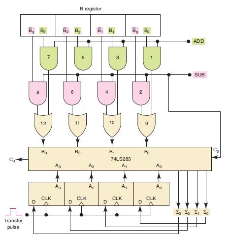
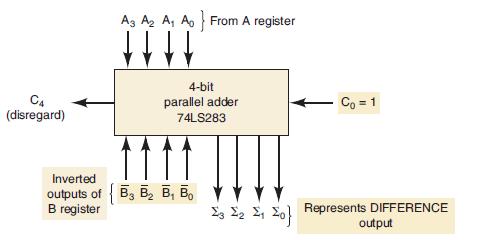
Why does C0 have to be a 1 in order to use the adder circuit in Figure 6-13 as a subtractor?Figure 6-13 C4 (disregard) A3 A₂ A₁ Ao From A register 4-bit parallel adder 74LS283 Inverted outputs of B3 B₂ B₁ B₂ B register Co = 1 23 22 2₁ 20 Represents DIFFERENCE output
How many 74HC283 chips are needed to add two 20-bit numbers?
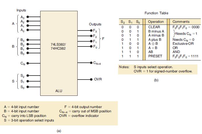
Apply the following inputs to the ALU of Figure 6-15, and determine the outputs: S2S1S0 = 001, A3A2A1A0 = 1110, B3B2B1B0 = 1001, CN = 1.Figure 6.15 A B S Inputs A3 B3 B₂ B₁ Bo CN S₁ So 74LS382/ 74HC382 A = 4-bit input number B = 4-bit input number CN = carry into LSB position S = 3-bit
Represent each of the following values as an eight-bit signed number in the 2’s-complement system.(a) +13 (b) –7 (c) –128
Assume the 2’s-complement system.True or false: Assume that the sum falls within the valid range for the number of bits. Whenever the sum of two signed binary numbers has a sign bit of 1, the magnitude of the sum is in 2’s-complement form.
Where can you find information about using a 74283 parallel adder macrofunction in your schematic design?
If [A] = 1001 and [B] = 0011, what is the value of(a) [A] · [B]? (b) [A] + [B]? (Note that · means AND; + means OR.)
Perform the subtraction on the following pairs of signed numbers using the 2’s-complement system. Express the results as signed binary numbers and as decimal values.(a) 01001 – 11010 (b) 10010 – 10011
Multiply the unsigned numbers 0111 and 1110.
How can you tell when a correction is needed in BCD addition?
Modify the AHDL code in Figure 6-23 to create a 4-bit parallel adder.Figure 6-23 1 SUBDESIGN fig6_23 495SWNT 2 ( 3 a [7..0] b[7..0] s [8..0] 6 ) 7 VARIABLE aa [8..0] bb [8..0] BEGIN aa [8..0] = bb [8..0] = s [8..0] END; 098 10 11 12 13 14 M = : INPUT; :INPUT; :OUTPUT; :NODE; :NODE; (GND, a
Add 67F + 2A4.
Name the three blocks of an arithmetic logic unit.
What keyword is used to assign a symbolic name to a fixed number?
How many inputs does a full adder have? How many outputs?
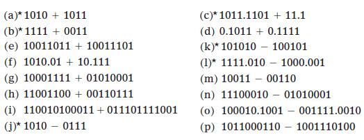
Add or subtract the following in binary. Check your results by converting the numbers and doing the calculations in decimal. (a)* 1010 1011 (b)* 1111 0011 (e) 10011011 + 10011101 (f) 1010.0110.111 (g) 10001111 + 01010001 (h) 11001100+ 00110111 (i) 110010100011+011101111001 (j)* 1010 0111 (c)*
Represent each of the following signed decimal numbers as a signed binary number in the 2’s-complement system. Use a total of five bits, including the sign bit.(a) +13 (b) –9 (c) +3 (d) –2 (e) –8
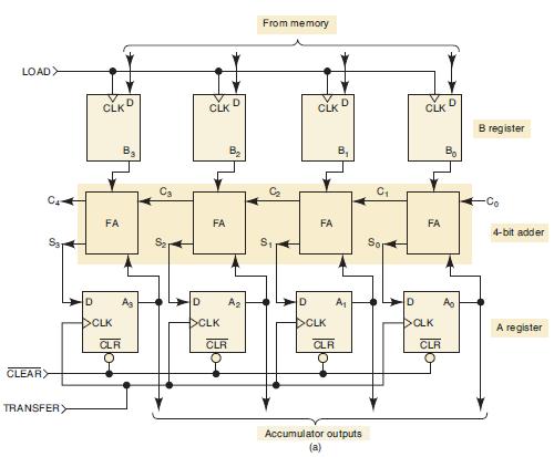
Suppose that four different four-bit numbers are to be taken from memory and added by the circuit of Figure 6-10. How many CLEAR pulses will be needed? How many TRANSFER pulses? How many LOAD pulses?Figure 6.10 LOAD CLEAR S31 TRANSFER> CLKD FA D >CLK CLR B₂ As 8 CO D CLK
What is the highest frequency that the accumulator register can be clocked?
Subtract the following pairs of binary numbers:(a) 101101 - 010010(b) 10001011 - 00110101(c) 10101.1101 - 01110.0110
Assume that [A] = 0011 and [B] = 0010 in Figure 6-14. If ADD = 1 and SUB = 0, determine the logic levels at the OR gate outputs.Figure 6-14 Transfer pulse BB₂ 0 12 B3 CLK Ag { B₂ B₂ 6 D B register 11 B₂ 01 CLK A₂ A₂ B₁ B₁ D 10 3₂ B₁ 74LS283 A₁ A₁ CLK B₁
If a 74HC283 has a maximum propagation delay of 30 ns from C0 to C4, what will be the total propagation delay of a 32-bit adder constructed from 74HC283s?
Change the select code to 011 and CN to 0, and repeat review question 1.Data from question 1Apply the following inputs to the ALU of Figure 6-15, and determine the outputs: S2S1S0 = 001, A3A2A1A0 = 1110, B3B2B1B0 = 1001, CN = 1.Figure 6.15
Each of the following is a signed binary number in the 2’s-complement system. Determine the decimal equivalent for each.(a) 100011 (b) 1000000 (c) 01111110
Assume the 2’s-complement system. Add the following pairs of signed numbers. Express the sum as a signed binary number and as a decimal number.(a) 100111 + 111011 (b) 100111 + 011001
What is a macrofunction?
If A[7..0] = 1010 1100, what is the value of (a) A[7..4]? (b) A[5..2]?
How can arithmetic overflow be detected when signed numbers are being added? Subtracted?
Showing 600 - 700
of 1612
1
2
3
4
5
6
7
8
9
10
11
12
13
14
15
Last
Step by Step Answers
![1 SUBDESIGN fig6_23 495SWNT 2 ( 3 a [7..0] b[7..0] s [8..0] 6 ) 7 VARIABLE aa [8..0] bb [8..0] BEGIN aa](https://dsd5zvtm8ll6.cloudfront.net/images/question_images/1699/8/6/0/9906551d1feac35a1699860989919.jpg)